

Page 1
The MC13155 is a complete wideband FM detector designed for satellite
TV and other wideband data and analog FM applications. This device may
be cascaded for higher IF gain and extended Receive Signal Strength
Indicator (RSSI) range.
• 12 MHz Video/Baseband Demodulator
• Ideal for Wideband Data and Analog FM Systems
• Limiter Output for Cascade Operation
• Low Drain Current: 7.0 mA
• Low Supply Voltage: 3.0 to 6.0 V
• Operates to 300 MHz
Order this document by MC13155/D
WIDEBAND FM IF
SEMICONDUCTOR
TECHNICAL DATA
MAXIMUM RATINGS
Rating Pin Symbol Value Unit
Power Supply Voltage 11, 14 VEE (max) 6.5 Vdc
Input Voltage 1, 16 V
Junction Temperature – T
Storage Temperature Range – T
NOTE: Devices should not be operated at or outside these values. The “Recommended
Operating Conditions” provide for actual device operation.
in
J
stg
1.0 Vrms
+150 °C
– 65 to +150 °C
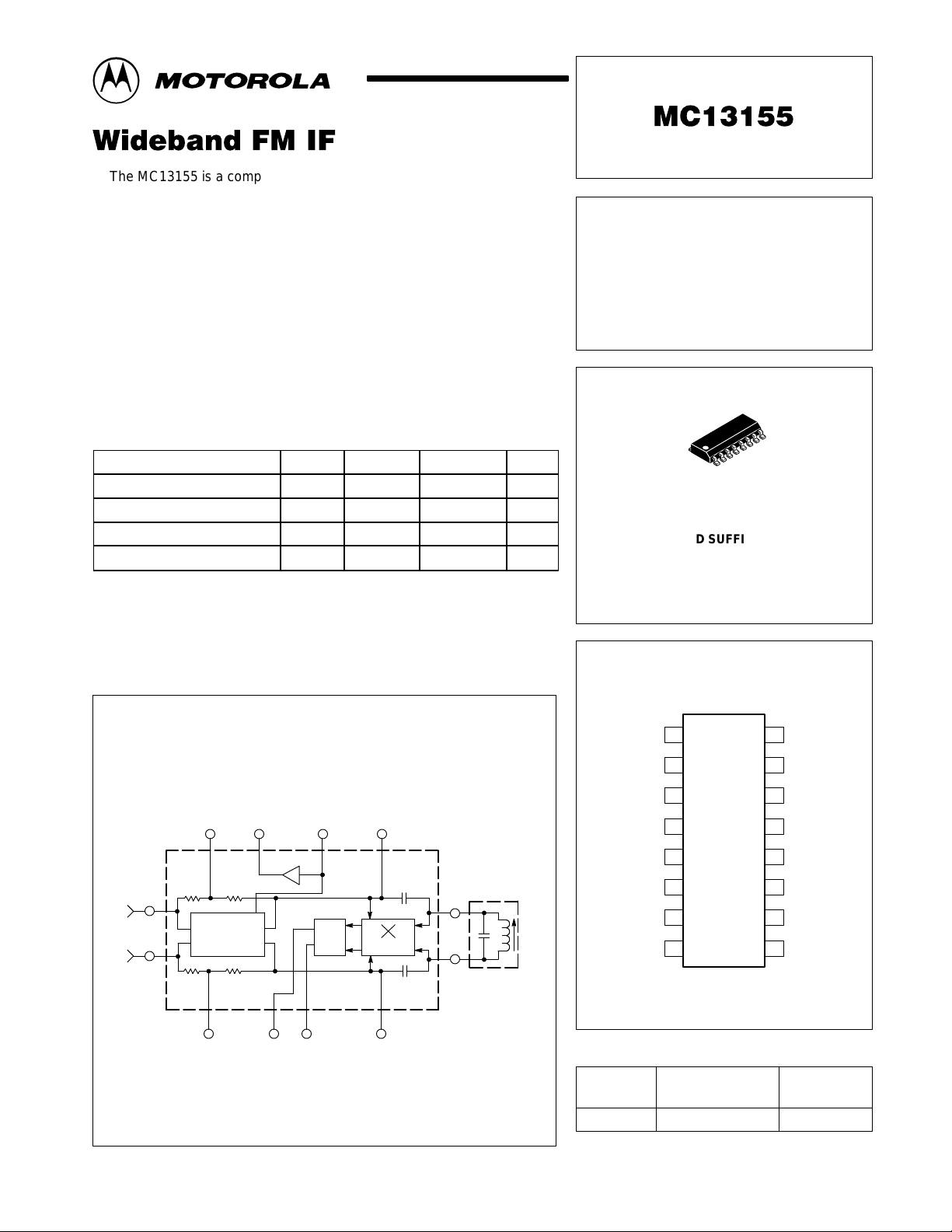
Figure 1. Representative Block Diagram
Buffered
Input
Input
16
RSSI
Decouple
1
Output
15
Three Stage
Amplifier
RSSI
Output
Limiter
Output
101213
9
Detector
8
Quad
Coil
Input
Decouple
VCC1
Output
Output
VCC2
Limiter Out
Quad Coil
16
1
D SUFFIX
PLASTIC PACKAGE
CASE 751B
(SO–16)
PIN CONNECTIONS
1
2
3
4
5
6
7
8
(Top View)
16
15
14
13
12
11
10
9
Input
Decouple
VEE1
RSSI Buffer
RSSI
VEE2
Limiter Out
Quad Coil
7542
Decouple
NOTE: This device requires careful layout and decoupling to ensure stable operation.
Balanced
Outputs
Limiter
Output
MOTOROLA ANALOG IC DEVICE DATA
ORDERING INFORMATION
Operating
Device
MC13155D TA = – 40 to +85°C SO–16
Motorola, Inc. 1996 Rev 1
Temperature Range
Package
1
Page 2
MC13155
RECOMMENDED OPERATING CONDITIONS
Rating Pin Symbol Value Unit
Power Supply Voltage (TA= 25°C) 11, 14 V
–40°C ≤ TA ≤ 85°C 3, 6 V
Maximum Input Frequency 1, 16 f
Ambient Temperature Range – T
EE
CC
in
J
– 3.0 to – 6.0 Vdc
Grounded
300 MHz
– 40 to + 85 °C
DC ELECTRICAL CHARACTERISTICS (T
Characteristic
Drain Current 11 I
(VEE = – 5.0 Vdc) 14 I
(VEE = – 5.0 Vdc) 14 I
Drain Current Total (see Figure 3) 11, 14 I
(VEE = – 5.0 Vdc) 5.0 7.5 10.5
(VEE = – 6.0 Vdc) 5.0 7.5 10.5
(VEE = – 3.0 Vdc) 4.7 6.6 9.5
AC ELECTRICAL CHARACTERISTICS (T
Characteristic
Input for – 3 dB Limiting Sensitivity 1, 16 – 1.0 2.0 mVrms
Differential Detector Output Voltage (Vin = 10 mVrms) 4, 5 mV
(f
= ± 3.0 MHz) (VEE = – 6.0 Vdc) 470 590 700
dev
Detector DC Offset Voltage 4, 5 –250 – 250 mVdc
RSSI Slope 13 1.4 2.1 2.8 µA/dB
RSSI Dynamic Range 13 31 35 39 dB
RSSI Output 12 µA
(Vin = 100 µVrms) – 2.1 –
(Vin = 1.0 mVrms) – 2.4 –
(Vin = 10 mVrms) 16 24 36
(Vin = 100 mVrms) – 65 –
(Vin = 500 mVrms) – 75 –
RSSI Buffer Maximum Output Current (Vin = 10 mVrms) 13 – 2.3 – mAdc
Differential Limiter Output mVrms
(Vin = 1.0 mVrms) 7, 10 100 140 –
(Vin = 10 mVrms) – 180 –
Demodulator Video 3.0 dB Bandwidth 4, 5 – 12 – MHz
Input Impedance (Figure 14) 1, 16
@ 70 MHz Rp (VEE = – 5.0 Vdc) – 450 – Ω
@ 70 MHz Cp (C2=C15 = 100 p) – 4.8 – pF
Differential IF Power Gain 1, 7, 10, 16 – 46 – dB
NOTE: Positive currents are out of the pins of the device.
(VEE = – 5.0 Vdc) 450 570 680
(VEE = – 3.0 Vdc) 380 500 620
= 25°C, no input signal.)
A
Pin Symbol Min Typ Max Unit
11
14
14
Total
= 25°C, fIF = 70 MHz, VEE = – 5.0 Vdc Figure 2, unless otherwise noted.)
A
2.0 2.8 4.0 mA
3.0 4.3 6.0
3.0 4.3 6.0
5.0 7.1 10 mA
Pin Min Typ Max Unit
p–p
2
MOTOROLA ANALOG IC DEVICE DATA
Page 3
MC13155
CIRCUIT DESCRIPTION
The MC13155 consists of a wideband three–stage limiting
amplifier, a wideband quadrature detector which may be
operated up to 200 MHz, and a received signal strength
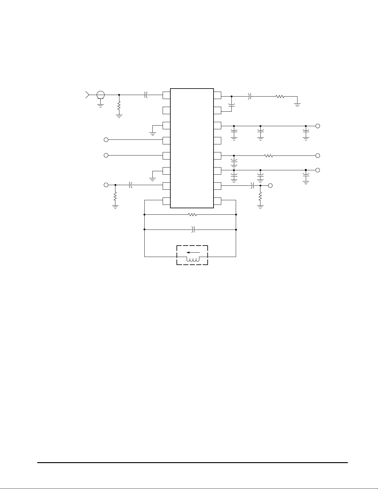
Figure 2. T est Circuit
1.0n
V
in
Video
Output
Limiter 1
Output
49.9
1.0n
330
1
2
3
4
5
6
7
8
IN1
DEC1
VCC1
DETO1
DETO2
VCC2
LIMO1
indicator (RSSI) circuit which provides a current output
linearly proportional to the IF input signal level for
approximately 35 dB range of input level.
IN2
DEC2
VEE1
RSSI
Buffer
RSSI
VEE2
LIMO2
QUAD2QUAD1
16
15
14
13
12
11
10
1.0n
10n
1.0n
1.0n
1.0n
1.0n
9
100n
1.0k
100n
330
27
Limiter 2
Output
10
10
V
µ
µ
EE
+
V
EE
V
EE
+
APPLICATIONS INFORMATION
Evaluation PC Board
The evaluation PCB shown in Figures 19 and 20 is very
versatile and is designed to cascade two ICs. The center
section of the board provides an area for attaching all surface
mount components to the circuit side and radial leaded
components to the component ground side of the PCB (see
Figures 17 and 18). Additionally, the peripheral area
surrounding the RF core provides pads to add supporting
and interface circuitry as a particular application dictates.
This evaluation board will be discussed and referenced in
this section.
Limiting Amplifier
Differential input and output ports interfacing the three
stage limiting amplifier provide a differential power gain of
typically 46 dB and useable frequency range of 300 MHz.
The IF gain flatness may be controlled by decoupling of the
internal feedback network at Pins 2 and 15.
499
20p
L1
260n
L1 – Coilcraft part number 146–09J08S
Scattering parameter (S–parameter) characterization of
the IF as a two port linear amplifier is useful to implement
maximum stable power gain, input matching, and stability
over a desired bandpass response and to ensure stable
operation outside the bandpass as well. The MC13155 is
unconditionally stable over most of its useful operating
frequency range; however, it can be made unconditionally
stable over its entire operating range with the proper
decoupling of Pins 2 and 15. Relatively small decoupling
capacitors of about 100 pF have a significant effect on the
wideband response and stability. This is shown in the
scattering parameter tables where S–parameters are shown
for various values of C2 and C15 and at VEE of – 3.0 and
– 5.0 Vdc.
MOTOROLA ANALOG IC DEVICE DATA
3
Page 4

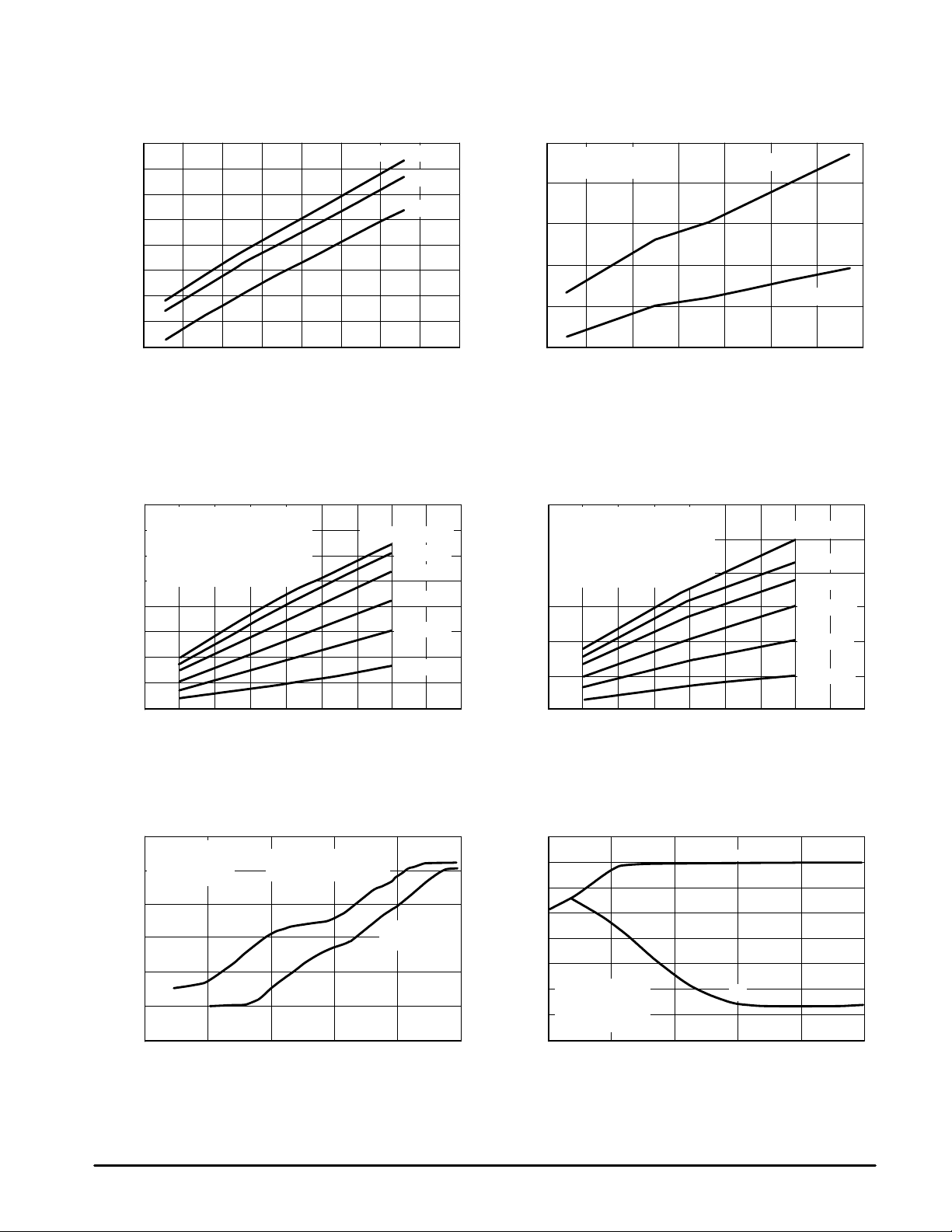
TYPICAL PERFORMANCE AT TEMPERATURE
Figure 3. Drain Current versus Supply Voltage
10
TA = 25°C
8.0
6.0
4.0
, DRAIN CURRENT (mAdc)
Total
2.0
and I
14
I
0.0
0.0
1.0 2.0 3.0 4.0 5.0 6.0 7.0 8.0 100 1000
I
= I14 + I
Total
VEE, SUPPLY VOLTAGE (–Vdc)
11
I
14
MC13155
(See Figure 2. T est Circuit)
Figure 4. RSSI Output versus Frequency and
100
80
µ
60
40
RSSI OUTPUT ( A)
12
I ,
20
0
10
Input Signal Level
VEE = – 5.0Vdc
0 dBm
–10 dBm
– 20 dBm
– 30 dBm
– 40 dBm
f, FREQUENCY (MHz)
Figure 5. T otal Drain Current versus Ambient
T emperature and Supply Voltage
8.5
8.0
7.5
7.0
6.5
TOTAL DRAIN CURRENT (mAdc)
6.0
14
5.5
and I ,
11
5.0
I
–50 – 30 –10 10 30 50 70 90 110 –50 – 30 –10 10 30 50 70 90 110
TA, AMBIENT TEMPERATURE (°C)
VEE = – 6.0 Vdc
– 3.0 Vdc
– 5.0 Vdc
Figure 7. RSSI Output versus Ambient
T emperature and Supply Voltage
µ
RSSI OUTPUT ( A)
12
I ,
25.0
24.5
24.0
23.5
23.0
22.5
22.0
VEE = – 6.0 Vdc
VEE = – 5.0 Vdc
VEE = – 3.0 Vdc
Figure 6. Detector Drain Current and Limiter
Drain Current versus Ambient Temperature
5.59.0
f = 70 MHz
5.0
VEE = – 5.0 Vdc
4.5
4.0
3.5
DRAIN CURRENT (mAdc)
3.0
11
2.5
14
I and I ,
2.0
TA, AMBIENT TEMPERATURE (
Figure 8. RSSI Output versus Input Signal
V oltage (Vin at Temperature)
100
TA = + 85°C
µ
RSSI OUTPUT ( A)
12
I ,
80
60
40
20
I
14
I
11
°
C)
+25°C
–40°C
21.5
4
0
– 30 –10 10 30 50 70 90 110 1.0 10 100 1000
–50
0.1
Vin, INPUT VOLTAGE (mVrms)TA, AMBIENT TEMPERATURE (°C)
MOTOROLA ANALOG IC DEVICE DATA
Page 5
MC13155
Figure 9. Differential Detector Output
V oltage versus Ambient Temperature
and Supply V oltage
750 220
700
650
600
pp
550
500
(Pins 4, 5), (mV )
450
400
DIFFERENTIAL DETECTOR OUTPUT VOLTAGE
350
–50 – 30 –10 10 30 50 70 90 110
VEE = – 6.0 Vdc
– 5.0 Vdc
– 3.0 Vdc
Figure 11A. Differential Detector Output Voltage
versus Q of Quadrature LC Tank
)
1600
Vin = – 30 dBm
pp
VEE = – 5.0 Vdc
1400
fc = 70 MHz
f
1200
1000
800
600
400
200
DIFFERENTIAL DETECTOR OUTPUT (mV
= 1.0 MHz
mod
(Figure 16 no external capacitors
between Pins 7, 8 and 9, 10)
0
1.5
2.5 3.5 4.5 5.5
2.0 3.0 4.0 5.0 6.0 1.5 2.5 3.5 4.5 5.52.0 3.0 4.0 5.0 6.0
Q OF QUADRATURE LC TANK
f
= ±6.0 MHz
dev
±
5.0 MHz
±
4.0 MHz
±
3.0 MHz
±
2.0 MHz
±
1.0 MHz
Figure 10. Differential Limiter Output Voltage
versus Ambient T emperature
(Vin = 1 and 10 mVrms)
f = 70 MHz
VEE = – 5.0 Vdc
200
180
160
(Pins 7, 10), (mVrms)
140
DIFFERENTIAL LIMITER OUTPUT VOLTAGE
120
–50 – 30 –10 10 30 50 70 90
TA, AMBIENT TEMPERATURE (°C)TA, AMBIENT TEMPERATURE (°C)
Vin = 10 mVrms
Vin = 1.0 mVrms
Figure 11B. Differential Detector Output Voltage
versus Q of Quadrature LC Tank
)
2400
Vin = – 30 dBm
pp
2000
1600
1200
800
400
0
DIFFERENTIAL DETECTOR OUTPUT (mV
VEE = – 5.0 Vdc
fc = 70 MHz
f
= 1.0 MHz
mod
(Figure 16 no external capacitors
between Pins 7, 8 and 9, 10)
Q OF QUADRATURE LC TANK
f
= ±6.0 MHz
dev
±
5.0 MHz
±
4.0 MHz
±
3.0 MHz
±
2.0 MHz
±
1.0 MHz
Figure 11.
Figure 12. RSSI Output V oltage versus IF Input
0
VEE = – 5.0 Vdc
fc = 70 MHz
–1.0
(See Figure 16)
–2.0
–3.0
–4.0
–5.0
RSSI OUTPUT VOLTAGE, (Vdc)
–80 –60 –40 –20 0 20
Capacitively coupled
interstage: no attenuation
15 dB Interstage
Attenuator
IF INPUT, (dBm)
MOTOROLA ANALOG IC DEVICE DATA
Figure 13. – S+N, N versus IF Input
10
0
–10
–20
–30
S+N, N (dB)
–40
fc = 70 MHz
–50
f
= 1.0 MHz
mod
±
5.0 MHz
f
=
dev
–60
VEE = – 5.0 Vdc
–70
–90 – 70 – 50 – 30 –10 10
IF INPUT (dBm)
S+N
N
5
Page 6

MC13155
In the S–parameters measurements, the IF is treated as a
two–port linear class A amplifier. The IF amplifier is
measured with a single–ended input and output configuration
in which the Pins 16 and 7 are terminated in the series
combination of a 47 Ω resistor and a 10 nF capacitor to V
CC
ground (see Figure 14. S–Parameter Test Circuit).
The S–parameters are in polar form as the magnitude
(MAG) and angle (ANG). Also listed in the tables are the
calculated values for the stability factor (K) and the Maximum
Figure 14. S–Parameter T est Circuit
IF
Input
SMA
1.0n
C2
1
2
3
4
5
IN1
DEC1
VCC1
DETO1
DETO2
Available Gain (MAG). These terms are related in the
following equations:
K = (1– IS11 I2 – I S22 I2 + I ∆ I2 ) / ( 2 I S12 S21 I )
where: I ∆ I = I S11 S22 – S12 S21 I.
MAG = 10 log I S21 I / I S12 I + 10 log I K – ( K2 – 1)
1/2
I
where: K > 1. The necessary and sufficient conditions for
unconditional stability are given as K > 1:
B1 = 1 + I S11 I2 – I S22 I2 – I ∆ I2 > 0
IN2
DEC2
VEE1
RSSI
Buffer
RSSI
1.0n
16
C15
15
14
13
12
47
V
EE
100n1.0n
10
µ
+
47
1.0n
6
7
8
VCC2
LIMO1
VEE2
LIMO2
QUAD2QUAD1
11
10
SMA
1.0n
9
IF
Output
6
MOTOROLA ANALOG IC DEVICE DATA
Page 7

MC13155
S–Parameters (V
Frequency Input S1 1 Forward S21 Rev S12 Output S22 K MAG
MHz MAG ANG MAG ANG MAG ANG MAG ANG MAG dB
1.0 0.94 –13 8.2 143 0.001 7.0 0.87 –22 2.2 32
2.0 0.78 –23 23.5 109 0.001 –40 0.64 –31 4.2 33.5
5.0 0.48 1.0 39.2 51 0.001 –97 0.34 –17 8.7 33.7
7.0 0.59 15 40.3 34 0.001 –41 0.33 –13 10.6 34.6
10 0.75 17 40.9 19 0.001 –82 0.41 –1.0 5.7 36.7
20 0.95 7.0 42.9 – 6.0 0.001 –42 0.45 0 1.05 46.4
50 0.98 –10 42.2 –48 0.001 – 9.0 0.52 – 3.0 0.29 –
70 0.95 –16 39.8 –68 0.001 112 0.54 –16 1.05 46.4
100 0.93 –23 44.2 –93 0.001 80 0.53 –22 0.76 –
150 0.91 –34 39.5 –139 0.001 106 0.50 –34 0.94 –
200 0.87 –47 34.9 –179 0.002 77 0.42 –44 0.97 –
500 0.89 –103 11.1 –58 0.022 57 0.40 –117 0.75 –
700 0.61 –156 3.5 –164 0.03 0 0.52 179 2.6 13.7
900 0.56 162 1.2 92 0.048 –44 0.47 112 4.7 4.5
1000 0.54 131 0.8 42 0.072 –48 0.44 76 5.1 0.4
S–Parameters (V
Frequency Input S1 1 Forward S21 Rev S12 Output S22 K MAG
MHz MAG ANG MAG ANG MAG ANG MAG ANG MAG dB
1.0 0.98 –15 11.7 174 0.001 –14 0.84 –27 1.2 37.4
2.0 0.50 – 2.0 39.2 85.5 0.001 –108 0.62 –35 6.0 35.5
5.0 0.87 8.0 39.9 19 0.001 100 0.47 – 9.0 4.2 39.2
7.0 0.90 5.0 40.4 9.0 0.001 –40 0.45 – 8.0 3.1 40.3
10 0.92 3.0 41 1.0 0.001 –40 0.44 – 5.0 2.4 41.8
20 0.92 – 2.0 42.4 –14 0.001 –87 0.49 – 6.0 2.4 41.9
50 0.91 – 8.0 41.2 –45 0.001 85 0.50 – 5.0 2.3 42
70 0.91 –11 39.1 –63 0.001 76 0.52 – 4.0 2.2 41.6
100 0.91 –15 43.4 –84 0.001 85 0.50 –11 1.3 43.6
150 0.90 –22 38.2 –126 0.001 96 0.43 –22 1.4 41.8
200 0.86 –33 35.5 –160 0.002 78 0.43 –21 1.3 39.4
500 0.80 –66 8.3 – 9.0 0.012 75 0.57 –63 1.7 23.5
700 0.62 –96 2.9 –95 0.013 50 0.49 –111 6.3 12.5
900 0.56 –120 1.0 –171 0.020 53 0.44 –150 13.3 2.8
1000 0.54 –136 0.69 154 0.034 65 0.44 –179 12.5 – 0.8
= – 5.0 Vdc, TA = 25°C, C2 and C15 = 0 pF)
EE
= – 5.0 Vdc, TA = 25°C, C2 and C15 = 100 pF)
EE
MOTOROLA ANALOG IC DEVICE DATA
7
Page 8

MC13155
S–Parameters (V
Frequency Input S1 1 Forward S21 Rev S12 Output S22 K MAG
MHz MAG ANG MAG ANG MAG ANG MAG ANG MAG dB
1.0 0.74 4.0 53.6 110 0.001 101 0.97 –35 0.58 –
2.0 0.90 3.0 70.8 55 0.001 60 0.68 –34 1.4 45.6
5.0 0.91 0 87.1 21 0.001 –121 0.33 –60 1.1 49
7.0 0.91 0 90.3 11 0.001 –18 0.25 –67 1.2 48.4
10 0.91 – 2.0 92.4 2.0 0.001 33 0.14 –67 1.5 47.5
20 0.91 – 4.0 95.5 –16 0.001 63 0.12 –15 1.3 48.2
50 0.90 – 8.0 89.7 –50 0.001 –43 0.24 26 1.8 46.5
70 0.90 –10 82.6 –70 0.001 92 0.33 21 1.4 47.4
100 0.91 –14 77.12 –93 0.001 23 0.42 –1.0 1.05 49
150 0.94 –20 62.0 –122 0.001 96 0.42 –22 0.54 –
200 0.95 –33 56.9 –148 0.003 146 0.33 –62 0.75 –
500 0.82 –63 12.3 –12 0.007 79 0.44 –67 1.8 26.9
700 0.66 –98 3.8 –107 0.014 84 0.40 –115 4.8 14.6
900 0.56 –122 1.3 177 0.028 78 0.39 –166 8.0 4.7
1000 0.54 –139 0.87 141 0.048 76 0.41 165 7.4 0.96
S–Parameters (V
Frequency Input S1 1 Forward S21 Rev S12 Output S22 K MAG
MHz MAG ANG MAG ANG MAG ANG MAG ANG MAG dB
1.0 0.89 –14 9.3 136 0.001 2.0 0.84 –27 3.2 30.7
2.0 0.76 –22 24.2 105 0.001 –90 0.67 –37 3.5 34.3
5.0 0.52 5.0 35.7 46 0.001 –32 0.40 –13 10.6 33.3
7.0 0.59 12 38.1 34 0.001 –41 0.40 –10 9.1 34.6
10 0.78 15 37.2 16 0.001 –92 0.40 –1.0 5.7 36.3
20 0.95 5.0 38.2 – 9.0 0.001 47 0.51 – 4.0 0.94 –
50 0.96 –11 39.1 –50 0.001 –103 0.48 – 6.0 1.4 43.7
70 0.93 –17 36.8 –71 0.001 –76 0.52 –13 2.2 41.4
100 0.91 –25 34.7 –99 0.001 –152 0.51 –19 3.0 39.0
150 0.86 –37 33.8 –143 0.001 53 0.49 –34 1.7 39.1
200 0.81 –49 27.8 86 0.003 76 0.55 –56 2.4 35.1
500 0.70 –93 6.2 –41 0.015 93 0.40 –110 2.4 19.5
700 0.62 –144 1.9 –133 0.049 56 0.40 –150 3.0 8.25
900 0.39 –176 0.72 125 0.1 1 –18 0.25 163 5.1 –1.9
1000 0.44 166 0.49 80 0.10 –52 0.33 127 7.5 – 4.8
= – 5.0 Vdc, TA = 25°C, C2 and C15 = 680 pF)
EE
= – 3.0 Vdc, TA = 25°C, C2 and C15 = 0 pF)
EE
8
MOTOROLA ANALOG IC DEVICE DATA
Page 9

MC13155
S–Parameters (V
Frequency Input S1 1 Forward S21 Rev S12 Output S22 K MAG
MHz MAG ANG MAG ANG MAG ANG MAG ANG MAG dB
1.0 0.97 –15 11.7 171 0.001 – 4.0 0.84 –27 1.4 36.8
2.0 0.53 2.0 37.1 80 0.001 –91 0.57 –31 6.0 34.8
5.0 0.88 7.0 37.7 18 0.001 – 9.0 0.48 – 7.0 3.4 39.7
7.0 0.90 5.0 37.7 8.0 0.001 –11 0.49 – 7.0 2.3 41
10 0.92 2.0 38.3 1.0 0.001 –59 0.51 – 9.0 2.0 41.8
20 0.92 – 2.0 39.6 –15 0.001 29 0.48 – 3.0 1.9 42.5
50 0.91 – 8.0 38.5 –46 0.001 –21 0.51 – 7.0 2.3 41.4
70 0.91 –11 36.1 –64 0.001 49 0.50 – 8.0 2.3 40.8
100 0.91 –15 39.6 –85 0.001 114 0.52 –13 1.7 37.8
150 0.89 –22 34.4 –128 0.001 120 0.48 –23 1.6 40.1
200 0.86 –33 32 –163 0.002 86 0.40 –26 1.7 37.8
500 0.78 –64 7.6 –12 0.013 94 0.46 –71 1.9 22.1
700 0.64 –98 2.3 –102 0.027 58 0.42 –109 4.1 10.1
900 0.54 –122 0.78 179 0.040 38.6 0.35 –147 10.0 – 0.14
1000 0.53 –136 0.47 144 0.043 23 0.38 –171 15.4 – 4.52
S–Parameters (V
Frequency Input S1 1 Forward S21 Rev S12 Output S22 K MAG
MHz MAG ANG MAG ANG MAG ANG MAG ANG MAG dB
1.0 0.81 3.0 37 101 0.001 –19 0.90 –32 1.1 43.5
2.0 0.90 2.0 47.8 52.7 0.001 –82 0.66 –39 0.72 –
5.0 0.91 0 58.9 20 0.001 104 0.37 –56 2.3 44
7.0 0.90 –1 60.3 11 0.001 –76 0.26 –55 2.04 44
10 0.91 – 2.0 61.8 3.0 0.001 105 0.18 –52 2.2 43.9
20 0.91 – 4.0 63.8 –15 0.001 59 0.11 –13 2.0 44.1
50 0.90 – 8.0 60.0 –48 0.001 96 0.22 33 2.3 43.7
70 0.90 –11 56.5 –67 0.001 113 0.29 15 2.3 43.2
100 0.91 –14 52.7 –91 0.001 177 0.36 5.0 2.0 43
150 0.93 –21 44.5 –126 0.001 155 0.35 –17 1.8 42.7
200 0.90 –43 41.2 –162 0.003 144 0.17 –31 1.6 34.1
500 0.79 –65 7.3 –13 0.008 80 0.44 –75 3.0 22
700 0.65 –97 2.3 –107 0.016 86 0.38 –124 7.1 10.2
900 0.56 –122 0.80 174 0.031 73 0.38 –174 12 0.37
1000 0.55 –139 0.52 137 0.50 71 0.41 157 11.3 – 3.4
= – 3.0 Vdc, TA = 25°C, C2 and C15 = 100 pF)
EE
= – 3.0 Vdc, TA = 25°C, C2 and C15 = 680 pF)
EE
MOTOROLA ANALOG IC DEVICE DATA
9
Page 10

MC13155
DC Biasing Considerations
The DC biasing scheme utilizes two VCC connections
(Pins 3 and 6) and two VEE connections (Pins 14 and 11).
VEE1 (Pin 14) is connected internally to the IF and RSSI
circuits’ negative supply bus while VEE2 (Pin 1 1) is connected
internally to the quadrature detector’s negative bus. Under
positive ground operation, this unique configuration offers the
ability to bias the RSSI and IF separately from the quadrature
detector. When two ICs are cascaded as shown in the 70
MHz application circuit and provided by the PCB (see
Figures 17 and 18), the first MC13155 is used without biasing
its quadrature detector, thereby saving approximately 3.0
mA. A total current of 7.0 mA is used to fully bias each IC,
thus the total current in the application circuit is
approximately 1 1 mA. Both VCC pins are biased by the same
supply. VCC1 (Pin 3) is connected internally to the positive
bus of the first half of the IF limiting amplifier, while VCC2 is
internally connected to the positive bus of the RSSI, the
quadrature detector circuit, and the second half of the IF
limiting amplifier (see Figure 15). This distribution of the V
enhances the stability of the IC.
RSSI Circuitry
The RSSI circuitry provides typically 35 dB of linear
dynamic range and its output voltage swing is adjusted by
CC
selection of the resistor from Pin 12 to VEE. The RSSI slope
is typically 2.1 µA/dB ; thus, for a dynamic range of 35 dB, the
current output is approximately 74 µA. A 47 k resistor will
yield an RSSI output voltage swing of 3.5 Vdc. The RSSI
buffer output at Pin 13 is an emitter–follower and needs an
external emitter resistor of 10 k to VEE.
In a cascaded configuration (see circuit application in
Figure 16), only one of the RSSI Buffer outputs (Pin 13) is
used; the RSSI outputs (Pin 12 of each IC) are tied together
and the one closest to the VEE supply trace is decoupled to
VCC ground. The two pins are connected to VEE through a 47
k resistor. This resistor sources a RSSI current which is
proportional to the signal level at the IF input; typically,
1.0 mVrms (– 47 dBm) is required to place the MC13155 into
limiting. The measured RSSI output voltage response of the
application circuit is shown in Figure 12. Since the RSSI
current output is dependent upon the input signal level at the
IF input, a careful accounting of filter losses, matching and
other losses and gains must be made in the entire receiver
system. In the block diagram of the application circuit shown
below, an accounting of the signal levels at points throughout
the system shows how the RSSI response in Figure 12 is
justified.
Block Diagram of 70 MHz Video Receiver Application Circuit
Input – 45 dBm – 70 dBm – 72 dBm – 32 dBm – 47 dBm Minimum Input to Acquire
Level: 1.26 mVrms 71
IF
Input
Saw
Filter
– 25 dB
(Insertion Loss)
µ
Vrms 57 µVrms 57 µVrms 1.0 mVrms Limiting in MC13155
16
1:4
Transformer
2.0 dB
(Insertion Loss)
1
Cascading Stages
The limiting IF output is pinned–out differentially,
cascading is easily achieved by AC coupling stage to stage.
In the evaluation PCB, AC coupling is shown, however,
interstage filtering may be desirable in some applications. In
which case, the S–parameters provide a means to implement
a low loss interstage match and better receiver sensitivity .
Where a linear response of the RSSI output is desired
when cascading the ICs, it is necessary to provide at least
10 dB of interstage loss. Figure 12 shows the RSSI response
with and without interstage loss. A 15 dB resistive attenuator
is an inexpensive way to linearize the RSSI response. This
has its drawbacks since it is a wideband noise source that is
dependent upon the source and load impedance and the
amount of attenuation that it provides. A better, although
more costly, solution would be a bandpass filter designed to
the desired center frequency and bandpass response while
carefully selecting the insertion loss. A network topology
10
MC13155
7
40 dB Gain
(Attenuator)
16
MC13155
1
40 dB Gain–15 dB
shown below may be used to provide a bandpass response
with the desired insertion loss.
Network Topology
1.0n
10
0.22
µ
7
1.0n
16
1
10
MOTOROLA ANALOG IC DEVICE DATA
Page 11

MC13155
Quadrature Detector
The quadrature detector is coupled to the IF with internal
2.0 pF capacitors between Pins 7 and 8 and Pins 9 and 10.
For wideband data applications, such as FM video and
satellite receivers, the drive to the detector can be increased
with additional external capacitors between these pins, thus,
the recovered video signal level output is increased for a
given bandwidth (see Figure 1 1A and Figure 11B).
The wideband performance of the detector is controlled by
the loaded Q of the LC tank circuit. The following equation
defines the components which set the detector circuit’s
bandwidth:
Q = RT/X
where: RT is the equivalent shunt resistance across the LC
T ank and XL is the reactance of the quadrature inductor at the
IF frequency (XL = 2πfL).
The inductor and capacitor are chosen to form a resonant
LC T ank with the PCB and parasitic device capacitance at the
desired IF center frequency as predicted by:
fc = (2π √(LCp))
where: L is the parallel tank inductor and Cp is the equivalent
parallel capacitance of the parallel resonant tank circuit.
The following is a design example for a wideband detector
at 70 MHz and a loaded Q of 5. The loaded Q of the
quadrature detector is chosen somewhat less than the Q of
the IF bandpass. For an IF frequency of 70 MHz and an
IF bandpass of 10.9 MHz, the IF bandpass Q is
approximately 6.4.
Example:
Let the external Cext = 20 pF. (The minimum value here
should be greater than 15 pF making it greater than the
internal device and PCB parasitic capacitance, Cint ≈
3.0 pF).
Cp = Cint + Cext = 23 pF
Rewrite Equation 2 and solve for L:
L = (0.159)2 /(Cp fc2)
L = 198 nH, thus, a standard value is chosen.
L = 0.22 µH (tunable shielded inductor).
L
–1
(1)
(2)
The value of the total damping resistor to obtain the
required loaded Q of 5 can be calculated by rearranging
Equation 1:
RT = Q(2πfL)
RT = 5 (2π)(70)(0.22) = 483.8 Ω.
The internal resistance, Rint between the quadrature tank
Pins 8 and 9 is approximately 3200 Ω and is considered in
determining the external resistance, Rext which is calculated
from:
Rext = ((RT)(Rint))/ (Rint – RT)
Rext = 570, thus, choose the standard value.
Rext = 560 Ω.
SAW Filter
In wideband video data applications, the IF occupied
bandwidth may be several MHz wide. A good rule of thumb is
to choose the IF frequency about 10 or more times greater
than the IF occupied bandwidth. The IF bandpass filter is a
SAW filter in video data applications where a very selective
response is needed (i.e., very sharp bandpass response).
The evaluation PCB is laid out to accommodate two SAW
filter package types: 1) A five–leaded plastic SIP package.
Recommended part numbers are Siemens X6950M which
operates at 70 MHz; 10.4 MHz 3 dB passband, X6951M
(X252.8) which operates at 70 MHz; 9.2 MHz 3 dB passband;
and X6958M which operates at 70 MHz, 6.3 MHz 3 dB
passband, and 2) A four–leaded TO–39 metal can package.
Typical insertion loss in a wide bandpass SA W filter is 25 dB.
The above SAW filters require source and load
impedances of 50 Ω to assure stable operation. On the PC
board layout, space is provided to add a matching network,
such as a 1:4 surface mount transformer between the SAW
filter output and the input to the MC13155. A 1:4 transformer,
made by Coilcraft and Mini Circuits, provides a suitable
interface (see Figures 16, 17 and 18). In the circuit and
layout, the SAW filter and the MC13155 are differentially
configured with interconnect traces which are equal in length
and symmetrical. This balanced feed enhances RF stability,
phase linearity , and noise performance.
MOTOROLA ANALOG IC DEVICE DATA
11
Page 12

2
CC
V
LIM Out
MC13155
Det
5
1.0p
Out
Figure 15.
4
2V
1114116
EE
V
Quad Coil
1.6k 1.6k
2.0p 2.0p
LIM Out
Figure 15. Simplified Internal Circuit Schematic
1
CC
V
8.0k
8.0k
1
EE
Bias Bias
12
Decouple
15 2 13 12 3 10 9 8 7 6
RSSIRSSI
Buffer
InputInput
10p
1.0k 1.0k
MOTOROLA ANALOG IC DEVICE DATA
Page 13

If Input
1
2
3
SAW Filter is Siemens
Part Number X6950M
SAW Filter
MC13155
Figure 16. 70 MHz Video Receiver Application Circuit
1:4
5
4
220
1.0n1.0n
100p
1
2
3
4
5
6
7
IN1
DEC1
VCC1
DETO1
DETO2
VCC2
LIMO1
MC13155
DEC2
Buffer
LIMO2
IN2
VEE1
RSSI
RSSI
VEE2
16
15
14
13
12
11
10
100p
10n
Output
10n
1.0n
RSSI
47k
10k
100n
Detector
Output
100n
100n
33p
33p
1.0k
1.0k
820
100p
2.0p
8
1
2
3
4
5
6
7
8
QUAD1
MC13155
IN1
DEC1
VCC1
DETO1
DETO2
VCC2
LIMO1
QUAD1
820
820
560
QUAD2
IN2
DEC2
VEE1
RSSI
Buffer
RSSI
VEE2
LIMO2
QUAD2
16
15
14
13
12
11
10
9
+
820
1.0n1.0n
100p
10n
10
10n
2.0p
9
µ
+
10
µ
VEE2
VEE1
MOTOROLA ANALOG IC DEVICE DATA
20p
0.22
L
L– Coilcraft part number 146–08J08S
µ
13
Page 14

MC13155
Figure 17. Component Placement (Circuit Side)
Figure 18. Component Placement (Ground Side)
14
MOTOROLA ANALOG IC DEVICE DATA
Page 15

MC13155
Figure 19. Circuit Side View
4.0
″
4.0
″
Figure 20. Ground Side View
MOTOROLA ANALOG IC DEVICE DATA
15
Page 16

SEATING
PLANE
1
G
–T
–
D
0.25 (0.010) T B A
16 PL
M
–A
–
S S
MC13155
OUTLINE DIMENSIONS
D SUFFIX
PLASTIC PACKAGE
CASE 751B
(SO–16)
NOTES:
1. DIMENSIONING AND TOLERANCING PER ANSI
Y14.5M, 1982.
2. CONTROLLING DIMENSION: MILLIMETER.
3. DIMENSION A AND B DO NOT INCLUDE MOLD
916
P
8 PL
0.25 (0.010)
–B
–
8
M M
B
X 45°
R
C
K
M
F
J
PROTRUSION.
4. MAXIMUM MOLD PROTRUSION 0.15 (0.006)
PER SIDE.
5. 751B–03 IS OBSOLETE, NEW STANDARD
751B–04.
MILLIMETERS INCHES
MIN MINMAX MAX
DIM
A
9.80
B
3.80
C
1.35
D
0.35
F
0.40
1.27 BSC 0.050 BSC
G
J
0.19
K
0.10
M
°
0
P
5.80
R
0.25
10.00
4.00
1.75
0.49
1.25
0.25
0.25
7
6.20
0.50
0.386
0.393
0.150
0.157
0.054
0.068
0.014
0.019
0.016
0.049
0.008
0.009
0.004
0.009
°
°
0
0.229
0.010
7
0.244
0.019
°
Motorola reserves the right to make changes without further notice to any products herein. Motorola makes no warranty, representation or guarantee regarding
the suitability of its products for any particular purpose, nor does Motorola assume any liability arising out of the application or use of any product or circuit, and
specifically disclaims any and all liability, including without limitation consequential or incidental damages. “T ypical” parameters which may be provided in Motorola
data sheets and/or specifications can and do vary in different applications and actual performance may vary over time. All operating parameters, including “Typicals”
must be validated for each customer application by customer’s technical experts. Motorola does not convey any license under its patent rights nor the rights of
others. Motorola products are not designed, intended, or authorized for use as components in systems intended for surgical implant into the body, or other
applications intended to support or sustain life, or for any other application in which the failure of the Motorola product could create a situation where personal injury
or death may occur. Should Buyer purchase or use Motorola products for any such unintended or unauthorized application, Buyer shall indemnify and hold Motorola
and its officers, employees, subsidiaries, affiliates, and distributors harmless against all claims, costs, damages, and expenses, and reasonable attorney fees
arising out of, directly or indirectly, any claim of personal injury or death associated with such unintended or unauthorized use, even if such claim alleges that
Motorola was negligent regarding the design or manufacture of the part. Motorola and are registered trademarks of Motorola, Inc. Motorola, Inc. is an Equal
Opportunity/Affirmative Action Employer.
Mfax is a trademark of Motorola, Inc.
How to reach us:
USA/EUROPE/Locations Not Listed: Motorola Literature Distribution; JAP AN: Nippon Motorola Ltd.: SPD, Strategic Planning Office, 4–32–1,
P.O. Box 5405, Denver, Colorado 80217. 303–675–2140 or 1–800–441–2447 Nishi–Gotanda, Shinagawa–ku, Tokyo 141, Japan. 81–3–5487–8488
Mfax: RMFAX0@email.sps.mot.com – TOUCHTONE 602–244–6609 ASIA/PACIFIC: Motorola Semiconductors H.K. Ltd.; 8B Tai Ping Industrial Park,
– US & Canada ONLY 1–800–774–1848 51 Ting Kok Road, T a i Po, N.T., Hong Kong. 852–26629298
INTERNET: http://motorola.com/sps
16
◊
MOTOROLA ANALOG IC DEVICE DATA
MC13155/D
 Loading...