

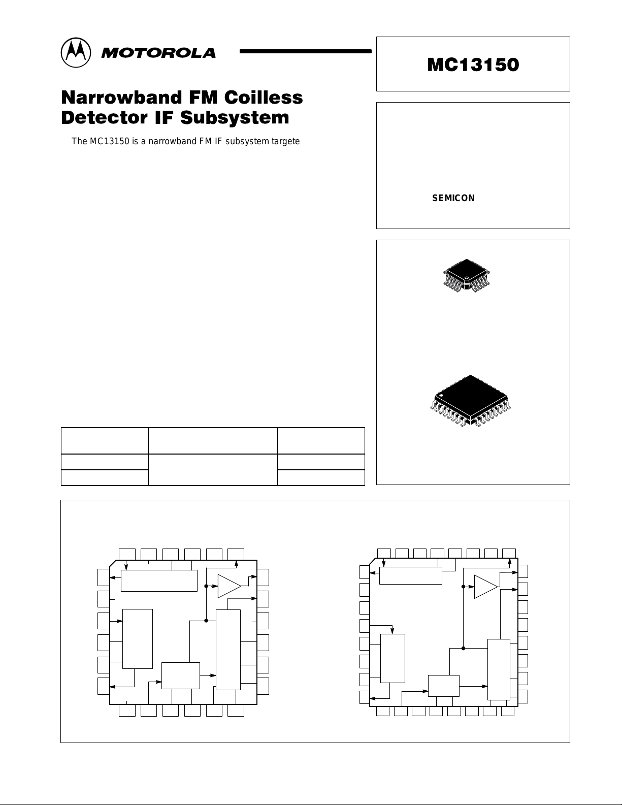
Page 1
T
85°C
Order this document by MC13150/D
The MC13150 is a narrowband FM IF subsystem targeted at cellular and
other analog applications. Excellent high frequency performance is
achieved, with low cost, through use of Motorola’s MOSAIC 1.5 RF bipolar
process. The MC13150 has an onboard Colpitts VCO for Crystal controlled
second LO in dual conversion receivers. The mixer is a double balanced
configuration with excellent third order intercept. It is useful to beyond
200 MHz. The IF amplifier is split to accommodate two low cost cascaded
filters. RSSI output is derived by summing the output of both IF sections. The
quadrature detector is a unique design eliminating the conventional tunable
quadrature coil.
Applications for the MC13150 include cellular, CT–1 900 MHz cordless
telephone, data links and other radio systems utilizing narrowband FM
modulation.
• Linear Coilless Detector
• Adjustable Demodulator Bandwidth
• 2.5 to 6.0 Vdc Operation
• Low Drain Current: <2.0 mA
• Typical Sensitivity of 2.0 µV for 12 dB SINAD
• IIP3, Input Third Order Intercept Point of 0 dBm
• RSSI Range of Greater Than 100 dB
• Internal 1.4 kΩ Terminations for 455 kHz Filters
• Split IF for Improved Filtering and Extended RSSI Range
ORDERING INFORMATION
Operating
Device
MC13150FT A
MC13150FTB
Temperature Range
–
°
= –40 ° to +
A
°
Package
LQFP–24
LQFP–32
NARROWBAND FM COILLESS
DETECTOR IF SUBSYSTEM
FOR CELLULAR AND
ANALOG APPLICATIONS
SEMICONDUCTOR
TECHNICAL DATA
24 1
FTA SUFFIX
PLASTIC PACKAGE
CASE 977
(LQFP–24)
32
1
FTB SUFFIX
PLASTIC PACKAGE
CASE 873
(LQFP–32)
LQFP–24 LQFP–32
PIN CONNECTIONS
Mix
V
out
CC1
IF
IF
IF
IF
out
d1
d2
in
EE1
V
Mix
24 23 22 21 20 19
1
2
3
in
4
5
6
Mixer
IF
789101112
in
CC2
LIM
V
LOeLO
Limiter
LIMd1LIM
d2
b
Enable
RSSI
Detector
AdjFAdj
BW
18
17
16
15
14
13
RSSI
DET
V
EE2
DET
AFT
AFT
b
out
Gain
Filt
out
Mix
Out
V
CC1
VCC (N/C)
IF
in
IF
d1
VCC (N/C)
IF
d2
IF
out
MOTOROLA ANALOG IC DEVICE DATA
in
Mix
32 31 28 27 26 2530 29
1
2
3
4
5
IF
6
7
8
910 1314151611 12
CC2
V
Motorola, Inc. 1997 Rev 2
EE1
V
Mixer
in
LIM
V
V
CC
CC
(N/C)
(N/C)
LOeLO
Limiter
LIMd1LIM
d2
b
CC
V
Enable
V
CC
(N/C)
(N/C)
Detector
AdjFAdj
BW
RSSI
24
23
22
21
20
19
18
17
RSSI
DET
VEE (N/C)
V
DET
VEE (N/C)
AFT
AFT
b
out
EE2
Gain
Filt
out
1
Page 2
MC13150
Á
Á
Á
Á
Á
Á
Á
Á
ÁÁÁÁ
Á
Á
Á
Á
Á
Á
ÁÁÁÁ
Á
Á
Á
Á
Á
ÁÁÁÁ
Á
Á
Á
Á
Á
ÁÁÁÁ
Á
Á
Á
Á
Á
ÁÁÁÁ
Á
Á
Á
Á
Á
Á
Á
Á
Á
Á
Á
Á
Á
Á
Á
Á
Á
Á
Á
Á
Á
Á
Á
Á
Á
Á
Á
Á
Á
Á
Á
Á
Á
Á
Á
Á
Á
Á
Á
Á
Á
Á
Á
Á
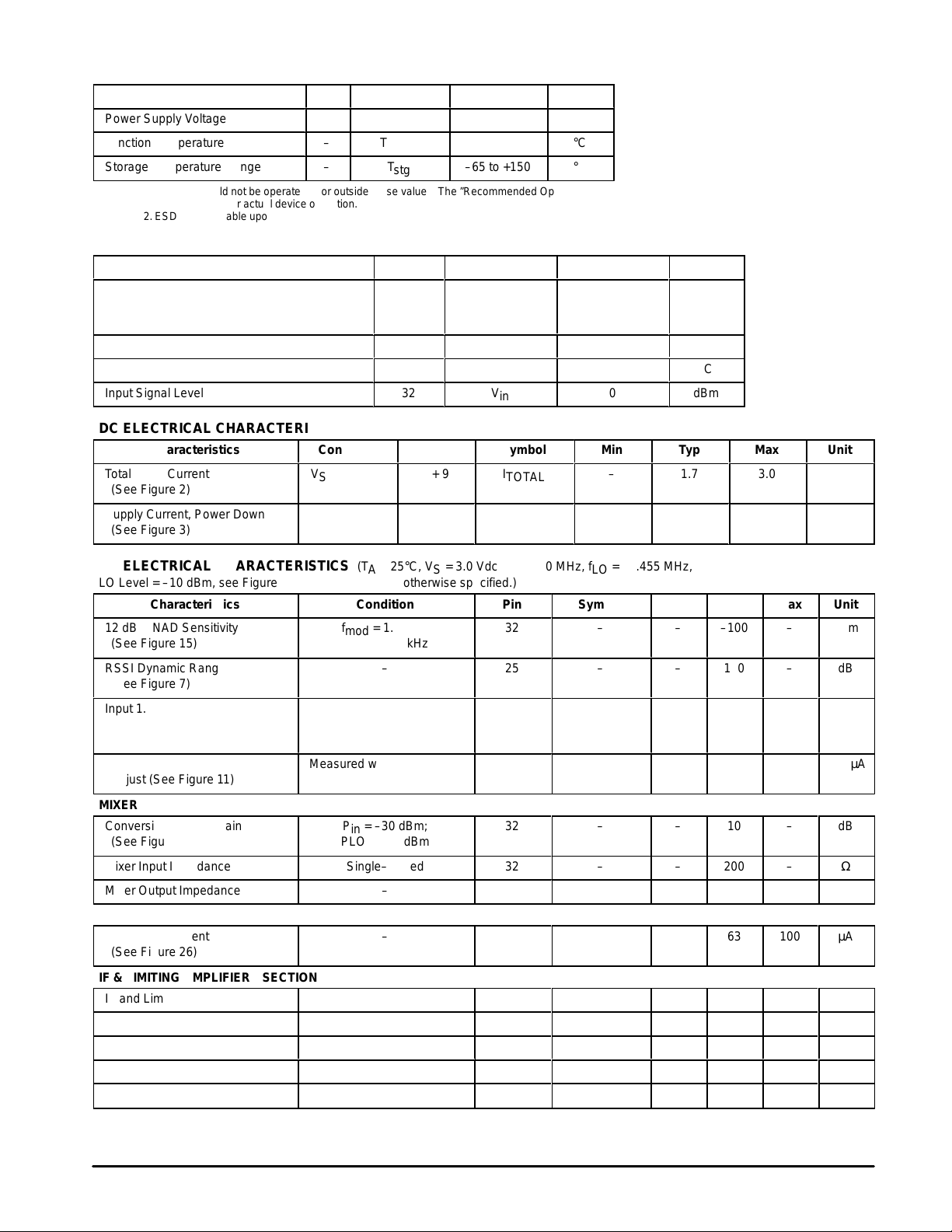
MAXIMUM RATINGS
Rating Pin Symbol Value Unit
Power Supply Voltage
Junction Temperature
Storage Temperature Range
NOTE: 1. Devices should not be operated at or outside these values. The ”Recommended Operating
Limits” provide for actual device operation.
2.ESD data available upon request.
RECOMMENDED OPERATING CONDITIONS
Rating Pin Symbol Value Unit
Power Supply Voltage TA = 25°C
БББББББББББ
(See Figure 22)
БББББББББББ
Input Frequency
БББББББББББ
Ambient Temperature Range
БББББББББББ
Input Signal Level
БББББББББББ
–40°C ≤ TA ≤ 85°C
2, 9
–
–
VCC(max)
T
Jmax
T
stg
2, 9
21, 31
ÁÁ
ÁÁ
32
ÁÁ
–
ÁÁ
32
ÁÁ
6.5
+150
–65 to +150
V
CC
V
ÁÁÁÁ
EE
ÁÁÁÁ
f
in
ÁÁÁÁ
T
A
ÁÁÁÁ
V
in
ÁÁÁÁ
Vdc
°C
°C
2.5 to 6.0
0
ÁÁÁÁ
ÁÁÁÁ
10 to 500
ÁÁÁÁ
–40 to +85
ÁÁÁÁ
0
ÁÁÁÁ
Vdc
ÁÁÁ
ÁÁÁ
MHz
ÁÁÁ
°C
ÁÁÁ
dBm
ÁÁÁ
DC ELECTRICAL CHARACTERISTICS (T
Characteristics
Total Drain Current
(See Figure 2)
ББББББББ
Supply Current, Power Down
Condition Pin Symbol Min Typ Max Unit
VS = 3.0 Vdc
ÁÁÁ
–
= 25°C, V
A
ÁÁ
CC1
2 + 9
2 + 9
= V
CC2
ÁÁÁÁ
(See Figure 3)
AC ELECTRICAL CHARACTERISTICS (T
= 25°C, VS = 3.0 Vdc, fRF = 50 MHz, fLO = 50.455 MHz,
A
LO Level = –10 dBm, see Figure 1 Test Circuit*, unless otherwise specified.)
Characteristics
12 dB SINAD Sensitivity
ББББББББ
(See Figure 15)
RSSI Dynamic Range
(See Figure 7)
ББББББББ
Input 1.0 dB Compression Point
Input 3rd Order Intercept Point
ББББББББ
(See Figure 18)
Coilless Detector Bandwidth
Adjust (See Figure 11)
ББББББББ
Condition Pin Symbol Min Typ Max Unit
f
= 1.0 kHz;
mod
ББББББ
f
= ±5.0 kHz
dev
ÁÁÁ
–
ББББББ
ÁÁÁ
–
ББББББ
–
ÁÁÁ
Measured with No IF Filters
ББББББ
ÁÁÁ
MIXER
Conversion Voltage Gain
(See Figure 5)
Mixer Input Impedance
Mixer Output Impedance
Pin = –30 dBm;
PLO = –10 dBm
Single–Ended
–
LOCAL OSCILLATOR
LO Emitter Current
ББББББББ
(See Figure 26)
ББББББ
–
ÁÁÁ
IF & LIMITING AMPLIFIERS SECTION
IF and Limiter RSSI Slope
IF Gain
IF Input & Output Impedance
Limiter Input Impedance
Limiter Gain
* Figure 1 Test Circuit uses positive (VCC) Ground.
Figure 7
Figure 8
–
–
–
= 3.0 Vdc, No Input Signal.)
I
TOTAL
–
32
25
–
–
–
32
32
1
29
25
4, 8
4, 8
10
–
–
ÁÁÁ
–
–
ÁÁÁ
–
ÁÁÁ
1.0 dB C. Pt.
IIP3
ÁÁÁ
∆BW adj
ÁÁÁ
–
–
–
–
ÁÁÁ
–
–
–
–
–
1.7
ÁÁ
40
–
Á
–
Á
–
–
Á
–
Á
–
–
–
30
Á
–
–
–
–
–
–100
Á
100
Á
–11
–1.0
Á
26
Á
10
200
1.5
63
Á
0.4
42
1.5
1.5
96
3.0
ÁÁ
–
ÁÁ
ÁÁ
ÁÁ
ÁÁ
ÁÁ
–
–
–
–
–
–
–
–
100
–
–
–
–
–
mA
ÁÁ
nA
dBm
Á
dB
Á
dBm
Á
kHz/µA
Á
dB
Ω
kΩ
µA
Á
µA/dB
dB
kΩ
kΩ
dB
2
MOTOROLA ANALOG IC DEVICE DATA
Page 3
MC13150
AC ELECTRICAL CHARACTERISTICS (continued) (T
LO Level = –10 dBm, see Figure 1 Test Circuit*, unless otherwise specified.)
Characteristics UnitMaxTypMinSymbolPinCondition
DETECTOR
Frequency Adjust Current Figure 9,
Frequency Adjust Voltage Figure 10,
Bandwidth Adjust Voltage Figure 12,
Detector DC Output Voltage
(See Figure 25)
Recovered Audio Voltage f
* Figure 1 Test Circuit uses positive (VCC) Ground.
fIF = 455 kHz
fIF = 455 kHz
I15 = 1.0 µA
– 23 – – 1.36 – Vdc
= ±3.0 kHz 23 – 85 122 175 mVrms
dev
= 25°C, VS = 3.0 Vdc, fRF = 50 MHz, fLO = 50.455 MHz,
A
Figure 1. T est Circuit
LO Input
Local
Oscillator
Limiter
Mixer
In
IF
In
49.9
IF Amp
Out
Mixer
Out
220 n
220 n
10
1:4
Z Xformer
220 n
1.5 k
220 n
220 n
220 n
1.5 k
µ
+
V
EE1
220 n
100 n
31 30 29 28 27 26 25
32
V
EE1
1
2
3
4
5
6
7
8
Mixer
V
CC1
IF
V
CC2
910111213141516
16 – 41 49 56 µA
16 – 600 650 700 mVdc
15 – – 570 – mVdc
100 n
Enable
49.9
RSSI
Buffer
V
(6)
Detector
EE2
24
23
22
21
20
19
18
17
100 p
100 k
RSSI
Buffer
V18–V17 = 0;
fIF = 455 kHz
RSSI
Detector
Output
R
L
100 k
R
S
100 k
220 n 10
+
V
EE2
µ
Limiter
In
MOTOROLA ANALOG IC DEVICE DATA
220 n
49.9
This device contains 292 active transistors.
220 n
220 n
220 n
I16I15
3
Page 4

MC13150
MC13150 CIRCUIT DESCRIPTION
General
The MC13150 is a very low power single conversion
narrowband FM receiver incorporating a split IF. This device
is designated for use as the backend in analog narrowband
FM systems such as cellular, 900 MHz cordless phones and
narrowband data links with data rates up to 9.6 k baud. It
contains a mixer, oscillator, extended range received signal
strength indicator (RSSI), RSSI buffer , IF amplifier , limiting IF,
a unique coilless quadrature detector and a device enable
function (see Package Pin Outs/Block Diagram).
Low Current Operation
The MC13150 is designed for battery and portable
applications. Supply current is typically 1.7 mAdc at 3.0 Vdc.
Figure 2 shows the supply current versus supply voltage.
Enable
The enable function is provided for battery powered
operation. The enabled pin is pulled down to enable the
regulators. Figure 3 shows the supply current versus enable
voltage, V
device. Note that the device is fully enabled at VCC – 1.3 Vdc.
Figure 4 shows the relationship of enable current, I
enable voltage, V
Mixer
The mixer is a double–balanced four quadrant multiplier
and is designed to work up to 500 MHz. It has a single ended
input. Figure 5 shows the mixer gain and saturated output
response as a function of input signal drive and for –10 dBm
LO drive level. This is measured in the application circuit
shown in Figure 15 in which a single LC matching network is
used. Since the single–ended input impedance of the mixer is
200 Ω, an alternate solution uses a 1:4 impedance
transformer to match the mixer to 50 Ω input impedance. The
linear voltage gain of the mixer alone is approximately 4.0 dB
(plus an additional 6.0 dB for the transformer). Figure 6
shows the mixer gain versus the LO input level for various
mixer input levels at 50 MHz RF input.
(relative to VCC) needed to enable the
enable
.
enable
enable
to
The buffered output of the mixer is internally loaded,
resulting in an output impedance of 1.5 kΩ.
Local Oscillator
The on–chip transistor operates with crystal and LC
resonant elements up to 220 MHz. Series resonant, overtone
crystals are used to achieve excellent local oscillator stability .
3rd overtone crystals are used through about 65 to 70 MHz.
Operation from 70 MHz up to 200 MHz is feasible using the
on–chip transistor with a 5th or 7th overtone crystal. To
enhance operation using an overtone crystal, the internal
transistor’s bias is increased by adding an external resistor
from Pin 29 (in 32 pin QFP package) to VEE to keep the
oscillator on continuously or it may be taken to the enable pin
to shut it off when the receiver is disabled. –10 dBm of local
oscillator drive is needed to adequately drive the mixer
(Figure 6). The oscillator configurations specified above are
described in the application section.
RSSI
The received signal strength indicator (RSSI) output is a
current proportional to the log of the received signal
amplitude. The RSSI current output is derived by summing
the currents from the IF and limiting amplifier stages. An
external resistor at Pin 25 (in 32 pin QFP package) sets the
voltage range or swing of the RSSI output voltage. Linearity
of the RSSI is optimized by using external ceramic bandpass
filters which have an insertion loss of 4.0 dB. The RSSI circuit
is designed to provide 100+ dB of dynamic range with
temperature compensation (see Figures 7 and 23 which
show the RSSI response of the applications circuit).
RSSI Buffer
The RSSI buffer has limitations in what loads it can drive.
It can pull loads well towards the positive and negative
supplies, but has problems pulling the load away from the
supplies. The load should be biased at half supply to
overcome this limitation.
4
MOTOROLA ANALOG IC DEVICE DATA
Page 5
MC13150
Figure 2. Supply Current
versus Supply V oltage
2.0
1.6
1.2
0.8
, SUPPLY CURRENT (mA)
0.4
SUPPLY
I
0
1.5 2.5 3.5 4.5 5.5 6.5 7.5
V
, SUPPLY VOLTAGE (Vdc)
ENABLE
TA = 25°C
Figure 4. Enable Current
versus Enable V oltage
70
60
µ
50
40
30
20
, ENABLE CURRENT (
10
0
ENABLE
IA)
–10
0 0.4 0.8 1.2 1.6 2.0
V
, ENABLE VOLTAGE (Vdc)
ENABLE
VCC = 3.0 Vdc
TA = 25
Figure 3. Supply Current
versus Enable V oltage
°
C
Measured
CC
0.7 0.9 1.1 1.3 1.5
V
, ENABLE VOLTAGE (Vdc)
ENABLE
, SUPPLY CURRENT (A)
SUPPLY
I
10
10
10
10
10
10
10
10
10
–2
–3
–4
–5
–6
–7
–8
–9
–10
VCC = 3.0 Vdc
TA = 25
V
ENABLE
Relative to V
0.5
Figure 5. Mixer IF Output Level versus
RF Input Level
20
VEE = –3.0 Vdc
°
C
10
0
–10
–20
–30
MIXER IF OUTPUT LEVEL (dBm)
–40
–50
–50 –40 –30 –20 –10 0
TA = 25
°
C
fRF = 50 MHz; fLO = 50.455 MHz
LO Input Level = –10 dBm
(100 mVrms)
(Rin = 50
RF INPUT LEVEL (dBm)
Ω
; R
= 1.4 k
out
Ω
10 20
Figure 6. Mixer IF Output Level versus
Local Oscillator Input Level
20
VEE = –3.0 Vdc
°
C
TA = 25
0
–20
–40
–60
MIXER IF OUTPUT LEVEL (dBm)
–80
–60 –50 –40 –30 –20 –10 0
fRF = 50 MHz; fLO = 50.455 MHz
Ω
Rin = 50
LO DRIVE (dBm)
; R
out
= 1.4 k
RF In = 0 dBm
MOTOROLA ANALOG IC DEVICE DATA
–20 dBm
–40 dBm
Ω
Figure 7. RSSI Output Current
versus Input Signal Level
50
VCC = 3.0 Vdc
f = 50 MHz
40
µ
RSSI OUTPUT CURRENT ( A)
fLO = 50.455 MHz
455 kHz
Ceramic Filter
30
See Figure 15
20
10
0
–120 –100 –80 –60 –40 –20 0
SIGNAL INPUT LEVEL (dBm)
5
Page 6
MC13150
j
IF Amplifier
The first IF amplifier section is composed of three
differential stages. This section has internal dc feedback and
external input decoupling for improved symmetry and
stability. The total gain of the IF amplifier block is
approximately 42 dB at 455 kHz. Figure 8 shows the gain of
the IF amplifier as a function of the IF frequency .
The fixed internal input impedance is 1.5 kΩ; it is designed
for applications where a 455 kHz ceramic filter is used and no
external output matching is necessary since the filter requires
a 1.5 kΩ source and load impedance.
Figure 8. IF Amplifier Gain
versus IF Frequency
50
45
40
35
Vin = 100 µV
30
IF AMP GAIN (dB)
25
20
0.01 0.1 1.0 10
Ω
Rin = 50
R
= 1.4 k
out
BW (3.0 dB) = 2.4 MHz
TA = 25
Ω
°
C
f, FREQUENCY (MHz)
Overall RSSI linearity is dependent on having total
midband attenuation of 10 dB (4.0 dB insertion loss plus 6.0
dB impedance matching loss) for the filter. The output of the
IF amplifier is buffered and the impedance is 1.5 kΩ.
Limiter
The limiter section is similar to the IF amplifier section
except that six stages are used. The fixed internal input
impedance is 1.5 kΩ. The total gain of the limiting amplifier
section is approximately 96 dB. This IF limiting amplifier
section internally drives the quadrature detector section.
Figure 9. F
Current
adj
versus IF Frequency
120
VCC = 3.0 Vdc
100
Slope at 455 kHz = 9.26 kHz/
µ
80
60
CURRENT (
40
adj
FA)
20
0
0
200 400 600 800 1000
µ
A
f, IF FREQUENCY (kHz)
Figure 10. F
versus F
800
750
700
VOLTAGE (mVdc)
adj
F
650
600
0 20 40 60 80 100
F
CURRENT (µA)
ad
adj
Current
adj
Voltage
VCC = 3.0 Vdc
TA = 25
Figure 11. BW
Current
adj
versus IF Frequency
3.5
°
C
3.0
2.5
µ
2.0
1.5
CURRENT (
adj
1.0
BW A)
0.5
0
400 420 440 460 480 500
VCC = 3.0 Vdc
26 kHz/µA
BW
f, IF FREQUENCY (kHz)
6
MOTOROLA ANALOG IC DEVICE DATA
Page 7

MC13150
j
Coilless Detector
The quadrature detector is similar to a PLL. There is an
internal oscillator running at the IF frequency and two
detector outputs. One is used to deliver the audio signal and
the other one is filtered and used to tune the oscillator.
The oscillator frequency is set by an external resistor at
the F
pin. Figure 9 shows the control current required for a
adj
particular frequency; Figure 10 shows the pin voltage at that
current. From this the value of RF is chosen. For example,
455 kHz would require a current of around 50 µA. The pin
voltage (Pin 16 in the 32 pin QFP package) is around 655mV
giving a resistor of 13.1 kΩ. Choosing 12 kΩ as the nearest
standard value gives a current of approximately 55 µA. The
5.0 µA difference can be taken up by the tuning resistor, RT.
The best nominal frequency for the AFT
pin (Pin 17)
out
would be half supply . A supply voltage of 3.0 Vdc suggests a
resistor value of (1.5 – 0.655)V/5.0 µA = 169 kΩ. Choosing
150 kΩ would give a tuning current of 3/150 k = 20 µA. From
Figure 9 this would give a tuning range of roughly 10 kHz/µA
or ± 100 kHz which should be adequate.
The bandwidth can be adjusted with the help of Figure 1 1.
For example, 1.0 µA would give a bandwidth of ± 13 kHz. The
voltage across the bandwidth resistor, RB from Figure 12 is
VCC – 2.44 Vdc = 0.56 Vdc for VCC = 3.0 Vdc, so
RB = 0.56V/1.0 µA = 560 kΩ. Actually the locking range will
be ±13 kHz while the audio bandwidth will be approximately
±8.4 kHz due to an internal filter capacitor. This is verified in
Figure 13. For some applications it may be desirable that the
audio bandwidth is increased; this is done by reducing RB.
Reducing RB widens the detector bandwidth and improves
the distortion at high input levels at the expense of 12 dB
SINAD sensitivity. The low frequency 3.0dB point is set by the
tuning circuit such that the product
RTCT = 0.68/f3dB.
So, for example, 150 k and 1.0 µF give a 3.0 dB point of
4.5 Hz. The recovered audio is set by RL to give roughly
50mV per kHz deviation per 100 k of resistance. The dc level
can be shifted by RS from the nominal 0.68 V by the following
equation:
Detector DC Output = ((RL + RS)/RS) 0.68 Vdc
Thus, RS = RL sets the output at 2 x 0.68 = 1.36 V;
RL = 2RS sets the output at 3 x 0.68 = 2.0 V.
Figure 12. BW
–3
10
VCC = 3.0 Vdc
TA = 25
–4
10
–5
10
CURRENT (A)
adj
BW
–6
10
–7
10
2.3 2.5 2.7
versus BW
°
C
BW
VOLTAGE (Vdc)
ad
adj
Voltage
adj
Current
Figure 13. Demodulator Output
versus Frequency
10
0
RB = 560 k
–10
VCC = 3.0 Vdc
–20
–30
DEMODULA T OR OUTPUT (dB)
–40
–50
0.1 1.0 10 100
°
C
TA = 25
fRF = 50 MHz
fLO = 50.455 MHz
LO Level = –10 dBm
No IF Bandpass Filters
±
4.0 kHz
f
=
dev
f, FREQUENCY (kHz)
RB = 1.0 M
MOTOROLA ANALOG IC DEVICE DATA
7
Page 8

MC13150
APPLICATIONS INFORMATION
Evaluation PC Board
The evaluation PCB is very versatile and is intended to be
used across the entire useful frequency range of this device.
The center section of the board provides an area for
attaching all SMT components to the circuit side and radial
leaded components to the component ground side (see
Figures 29 and 30). Additionally, the peripheral area
surrounding the RF core provides pads to add supporting
and interface circuitry as a particular application dictates.
There is an area dedicated for a LNA preamp. This
evaluation board will be discussed and referenced in this
section.
Component Selection
The evaluation PC board is designed to accommodate
specific components, while also being versatile enough to
use components from various manufacturers and coil types.
The applications circuit schematic (Figure 15) specifies
particular components that were used to achieve the results
shown in the typical curves but equivalent components
should give similar results. Component placement views are
Figure 14. S+N+D, N+D, N, 30% AMR
versus Input Signal Level
20
10
0
–10
VCC = 3.0 Vdc
–20
f
= 1.0 kHz
mod
±
5.0 kHz
f
=
dev
–30
fin = 50 MHz
–40
fLO = 50.455 MHz
S+N+D, N+D, N, 30% AMR (dB)
LO Level = –10 dBm
–50
See Figure 15
–60
–120
–100 –80 –60 –40
INPUT SIGNAL (dBm)
shown in Figures 27 and 28 for the application circuit in
Figure 15 and for the 83.616 MHz crystal oscillator circuit in
Figure 16.
Input Matching Components
The input matching circuit shown in the application circuit
schematic (Figure 15) is a series L, shunt C single L section
which is used to match the mixer input to 50 Ω. An
alternative input network may use 1:4 surface mount
transformers or BALUNs. The 12 dB SINAD sensitivity
using the 1:4 impedance transformer is typically –100 dBm
for f
= 1.0 kHz and f
mod
= ±5.0 kHz at fin = 50 MHz and
dev
fLO = 50.455 MHz (see Figure 14).
It is desirable to use a SAW filter before the mixer to
provide additional selectivity and adjacent channel rejection
and improved sensitivity. SAW filters sourced from Toko
(Part # SWS083GBWA) and Murata (Part # SAF83.16MA51X)
are excellent choices to easily interface with the MC13150
mixer. They are packaged in a 12 pin low profile surface
mount ceramic package. The center frequency is 83.161 MHz
and the 3.0 dB bandwidth is 30 kHz.
S+N+D
N+D
30% AMR
N
8
MOTOROLA ANALOG IC DEVICE DATA
Page 9

MC13150
Figure 15. Application Circuit
(3)
LO Input
RF/IF
Input
100 n
(1)
180 nH
100 n 51
11 p
100 n
32 31 30 29 28 27 26 25
V
(2)
455 kHz
IF Ceramic
Filter
1
2
3
V
CC1
EE1
Mixer
Local
Oscillator
4
5
1.0 n
100 n
6
IF
7
1.0 n
8
V
CC2
Limiter
9 10 1112 1314 1516
RSSI
Buffer
V
(6)
Detector
EE2
24
23
22
21
20
19
18
17
82 k
1.0 n
1.0
C
(4)
Enable
(5)
RSSI
RSSI
Buffer
Detector
Output
R
L
150 k
R
S
150 k
100 n
µ
T
150 k
R
455 kHz
IF Ceramic
Filter
+
µ
10
NOTES: 1. Alternate solution is 1:4 impedance transformer (sources include Mini Circuits, Coilcraft and Toko).
2.455 kHz ceramic filters (source Murata CFU455 series which are selected for various bandwidths).
3.For external LO source, a 51 Ω pull–up resistor is used to bias the base of the on–board transistor as shown in Figure 15.
Designer may provide local oscillator with 3rd, 5th, or 7th overtone crystal oscillator circuit. The PC board is laid out to
accommodate external components needed for a Butler emitter coupled crystal oscillator (see Figure 16).
4.Enable IC by switching the pin to VEE.
5.The resistor is chosen to set the range of RSSI voltage output swing.
6.Details regarding the external components to setup the coilless detector are provided in the application section.
100 n
100 n
560 k
R
B
V
CC
12 k
R
F
T
(6)
Coilless Detector
Circuit
MOTOROLA ANALOG IC DEVICE DATA
9
Page 10

MC13150
Local Oscillators
HF & VHF Applications
In the application schematic, an external sourced local
oscillator is utilized in which the base is biased via a 51 Ω
resistor to VCC. However, the on–chip grounded collector
transistor may be used for HF and VHF local oscillators with
higher order overtone crystals. Figure 16 shows a 5th
overtone oscillator at 83.616 MHz. The circuit uses a Butler
overtone oscillator configuration. The amplifier is an emitter
follower. The crystal is driven from the emitter and is coupled
to the high impedance base through a capacitive tap
network. Operation at the desired overtone frequency is
ensured by the parallel resonant circuit formed by the
variable inductor and the tap capacitors and parasitic
capacitances of the on–chip transistor and PC board. The
variable inductor specified in the schematic could be
replaced with a high tolerance, high Q ceramic or air wound
surface mount component if the other components have tight
enough tolerances. A variable inductor provides an
adjustment for gain and frequency of the resonant tank
ensuring lock up and start–up of the crystal oscillator. The
overtone crystal is chosen with ESR of typically 80 Ω and
120 Ω maximum; if the resistive loss in the crystal is too high
the performance of oscillator may be impacted by lower gain
margins.
A series LC network to ac ground (which is VCC) is
comprised of the inductance of the base lead of the on–chip
transistor and PC board traces and tap capacitors. Parasitic
oscillations often occur in the 200 to 800 MHz range. A small
resistor is placed in series with the base (Pin 28) to cancel the
negative resistance associated with this undesired mode of
oscillation. Since the base input impedance is so large, a
small resistor in the range of 27 to 68 Ω has very little effect
on the desired Butler mode of oscillation.
The crystal parallel capacitance, Co, provides a feedback
path that is low enough in reactance at frequencies of 5th
overtones or higher to cause trouble. Co has little effect near
resonance because of the low impedance of the crystal
motional arm (Rm–Lm–Cm). As the tunable inductor, which
forms the resonant tank with the tap capacitors, is tuned off
the crystal resonant frequency, it may be difficult to tell if the
oscillation is under crystal control. Frequency jumps may
occur as the inductor is tuned. In order to eliminate this
behavior an inductor, Lo, is placed in parallel with the crystal.
Lo is chosen to resonant with the crystal parallel capacitance,
Co, at the desired operation frequency. The inductor provides
a feedback path at frequencies well below resonance;
however, the parallel tank network of the tap capacitors and
tunable inductor prevent oscillation at these frequencies.
Figure 16. MC13150FTB Overtone Oscillator
fRF = 83.16 MHz; fLO = 83.616 MHz
5th Overtone Crystal Oscillator
MC13150
33
Mixer
28
29
V
31
EE
27 k
1.0
µ
H
(3)
5th OT
XTAL
39 p
(4)
0.135
39 p
10 n
µ
H
+
µ
1.0
V
CC
10
MOTOROLA ANALOG IC DEVICE DATA
Page 11

MC13150
Receiver Design Considerations
The curves of signal levels at various portions of the
application receiver with respect to RF input level are shown
in Figure 17. This information helps determine the network
topology and gain blocks required ahead of the MC13150 to
achieve the desired sensitivity and dynamic range of the
receiver system. The PCB is laid out to accommodate a low
noise preamp followed by the 83.16 MHz SAW filter. In the
Figure 17. Signal Levels versus
RF Input Signal Level
10
0
–10
–20
–30
POWER (dBm)
–40
–50
–60
–70
–80
IF Output
Limiter
Input
Mixer Output
fRF = 50 MHz
fLO = 50.455 MHz; LO Level = –10 dBm
See Figure 15
–70 –60 –50 –40
application circuit (Figure 15), the input 1.0 dB compression
point is –10 dBm and the input third order intercept (IP3)
performance of the system is approximately 0 dBm (see
Figure 18).
T ypical Performance Over Temperature
Figures 19–26 show the device performance over
temperature.
RF Input
at Transformer
Input
Mixer
IF Input
Input
–30 –20 –10 0
RF INPUT SIGNAL LEVEL (dBm)
MOTOROLA ANALOG IC DEVICE DATA
11
Page 12

MC13150
Figure 18. 1.0 dB Compression Point and Input
Third Order Intercept Point versus Input Power
20
VCC = 3.0 Vdc
f
= 50 MHz
RF1
f
= 50.01 MHz
RF2
0
fLO = 50.455 MHz
PLO = –10 dBm
See Figure 15
–20
–40
MIXER IF OUTPUT LEVEL (dBm)
–60
–80 –60 –40 –20 0 20
1.0 dB Compression
Point = –11 dBm
IP3 = –0.5 dBm
TYPICAL PERFORMANCE OVER TEMPERATURE
Figure 19. Supply Current, I
versus Signal Input Level
5.0
VCC = 3.0 Vdc
4.5
fc = 50 MHz
4.0
3.5
3.0
2.5
2.0
1.5
, SUPPLY CURRENT (mA)
1.0
VEE1
I
0.5
0
–120 –105 –90 –75 –60 –45 –30 –15 0
f
dev
=
±
4.0 kHz
TA = 85°C
TA = 25°C TA = –40°C
SIGNAL INPUT LEVEL (dBm)
VEE1
RF INPUT POWER (dBm)
0.35
0.3
0.25
, SUPPLY CURRENT (mA)
VEE2
I
0.2
–40 –20 0 20 40 60 80
Figure 20. Supply Current, I
versus Ambient T emperature
VCC = 3.0 Vdc
TA, AMBIENT TEMPERATURE (
VEE2
°
C)
12
MOTOROLA ANALOG IC DEVICE DATA
Page 13

MC13150
TYPICAL PERFORMANCE OVER TEMPERATURE
Figure 21. T otal Supply Current
versus Ambient T emperature
1.8
1.75
1.7
1.65
1.6
1.55
1.5
TOTAL SUPPLY CURRENT (mA)
1.45
1.4
VCC = 3.0 Vdc
–40 –20 0 20 40 60 80 –40 –20 0 20 40 60 80
TA, AMBIENT TEMPERATURE (°C)
3.0
2.5
2.0
1.5
MINIMUM SUPPLY VOL TAGE (Vdc)
1.0
Figure 23. RSSI Current versus
Ambient T emperature and Signal Level
60
50
µ
40
30
20
RSSI CURRENT ( A)
10
VCC = 3.0 Vdc
fRF = 50 MHz
Vin =
0 dBm
–20 dBm
–40 dBm
–60 dBm
–80 dBm
–100 dBm
°
–120 dBm
C)
0
–40 –20 0 20 40 60 80 100 –40 –20 0 20 40 60 80 100
TA, AMBIENT TEMPERATURE (
0.7
0.65
)
pp
0.6
0.55
0.5
RECOVERED AUDIO (V
0.45
0.4
Figure 22. Minimum Supply V oltage
versus Ambient T emperature
°
TA, AMBIENT TEMPERATURE (
C)
Figure 24. Recovered Audio versus
Ambient Temperature
VCC = 3.0 Vdc
RF In = –50 dBm
fc = 50 MHz
fLO = 50.455 MHz
±
4.0 kHz
f
=
dev
°
TA, AMBIENT TEMPERATURE (
C)
Figure 25. Demod DC Output Voltage
versus Ambient T emperature
1.7
1.6
1.5
1.4
1.3
1.2
1.1
1.0
DEMOD DC OUTPUT VOLTAGE (Vdc)
0.9
–40 –20 0 20 40 60 80
TA, AMBIENT TEMPERATURE (°C)
VCC = 3.0 Vdc
RF In = –50 dBm
fc = 50 MHz
fLO = 50.455 MHz
f
dev
MOTOROLA ANALOG IC DEVICE DATA
=
±
4.0 kHz
Figure 26. LO Current versus
Ambient Temperature
100
VCC = 3.0 Vdc
RF In = –50 dBm
90
fc = 50 MHz
µ
LO CURRENT ( A)
fLO = 50.455 MHz
±
4.0 kHz
f
=
80
70
60
50
dev
–40 –20 0 20 40 60 80
°
TA, AMBIENT TEMPERATURE (
C)
13
Page 14

MC13150
Figure 27. Component Placement View – Circuit Side
100 n
10 n
50 Semi–Rigid Coax
Ω
39 p
33
39 p
180 n
100 n
1 n
1 n
+
100 n
10
µ
27 k
11 p
MC13150FTB
100 n
1 n
560 k
1 n
82 k
150 k
150 k
12 k
150 k
1
µ
1 n
100 n
14
GND V
CC
MOTOROLA ANALOG IC DEVICE DATA
Page 15

MC13150
Figure 28. Component Placement View – Ground Side
V
CC
BW_adj F_adj DET_out
GND
455 kHz
Ceramic
Filter
455 kHz
Ceramic
Filter
AFT_adj
455 kHz
Ceramic
Filter
455 kHz
Ceramic
Filter
1 µH
83.616 MHz
135 nH
SMA
RF1 IN RF2 IN
RSSI
ENABLE
Xtal
LO
Tuning
LO IN
MOTOROLA ANALOG IC DEVICE DATA
3.8
″
15
Page 16

MC13150
Figure 29. PCB Circuit Side View
MC13150
GND V
3.8
″
CC
Rev 0 3/95
16
MOTOROLA ANALOG IC DEVICE DATA
Page 17

GND
455 kHz
Ceramic
Filter
MC13150
Figure 30. PCB Ground Side View
BW_adj F_adj DET_out
455 kHz
Ceramic
Filter
AFT_adj
V
CC
RSSI
RF1 IN RF2 IN
3.8
″
ENABLE
Xtal
LO
Tuning
LO IN
MOTOROLA ANALOG IC DEVICE DATA
17
Page 18

V
9
–T–
V1
–AB–
MC13150
OUTLINE DIMENSIONS
FTA SUFFIX
PLASTIC PACKAGE
CASE 977–01
4X
(LQFP–24)
ISSUE O
T–U0.200 (0.008) ZAB
A
A1
24
1
19
DETAIL Y
18
–U–
B
B1
6
7
S1
12
–Z–
13
S
4X
T–U0.200 (0.008) ZAB
DETAIL AD
NOTES:
1 DIMENSIONING AND TOLERANCING PER ANSI
Y14.5M, 1982.
2 CONTROLLING DIMENSION: MILLIMETER.
3 DATUM PLANE –AB– IS LOCATED AT BOTTOM OF
LEAD AND IS COINCIDENT WITH THE LEAD
WHERE THE LEAD EXITS THE PLASTIC BODY AT
THE BOTTOM OF THE PARTING LINE.
4 DATUMS –T–, –U–, AND –Z– TO BE DETERMINED
AT DATUM PLANE –AB–.
5 DIMENSIONS S AND V TO BE DETERMINED AT
DATUM PLANE –AC–.
6 DIMENSIONS A AND B DO NOT INCLUDE MOLD
PROTRUSION. ALLOWABLE PROTRUSION IS
0.250 (0.010) PER SIDE. DIMENSIONS A AND B DO
INCLUDE MOLD MISMATCH AND ARE
DETERMINED AT DATUM PLANE –AB–.
7 DIMENSION D DOES NOT INCLUDE DAMBAR
PROTRUSION. DAMBAR PROTRUSION SHALL
NOT CAUSE THE D DIMENSION TO EXCEED
0.350 (0.014).
8 MINIMUM SOLDER PLATE THICKNESS SHALL BE
0.0076 (0.0003).
9 EXACT SHAPE OF EACH CORNER IS OPTIONAL.
DIM MIN MAX MIN MAX
A 4.000 BSC 0.157 BSC
A1 2.000 BSC 0.079 BSC
B 4.000 BSC 0.157 BSC
B1 2.000 BSC 0.079 BSC
C 1.400 1.600 0.055 0.063
D 0.170 0.270 0.007 0.011
E 1.350 1.450 0.053 0.057
F 0.170 0.230 0.007 0.009
G 0.500 BSC 0.020 BSC
H 0.050 0.150 0.002 0.006
J 0.090 0.200 0.004 0.008
K 0.500 0.700 0.020 0.028
M 12 REF 12 REF
__
N 0.090 0.160 0.004 0.006
P 0.250 BSC 0.010 BSC
Q 1 5 1 5
R 0.150 0.250 0.006 0.010
S 6.000 BSC 0.236 BSC
S1 3.000 BSC 0.118 BSC
V 6.000 BSC 0.236 BSC
V1 3.000 BSC 0.118 BSC
W 0.200 REF 0.008 REF
X 1.000 REF 0.039 REF
INCHESMILLIMETERS
____
CE
H
TOP & BOTTOM
W
DETAIL AD
–AC–
0.080 (0.003) AC
M
–T–, –U–, –Z–
R
AE AE
J
F
N
D
T–U
S
S
GAUGE
0.080 (0.003) Z
Q__
K
X
PLANE
0.250 (0.010)
P
G
S
AC
SECTION AE–AE
DETAIL Y
18
MOTOROLA ANALOG IC DEVICE DATA
Page 19

MC13150
OUTLINE DIMENSIONS
FTB SUFFIX
PLASTIC PACKAGE
CASE 873–01
(LQFP–32)
L
ISSUE A
B
24 17
25
-A-
L
DETAIL A
32
16
S S
S S
-BB
9
81
V
M
0.20 (0.008) C A–B D
0.05 (0.002) A–B
M
0.20 (0.008) H A–B D
BASE METAL
B
DETAIL A
J
P
-A-,-B-,-D-
F
N
D
-DA
0.20 (0.008) A–B D
0.05 (0.002)
M
A–B
S S
C
0.20 (0.008) A–B D
M
SECTION B-B
VIEW ROTATED 90° CLOCKWISE
S S
C
S
-H-
DATUM
PLANE
-C-
SEATING
PLANE
0.20 (0.008) A–B D
E
C
M
H
DETAIL C
S S
H
G
NOTES:
U
T
R
K
Q
1. DIMENSIONING AND TOLERANCING PER ANSI Y14.5M, 1982.
2. CONTROLLING DIMENSION: MILLIMETER.
3. DATUM PLANE -H- IS LOCATED AT BOTTOM OF LEAD AND IS
4. DATUMS -A-, -B- AND -D- TO BE DETERMINED AT DATUM
5. DIMENSIONS S AND V TO BE DETERMINED AT SEATING PLANE
6. DIMENSIONS A AND B DO NOT INCLUDE MOLD PROTRUSION.
7. DIMENSION D DOES NOT INCLUDE DAMBAR PROTRUSION.
X
M
COINCIDENT WITH THE LEAD WHERE THE LEAD EXITS THE
PLASTIC BODY AT THE BOTTOM OF THE PARTING LINE.
PLANE -H-.
-C-.
ALLOWABLE PROTRUSION IS 0.25 (0.010) PER SIDE.
DIMENSIONS A AND B DO INCLUDE MOLD MISMATCH AND
ARE DETERMINED AT DATUM PLANE -H-.
ALLOWABLE DAMBAR PROTRUSION SHALL BE 0.08 (0.003)
TOTAL IN EXCESS OF THE D DIMENSION AT MAXIMUM
MATERIAL CONDITION. DAMBAR CANNOT BE LOCATED ON
THE LOWER RADIUS OR THE FOOT.
M
DETAIL C
DATUM
-H-
PLANE
0.01 (0.004)
MILLIMETERS INCHES
MIN MINMAX MAX
DIM
A
B
C
D
E
F
G
H
J
K
L
M
N
P
Q
R
S
T
U
V
X
7.10
6.95
7.10
6.95
1.60
1.40
0.373
0.273
1.50
1.30
—
0.273
0.80 BSC
0.20
—
0.197
0.119
0.57
0.33
5.6 REF
8
6
°
°
0.135
0.119
0.40 BSC
10
°
5
°
0.25
0.15
9.15
8.85
0.25
0.15
11
5
°
°
9.15
8.85
1.0 REF 0.039 REF
0.274
0.274
0.055
0.010
0.051
0.010
0.031 BSC
—
0.005
0.013
0.220 REF
6
°
0.005
0.016 BSC
5
°
0.006
0.348
0.006
5
°
0.348
0.280
0.280
0.063
0.015
0.059
—
0.008
0.008
0.022
8
°
0.005
10
°
0.010
0.360
0.010
11
°
0.360
MOTOROLA ANALOG IC DEVICE DATA
19
Page 20

MC13150
Motorola reserves the right to make changes without further notice to any products herein. Motorola makes no warranty , representation or guarantee regarding
the suitability of its products for any particular purpose, nor does Motorola assume any liability arising out of the application or use of any product or circuit, and
specifically disclaims any and all liability, including without limitation consequential or incidental damages. “T ypical” parameters which may be provided in Motorola
data sheets and/or specifications can and do vary in different applications and actual performance may vary over time. All operating parameters, including “Typicals”
must be validated for each customer application by customer’s technical experts. Motorola does not convey any license under its patent rights nor the rights of
others. Motorola products are not designed, intended, or authorized for use as components in systems intended for surgical implant into the body, or other
applications intended to support or sustain life, or for any other application in which the failure of the Motorola product could create a situation where personal injury
or death may occur. Should Buyer purchase or use Motorola products for any such unintended or unauthorized application, Buyer shall indemnify and hold Motorola
and its officers, employees, subsidiaries, affiliates, and distributors harmless against all claims, costs, damages, and expenses, and reasonable attorney fees
arising out of, directly or indirectly, any claim of personal injury or death associated with such unintended or unauthorized use, even if such claim alleges that
Motorola was negligent regarding the design or manufacture of the part. Motorola and are registered trademarks of Motorola, Inc. Motorola, Inc. is an Equal
Opportunity/Affirmative Action Employer.
How to reach us:
USA/EUROPE /Locations Not Listed: Motorola Literature Distribution; JAPAN: Nippon Motorola Ltd.: SPD, Strategic Planning Office, 4–32–1,
P.O. Box 5405, Denver, Colorado 80217. 1–303–675–2140 or 1–800–441–2447 Nishi–Gotanda, Shinagawa–ku, Tokyo 141, Japan. 81–3–5487–8488
Customer Focus Center: 1–800–521–6274
Mfax: RMFAX0@email.sps.mot.com – TOUCHTONE 1–602–244–6609 ASIA/ P ACIFIC: Motorola Semiconductors H.K. Ltd.; 8B Tai Ping Industrial Park,
Moto rola Fa x Back Syst em – US & Canada ONLY 1–800–774–1848 51 Ting Kok Road, Tai Po, N.T., Hong Kong. 852–26629298
HOME PAGE: http://motorola.com/sps/
20
– http://sps.motorola.com/mfax/
◊
MOTOROLA ANALOG IC DEVICE DATA
Mfax is a trademark of Motorola, Inc.
MC13150/D
 Loading...