

Page 1
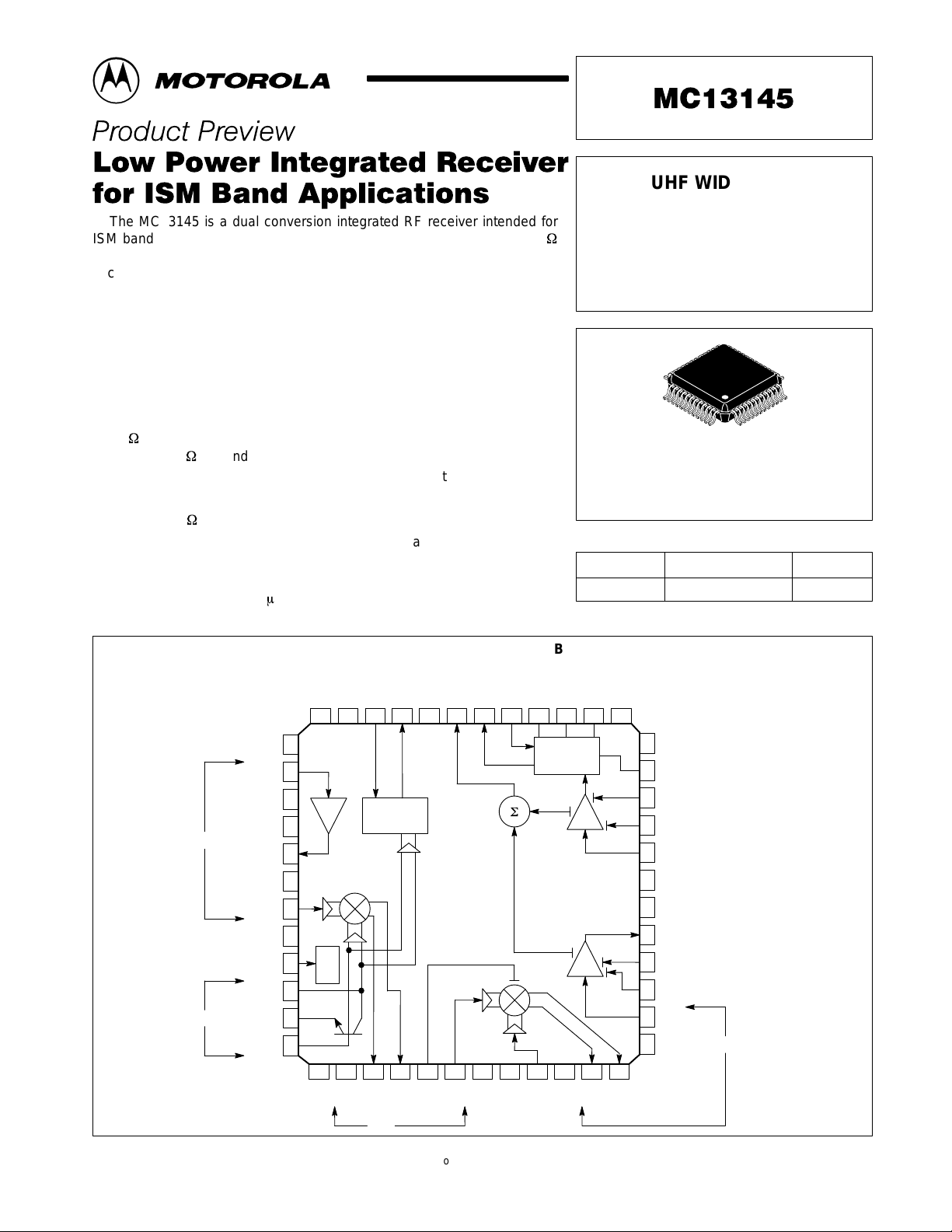
The MC13145 is a dual conversion integrated RF receiver intended for
ISM band applications. It features a Low Noise Amplifier (LNA), two 50
linear Mixers with linearity control, Voltage Controlled Oscillator (VCO),
second LO amplifier, divide by 64/65 dual modulus Prescalar, split IF
Amplifier and Limiter, RSSI output, Coilless FM/FSK Demodulator and
power down control. Together with the transmit chip (MC13146) and the
baseband chip (MC33410), a complete 900 MHz cordless phone system can
be implemented. This device may be used in applications within 2.0 GHz
since its RF bandwidth is greater than 2.4 GHz.
• Low (<1.8 dB @ 900 MHz) Noise Figure LNA with 14 dB Gain
• Externally Programmable Mixer linearity: IIP3 = 10(nom.) to +20 dBm
(Mixer1); IIP3 = 10 (nom.) to 20 dBm (Mixer2)
• 50
Mixer Input Impedance and Open Collector Output (Mixer 1 and
Mixer 2); 50 Second LO (LO2) Input Impedance
• Low Power 64/65 Dual Modulus Prescalar (MC12053 type)
• Split IF for Improved Filtering and Extended RSSI Range
• Internal 330
Terminations for 10.7 MHz Filters
• Linear Coilless FM/FSK Demodulator with Externally Programmable
Bandwidth, Center Frequency and Audio level
• 2.7 V to 6.5 V Operation, Low Current Drain (<30 mA @ 3.0 V) with
Power Down Mode (<1.0 A)
• 2.4 GHz RF , 1.0 GHz IF1 and 50 MHz IF2 Bandwidth
Order this document by MC13145/D
UHF WIDEBAND
RECEIVER SUBSYSTEM
(LNA, Mixer, VCO, Prescalar,
IF Subsystem,
Coilless Detector)
1
48
FTA SUFFIX
PLASTIC PACKAGE
CASE 932
(LQFP–48)
ORDERING INFORMATION
Device
XC13145FTA –40° to +85°C LQFP–48
Temperature Range
ESD Sensitive — Handle with Care
Package
RF
LO
V
EE
LNA In
V
EE
V
EE
LNA Out
V
EE
Mxr1In
Lin Adj1
Enable
oscC
oscE
oscB
PIN CONNECTIONS AND FUNCTIONAL BLOCK DIAGRAM
EE
VCCVCCMC
12 11 8 7 6 510 9
13
14
15
LNA
16
17
18
19
20
21
22
23
24
Control
25 26 29 30 31 3227 28
CC
V
PRSC Out
VEERSSI
/64, 65
EE
V
IF1+
IF1
IF1–
LinAdj2
2
Mxr In
Det Out
CC
V
Det Gain
EE
V
AFT
4321
Demod
33 34 35 36
LO2
AFT Buf
EE
V
Lim
IF
adj
F
IF2+
V
48
47
46
45
44
43
42
41
40
39
38
37
IF2–
V
EE
BWadj
Lim Dec2
Lim Dec1
Lim In
V
CC
V
CC
IF Out
IF Dec2
IF Dec1
IF In
V
EE
IF2
This document contains information on a product under development. Motorola
reserves the right to change or discontinue this product without notice.
MOTOROLA RF/IF DEVICE DATA
Motorola, Inc. 1998 Rev 0
1
Page 2
OVERALL RECEIVER SPECIFICA TIONS
Á
Á
Á
Á
Á
Á
Á
Á
Á
Á
Á
Unit
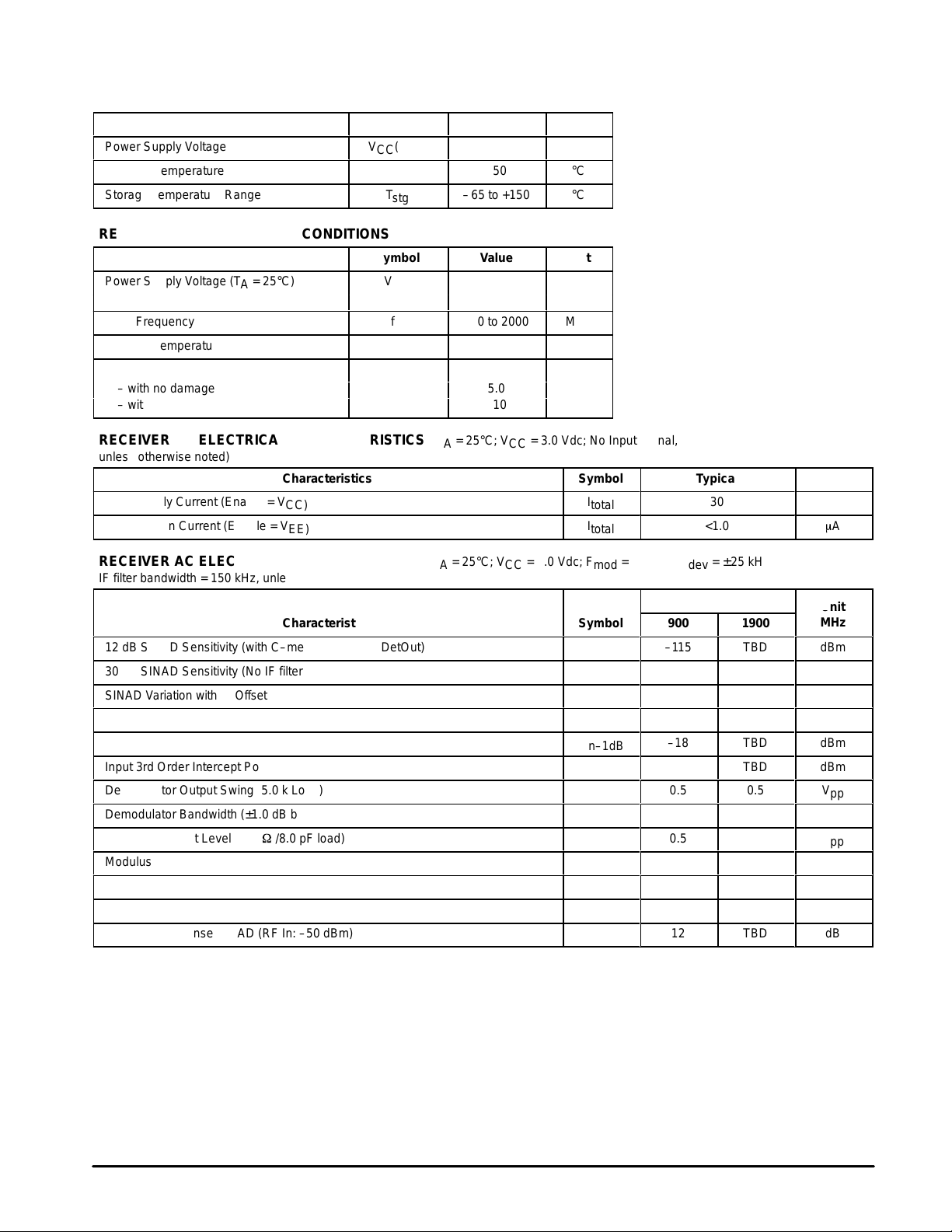
MAXIMUM RATINGS
Rating Symbol Value Unit
Power Supply Voltage
Junction Temperature
Storage Temperature Range
RECOMMENDED OPERATING CONDITIONS
Rating Symbol Value Unit
Power Supply Voltage (TA = 25°C)
Input Frequency
ББББББББББ
Ambient Temperature Range
ББББББББББ
Maximum Input Signal Level:
ББББББББББ
– with no damage
– with minor performance degradation
VCC(max)
ÁÁÁ
ÁÁÁ
ÁÁÁ
TJ(max)
T
stg
V
CC
V
EE
f
in
T
A
P
in
MC13145
7.0
150
–65 to +150
2.7 to 6.5
0
100 to 2000
ÁÁÁ
–40 to +85
ÁÁÁ
ÁÁÁÁÁÁ
5.0
–10
ÁÁ
ÁÁ
Vdc
°C
°C
Vdc
MHz
°C
dBm
RECEIVER DC ELECTRICAL CHARACTERISTICS (T
= 25°C; VCC = 3.0 Vdc; No Input Signal,
A
unless otherwise noted)
Characteristics
Total Supply Current (Enable = V
Power Down Current (Enable = V
RECEIVER AC ELECTRICAL CHARACTERISTICS (T
CC)
EE)
= 25°C; VCC = 3.0 Vdc; F
A
IF filter bandwidth = 150 kHz, unless otherwise noted)
Characteristics Symbol
12 dB SINAD Sensitivity (with C–message filter at DetOut)
30 dB SINAD Sensitivity (No IF filter distortion within ±40 kHz)
SINAD Variation with IF Offset of ±40 kHz (No IF filter distortion within ±40 kHz)
RSSI Dynamic Range
Input 1.0 dB Compression Point(Measured at IF output)
Input 3rd Order Intercept Point (Measured at IF output)
Demodulator Output Swing (5.0 k Load)
Demodulator Bandwidth (±1.0 dB bandwidth)
Prescalar Output Level (10 kW//8.0 pF load)
Modulus Control Input Level
SNR @ –30 dBm Signal Input (<25 kHz deviation;with C–Message Filter)
Total Harmonic Distortion (<25 kHz deviation;with C–Message Filter)
Spurious Response SINAD (RF In: –50 dBm)
Symbol Typical Unit
I
total
I
total
mod
P
in–1dB
IIP3
= 1.0 kHz; F
30
<1.0
= ±25 kHz;
dev
Typical
900 1900
–115
–100
5.0
80
–18
–8.0
0.5
100
0.5
0.5
50
1.0
12
TBD
TBD
TBD
TBD
TBD
TBD
0.5
100
0.5
0.5
TBD
TBD
TBD
mA
m
Unit
MHz
dBm
dBm
dB
dB
dBm
dBm
V
pp
kHz
V
pp
V
pp
dB
%
dB
A
2
MOTOROLA RF/IF DEVICE DATA
Page 3

INDIVIDUAL BLOCK SPECIFICATIONS
Unit
Unit
MC13145
LOW NOISE AMPLIFIER ELECTRICAL CHARACTERISTICS (T
Characteristics Symbol
Amplifier Gain
Noise Figure
1.0 dB Gain Compression Point
3rd Order Intercept Point
Reverse Isolation
Input Impedance (with externals)
Output Impedance (with externals)
Input Match (with externals)
Output Match (with externals)
LO1 to LNA Input Leakage
FIRST MIXER ELECTRICAL CHARACTERISTICS (T
Characteristics Symbol
Power Conversion Gain (Pin = –30 dBm)
Noise Figure
1.0 dB Gain Compression Point
3rd Order Intercept Point
Input Impedance (single–ended)
Output Impedance (differential with externals)
Input Match
Output Match (with externals)
RF to IF1 Leakage
LO to IF1 Leakage
LO to RF Leakage
Mixer Out to IF in Leakage
= 25°C; VCC = 3.0 Vdc, unless otherwise noted)
A
= 25°C; VCC = 3.0 Vdc, unless otherwise noted)
A
Typical
900 1900
S21
NF
P
in–1dB
IIP3
S12
S11
S22
Pgc
NF
P
in–1dB
IIP3
14
1.8
–8.0
–5.0
–35
50
50
15
15
–45
Typical
900 1900
0
13
–1.0
9.0
50
50
20
20
–38
–33
–33
–80
TBD
TBD
TBD
TBD
TBD
50
50
TBD
TBD
TBD
TBD
TBD
TBD
TBD
50
50
TBD
TBD
TBD
TBD
TBD
TBD
Unit
MHz
dB
dB
dBm
dBm
dB
W
W
dB
dB
dBm
Unit
MHz
dB
dB
dBm
dBm
W
W
dB
dB
dB
dBm
dBm
dB
SECOND MIXER ELECTRICAL CHARACTERISTICS (T
Characteristics
Noise Figure
1.0 dB Gain Compression Point
3rd Order Intercept Point
Input Impedance (single–ended)
Output Impedance (differential with externals)
Input Match
Output Match (with externals)
MOTOROLA RF/IF DEVICE DATA
= 25°C; VCC = 3.0 Vdc, unless otherwise noted)
A
Symbol Typical Unit
NF
P
in–1dB
IIP3
13
–1.0
9.0
50
330
20
20
dB
dBm
dBm
W
W
dB
dB
3
Page 4

MC13145
Unit
Unit
INDIVIDUAL BLOCK SPECIFICATIONS (continued)
LOCAL OSCILLATOR ELECTRICAL CHARACTERISTICS (T
Characteristics Symbol
LO Emitter Current (Enable = high)
Phase Noise @ 10 kHz Offset
Modulation Sideband
PRESCALAR ELECTRICAL CHARACTERISTICS (T
Characteristics Symbol
Divide Ratio
– MC = low
– MC = high
Output Impedance
Prescalar Output Level (10 kW//8pF load)
MC Input Level
MC Current Input (optional)
Prescalar Out to IF Amp and Lim Amp Input Leakage
= 25°C; VCC = 3.0 Vdc, unless otherwise noted)
A
= 25°C; VCC = 3.0 Vdc, unless otherwise noted)
A
IF AND LIMITING AMPLIFIERS ELECTRICAL CHARACTERISTICS (T
unless otherwise noted)
Characteristics
IF and Lim Amplifier Bandwidth
IF Amplifier Gain
IF Amplifier Noise Figure
IF Input & Output Impedance
IF Amp Input & Output Match
Limiting Amplifier Gain
Lim Amp Input Impedance
Lim Amp Input Match
IF Amp Output to Lim Amp Input Leakage (at 10.7 MHz)
RSSI Dynamic Range
RSSI Slope
RSSI Current Range
RSSI Response Time
Typical
900 1900
2.0
–80
–40
Typical
900 1900
65
64
50
0.5
0.5
200
–85
= 25°C; VCC = 3.0 Vdc,
A
Symbol Typical Unit
TBD
–75
TBD
65
64
50
0.5
0.5
200
TBD
40
40
7.0
330
20
85
330
15
80
80
0.5
0 to 40
1.0
Unit
MHz
mA
dBc/Hz
dBc
Unit
MHz
W
V
pp
V
pp
m
A
pp
dBm
MHz
dB
dB
W
dB
dB
W
dB
dB
dB
m
A/dB
m
A
m
s
COILLESS DEMODULATOR ELECTRICAL CHARACTERISTICS (T
unless otherwise noted)
Characteristics
Demodulator Output (at 25 kHz deviation)
Center Frequency
Frequency Adjust
Bandwidth Adjust
Output Impedance
Settling Time (assert Enable pin)
4
= 25°C; VCC = 3.0 Vdc,
A
Symbol Typical Unit
DetOut
0.5
10.7
<20
100 to 600
2000
TBD
MOTOROLA RF/IF DEVICE DATA
V
pp
MHz
MHz
kHz
W
ms
Page 5

MC13145
Figure 1. Application Diagram
LNAin
1.0 n
18
10 k
47 p
47 p
47 p
100 nH
2.55 n
6.8 n
6.8 n
390
100 p
47 p
MC
1.0 n
3.0 p
3.0 p
12 8 7
V
V
CC
CC
13
14
15
16
17
18
19
20
21
22
23
24
V
LNA
Control
CC
MC
64/65
1.0 n
50 k
9
PRSC Out
RSSI
S
MC13145
V
56 p
24 k
65432111 10
Det Out
CC
220 n
330 n
AFT
Det Gain
10 n
68 k
AFT Out
Fadj
BWadj
Lim
IF
2.7 k
V
CC
V
CC
PRSC Out
48
47
46
45
44
43
42
41
40
39
38
37
50 k
1.0 n
100 n
1.0 n
10M710M7
1.0 n
100 n
1.0 n
RSSI
Det Out
1.0
10 n
10 n
µ
D1*
33 k
V
Cont
1.0
µ
100 n 1.0 n 1.0
* D1 = MMBV809L
**T1 = Toko Part # 600ENAS–A998EK
9.1 p
25 26 29 30 31 3227 28 33 34 35 36
µ
1.0
16 p
V
CC
LD2 In
18
T1**
10 n
10 n
9.0 p
12 n
10 n
39 p
µ
2.7 H
µ
µ
2.7 H
510
10 n
150 p
1.0
µ
MOTOROLA RF/IF DEVICE DATA
5
Page 6

MC13145
OUTLINE DIMENSIONS
B
–AB–
–AC–
B1
9
–T–
4X
Z0.200 (0.008) AB T–U
DETAIL Y
A
A1
48
1
12
13
37
36
–U–
V1
25
24
–Z–
S1
S
4X
Z0.200 (0.008) AC T–U
G
BASE METAL
AD
N
J
FTA SUFFIX
PLASTIC PACKAGE
CASE 932–02
(LQFP)
ISSUE D
V
–T–, –U–, –Z–
0.080 (0.003) AC
TOP & BOTTOM
E
C
P
AE AE
DETAIL Y
_
M
NOTES:
1 DIMENSIONING AND TOLERANCING PER ANSI
Y14.5M, 1982.
2 CONTROLLING DIMENSION: MILLIMETER.
3 DATUM PLANE –AB– IS LOCATED AT BOTTOM OF
LEAD AND IS COINCIDENT WITH THE LEAD
WHERE THE LEAD EXITS THE PLASTIC BODY AT
THE BOTTOM OF THE PARTING LINE.
4 DATUMS –T–, –U–, AND –Z– TO BE DETERMINED
AT DATUM PLANE –AB–.
5 DIMENSIONS S AND V TO BE DETERMINED AT
SEATING PLANE –AC–.
6 DIMENSIONS A AND B DO NOT INCLUDE MOLD
PROTRUSION. ALLOWABLE PROTRUSION IS
0.250 (0.010) PER SIDE. DIMENSIONS A AND B DO
INCLUDE MOLD MISMATCH AND ARE
DETERMINED AT DATUM PLANE –AB–.
7 DIMENSION D DOES NOT INCLUDE DAMBAR
PROTRUSION. DAMBAR PROTRUSION SHALL
NOT CAUSE THE D DIMENSION TO EXCEED
0.350 (0.014).
8 MINIMUM SOLDER PLATE THICKNESS SHALL BE
0.0076 (0.0003).
9 EXACT SHAPE OF EACH CORNER IS OPTIONAL.
MILLIMETERS
DIMAMIN MAX MIN MAX
7.000 BSC 0.276 BSC
A1 3.500 BSC 0.138 BSC
B 7.000 BSC 0.276 BSC
B1 3.500 BSC 0.138 BSC
C 1.400 1.600 0.055 0.063
D 0.170 0.270 0.007 0.011
E 1.350 1.450 0.053 0.057
F 0.170 0.230 0.007 0.009
G 0.500 BASIC 0.020 BASIC
H 0.050 0.150 0.002 0.006
J 0.090 0.200 0.004 0.008
K 0.500 0.700 0.020 0.028
M 12 REF 12 REF
__
N 0.090 0.160 0.004 0.006
P 0.250 BASIC 0.010 BASIC
Q 1 5 1 5
R
____
R 0.150 0.250 0.006 0.010
S 9.000 BSC 0.354 BSC
S1 4.500 BSC 0.177 BSC
V 9.000 BSC 0.354 BSC
V1 4.500 BSC 0.177 BSC
W 0.200 REF 0.008 REF
X 1.000 REF 0.039 REF
INCHES
F
D
T–U
S
S
0.080 (0.003) Z
M
AC
SECTION AE–AE
Motorola reserves the right to make changes without further notice to any products herein. Motorola makes no warranty , representation or guarantee regarding
the suitability of its products for any particular purpose, nor does Motorola assume any liability arising out of the application or use of any product or circuit, and
specifically disclaims any and all liability, including without limitation consequential or incidental damages. “T ypical” parameters which may be provided in Motorola
data sheets and/or specifications can and do vary in different applications and actual performance may vary over time. All operating parameters, including “Typicals”
must be validated for each customer application by customer’s technical experts. Motorola does not convey any license under its patent rights nor the rights of
others. Motorola products are not designed, intended, or authorized for use as components in systems intended for surgical implant into the body, or other
applications intended to support or sustain life, or for any other application in which the failure of the Motorola product could create a situation where personal injury
or death may occur. Should Buyer purchase or use Motorola products for any such unintended or unauthorized application, Buyer shall indemnify and hold Motorola
and its officers, employees, subsidiaries, affiliates, and distributors harmless against all claims, costs, damages, and expenses, and reasonable attorney fees
arising out of, directly or indirectly, any claim of personal injury or death associated with such unintended or unauthorized use, even if such claim alleges that
Motorola was negligent regarding the design or manufacture of the part. Motorola and are registered trademarks of Motorola, Inc. Motorola, Inc. is an Equal
Opportunity/Affirmative Action Employer.
How to reach us:
USA/EUROPE/Locations Not Listed: Motorola Literature Distribution; JAPAN: Nippon Motorola Ltd.: SPD, Strategic Planning Office, 141,
P.O. Box 5405, Denver, Colorado 80217. 1–303–675–2140 or 1–800–441–2447 4–32–1 Nishi–Gotanda, Shagawa–ku, Tokyo, Japan. 03–5487–8488
Customer Focus Center: 1–800–521–6274
Mfax: RMFAX0@email.sps.mot.com – TOUCHTONE 1–602–244–6609 ASIA/PACIFIC: Motorola Semiconductors H.K. Ltd.; 8B Tai Ping Industrial Park,
Moto rola Fax Back Sys tem – US & Canada ONLY 1–800–774–1848 51 Ting Kok Road, Tai Po, N.T., Hong Kong. 852–26629298
HOME PAGE: http://motorola.com/sps/
– http://sps.motorola.com/mfax/
H
DETAIL AD
W
K
X
GAUGE PLANE
0.250 (0.010)
_
Q
Mfax is a trademark of Motorola, Inc.
6
◊
MOTOROLA RF/IF DEVICE DATA
MC13145/D
 Loading...