

Page 1
# "
"!
The MC13144 is designed in the Motorola High Frequency Bipolar
MOSIAC V wafer process to provide excellent performance in analog and
digital communication systems. It includes a cascoded LNA usable up to
2.0 GHz and at 1.8 Vdc, with 2 bit digital programming of the LNA bias.
Targeted applications are in the UHF Family Radio Services, UHF and
800 MHz Special Mobile Radio, 800 MHz Cellular and GSM, PCS, DECT
and PHS at 1.8 to 2.0 GHz and Cordless Telephones in the 902 to 928 MHz
band covered by FCC Title 47; Part 15. The MC13144 offers the following
features:
• 17 dB Gain at 900 MHz
• 1.4 dB Noise Figure at 900 MHz
• 1.0 dB Compression Point of –7.0 dBm; Input Third Order Intercept
Point of –5.0 dBm
• Low Operating Supply Voltage (1.8 to 6.0 Vdc)
• Programmable Bias with Enable 1 and Enable 2
• Enable 1 and Enable 2 Programmed High for Optimal Noise Figure and
Gain Associated with NF
• Can Override Enable and Externally Program In Up to 15 mA
Order this document by MC13144/D
VHF – 2.0 GHz LOW
NOISE AMPLIFIER WITH
PROGRAMMABLE BIAS
SEMICONDUCTOR
TECHNICAL DATA
8
1
D SUFFIX
PLASTIC PACKAGE
CASE 751
(SO–8)
MOSAIC V is a trademark of Motorola, Inc.
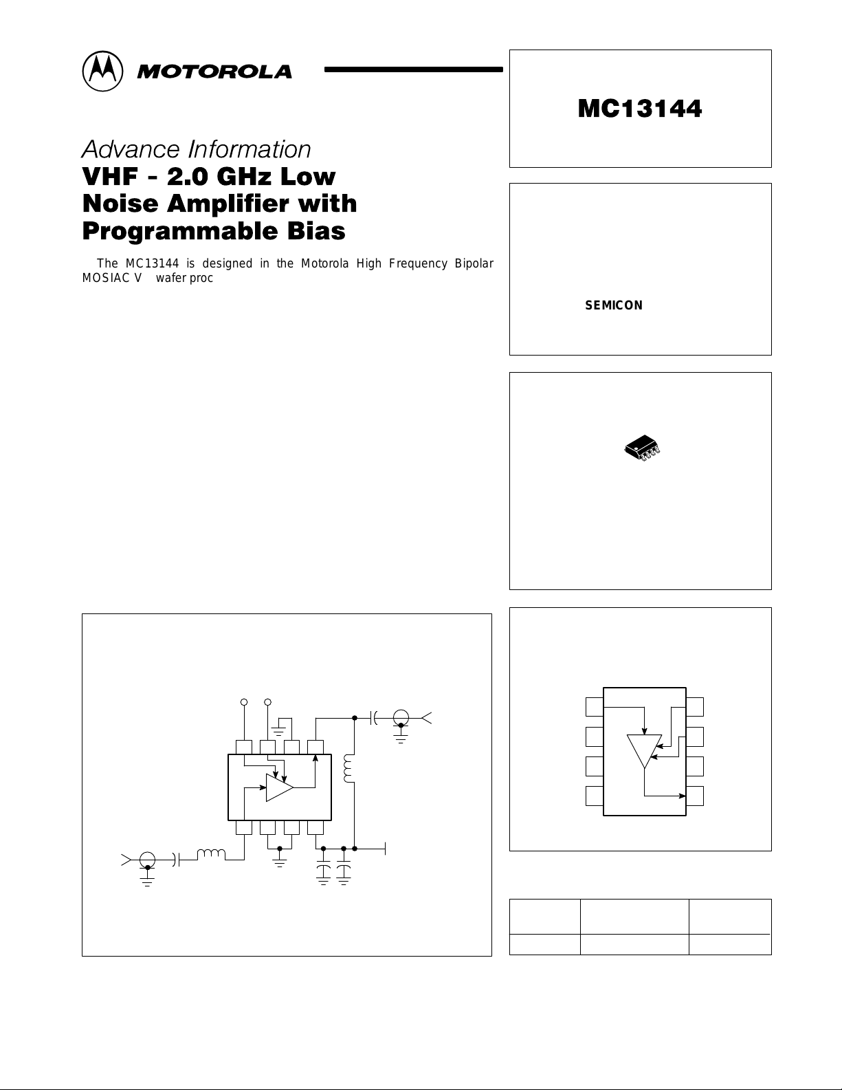
T ypical Application as 900 MHz Low Noise Amplifier
En2
En1
8
765
1234
RF
Input
47 p
5.6 nH
This device contains 67 active transistors.
1.6 p
8.2 nH
100 p100 n
PIN CONNECTIONS AND
FUNCTIONAL BLOCK DIAGRAM
1
RF
Output
V
CC
Device Package
MC13144D TA = – 40° to +85°C
In
V
2
EE
V
3
EE
V
4
CC
ORDERING INFORMATION
Operating
Temperature Range
En1
8
7
En2
V
6
EE
Out
5
SO–8
This document contains information on a new product. Specifications and information herein
are subject to change without notice.
MOTOROLA ANALOG IC DEVICE DATA
Motorola, Inc. 1997 Rev 0
1
Page 2
MC13144
MAXIMUM RATINGS
Power Supply Voltage
Junction Temperature
Storage Temperature Range
NOTES: 1. Devices should not be operated at or outside these values. The “Recommended Operating
Conditions” provide for actual device operation.
2.ESD data available upon request.
RECOMMENDED OPERATING CONDITIONS
Power Supply Voltage V
Rating Symbol Value Unit
Rating
VCC(max)
T
Jmax
T
stg
7.0
+150
–65 to +150
Symbol Min Typ Max Unit
CC
Vdc
°C
°C
1.8 – 6.0 Vdc
DC ELECTRICAL CHARACTERISTICS (T
Characteristic
Supply Current (Power Down) I
(En1 = En2 = Low)
Supply Current (Power Up) I
(En1 = High; En2 = Low)
Supply Current (Power Up) I
(En1 = High; En2 = Low)
Supply Current (Power Up) I
(En1 = High; En2 = Low)
AC ELECTRICAL CHARACTERISTICS (T
Characteristic
Amplifier Gain (50 Ω Insertion Gain) S
(En1 = En2 = High)
Amplifier Reverse Isolation S12 – –35 – dB
(En1 = En2 = High)
Amplifier Input Return Loss Γin
(En1 = En2 = High)
Amplifier Output Return Loss Γout
(En1 = En2 = High)
Input 3rd Order Intercept Point (En1 = En2 = High) IIP3 dBm
df = 100 kHz – –11 –
df = 1.0 MHz – –5.0 –
Amplifier Noise Figure NF – 1.4 2.0 dB
(Figure 1; En1 = En2 = High)
Amplifier Gain @ NF G
(Figure 1; En1 = En2 = High)
Amplifier Gain (En1 = En2 = High) G
Amplifier Gain G
(En1 = High; En2 = Low)
Amplifier Gain G
(En1 = High; En2 = Low)
= 25°C; VCC = 3.0 Vdc; fRF = 1.0 GHz; Pin = –25 dBm)
A
Symbol Min Typ Max Unit
CC0
CC1
CC2
CC3
= 25°C; VCC = 3.0 Vdc; fRF = 1.0 GHz; Pin = –25 dBm)
A
Symbol Min Typ Max Unit
2
21
amp
amp
NF
ain3
ain2
ain1
– 0.0001 20 µA
– 1.2 2.0 mA
– 3.4 5.0 mA
– 8.2 12 mA
– 12 – dB
– –10 – dB
– –15 – dB
– 17 – dB
14 17 – dB
10 13.3 – dB
6.0 9.2 – dB
2
MOTOROLA ANALOG IC DEVICE DATA
Page 3
MC13144
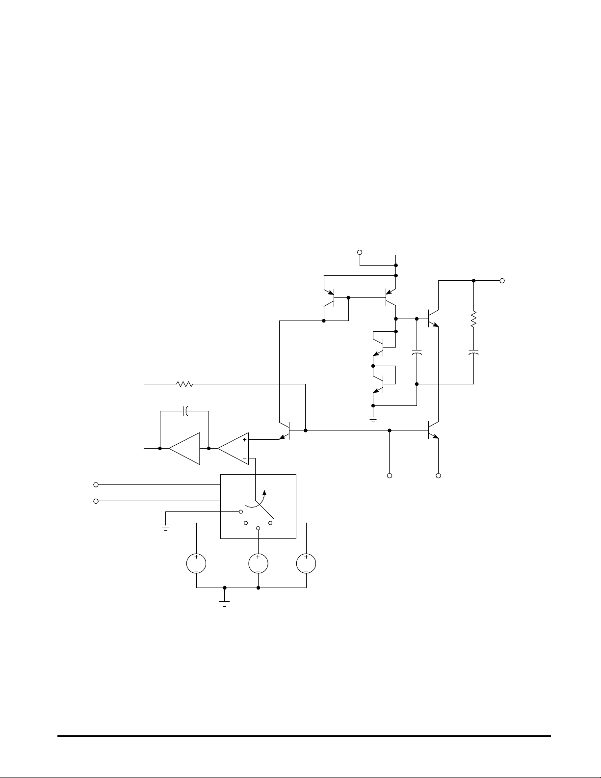
CIRCUIT DESCRIPTION
General
The MC13144 is a low noise amplifier with programmable
bias. This device is designated for use in the front end section
in analog and digital FM systems such as Wireless Local
Area Network (LAN), Digital European Cordless Telephone
(DECT), PHS, PCS, GPS, Cellular, UHF and 800 MHz
Special Mobile Radio (SMR), UHF Family Radio Services
and 902 to 928 MHz cordless telephones.
Current Regulation/Enable
Temperature compensating voltage independent current
regulation is digitally controlled by a 2 bit programmable
bias/enable circuit.
Figure 1. MC13144 Internal Circuit*
LNA
The LNA is a unique and patented cascode amplifier with
digitally (2 bit) programmable bias (see Internal Circuit
Schematic). Typical gain of the LNA is 17 dB for minimum
noise figure of 1.4 dB at 900 MHz.
Programmable Bias/Enable Circuit
This unique circuit allows for 3 bias levels and a standby
mode in which the LNA can be externally biased as desired.
4
V
CC
5
RF
Output
400
10 p
6
V
EE
–A
1 2, 3
En1
8
En2
7
V1
NOTE: * The MC13144 uses a unique and patent pending circuit topology.
V2
V3
RF In V
EE
MOTOROLA ANALOG IC DEVICE DATA
3
Page 4

MC13144
Á
Á
Á
Á
Á
Á
Á
Á
Á
Á
Á
ББББББ
ББББББ
ББББББ
ББББББ
APPLICATIONS INFORMATION
Evaluation PC Board
The evaluation PCB is very versatile and is intended to
be used across the entire useful frequency range of this
device. The PC board layout accommodates all SMT
components on the circuit side (see Circuit Side Component
Placement View).
Component Selection
The evaluation PC board is laid out for the 4DFA (2 pole
SMD Type) and 4DFB (3 pole SMD Type) filters which are
available for applications in Cellular and GSM, GPS (1.2 to
1.5 GHz), DECT, PHS and PCS (1.8 to 2.0 GHz) and
ISM Bands (902 to 928 MHz and 2.4 to 2.5 GHz). In the
926.5 MHz Application Circuit, a ceramic deielectric filter
is used (Toko part # 4DFA–926A10).
LNA Input/Output
The LNA input impedance is the base of a common emitter
cascode amplifier. The LNA output is the collector of the
cascode stage and it is loaded with a series resistor of 400 Ω
and a capacitor of 10 pF to provide stability .
Digitally Programmable Bias/Enable
The LNA is enabled by a 2 bit (En1 and En2)
programmable bias circuit. The internal circuit shows the
comparator circuit which programs the internal regulator. The
logic table below shows the bias and typical performance.
f = 1900 mHz
БББББ
ICC/Gain
БББББ
En1 Low
БББББ
En1 High
БББББ
БББББ
En2 Low
БББББ
0 mA/–22 dB
БББББ
3.4 mA/10 dB
БББББ
ÁÁÁÁ
En2 High
ÁÁÁÁ
1.2 mA/7.5 dB
ÁÁÁÁ
8.2 mA/13 dB
ÁÁÁÁ
Input/Output Matching
A typical application at 900 MHz yields 17 dB gain and
1.4 dB noise figure. In this circuit a series inductor of 5.6 nH
is used to match the input and a shunt inductor of 8.2 nH
which also serves as an RFC and a series capacitor of 0.9 p
is used to match the LNA output to 50 Ω load impedance.
It may be desirable to use a RF ceramic or SAW filter after
the LNA when driving a mixer to provide image frequency
rejection. The image filter is selected based on cost, size and
performance tradeoffs. Typical RF filters have 3.0 to 5.0 dB
insertion loss. Interface matching between the RF input, RF
filter and the mixer is shown in Application Circuit and the
Component Placement View.
A typical application at 1900 MHz yields 13 dB gain and
2.7 dB noise figure. In this circuit a series inductor of 5.6 nH
and a series capacitor of 1.0 pF are used to match the input
and a shut inductor of 2.0 nH and a series capacitor of 2.0 pF
are used to match the LNA output to 50 Ω load impedance.
f = 900 mHz
ÁÁÁÁ
ICC/Gain
ÁÁÁÁ
En1 Low
ÁÁÁÁ
En1 High
ÁÁÁÁ
RF
Input
БББББÁÁÁÁÁ
En2 Low
БББББ
0 mA/–22 dB
БББББ
3.4 mA/13 dB
БББББ
En2 High
ÁÁÁÁ
1.2 mA/9.2 dB
ÁÁÁÁ
9.4 mA/17 dB
ÁÁÁÁ
Figure 2. MC13144D Application Circuit
En1
V
47 p
CC
1.0 M
5.6 nH
En2
8
765
MC13144D
1234
(926.5 MHz)
100 p
8.2 nH
47
100 p100 n
39 nH 8.2 nH
Toko
Ceramic
Filter
0.4 p
V
CC
RF
Output
4
MOTOROLA ANALOG IC DEVICE DATA
Page 5

MC13144
Figure 3. T ypical S–Parameters VCC = 3.0 Vdc; En1 = En2 =1
Freq (MHz)
100 0.91 –11 4.2 143 0.00028 24 0.80 –10
125 0.92 –14 4.2 136 0.00033 71 0.79 –10
150 0.90 –16 4.2 127 0.0006 60 0.79 –1 1
175 0.89 –19 4.2 118 0.0011 80 0.78 –12
200 0.89 –22 4.0 108 0.0014 35 0.78 –13
250 0.88 –26 3.8 97 0.0015 39 0.78 –14
300 0.86 –32 4.1 77 0.0022 52 0.78 –17
350 0.85 –36 3.5 59 0.0017 65 .078 –19
400 0.84 –41 3.7 50 0.0024 68 0.79 –21
450 0.83 –46 3.7 26 0.0021 63 0.79 –24
500 0.81 –50 3.2 15 0.0028 56 0.79 –26
550 0.80 –55 3.5 –3.0 0.0027 51 0.80 –29
600 0.79 –59 3.1 –22 0.0038 46 0.81 –32
650 0.77 –63 3.0 –36 0.0057 30 0.82 –35
700 0.77 –67 2.8 –52 0.0067 32 0.83 –39
750 0.77 –72 2.5 –68 0.0095 26 0.83 –43
800 0.76 –77 2.2 –77 0.014 13 0.80 –49
850 0.74 –82 2.2 –86 0.019 12 0.75 –51
900 0.71 –85 2.3 –100 0.020 38 0.73 –51
950 0.69 –88 2.3 –117 0.021 55 0.74 –51
1000 0.67 –91 2.3 –132 0.020 72 0.76 –54
1100 0.67 –98 2.2 –163 0.022 87 0.76 –59
1200 0.66 –106 2.1 168 0.026 107 0.79 –65
1300 0.79 –72 1.9 136 0.030 134 0.64 –73
1400 0.64 –121 1.9 100 0.038 150 0.80 –80
1500 0.62 –128 1.9 74 0.053 170 0.81 –87
1600 0.61 –135 1.7 40 0.068 157 0.82 –96
1700 0.59 –145 1.5 7.0 0.076 120 0.81 –105
1800 0.58 –152 1.4 –24 0.092 97 0.80 –115
1900 0.54 –125 1.2 –57 0.11 59 0.74 –125
2000 0.47 –130 1.0 –79 0.093 195 0.68 –130
S11 Mag S11 Ang S21 Mag S21 Ang S12 Mag S12 Ang S22 Mag S22 Ang
MOTOROLA ANALOG IC DEVICE DATA
5
Page 6

MC13144
Figure 4. Circuit Side Component Placement View
MC13144D Rev 0
E2
T oko Ceramic
Filter
E1
1.0 M
MC13144D
5.6 nH
47 p
39 nH
100 p
100 p
8.2 nH
47
100 n
LNA
In
Figure 5. Circuit Side View
E2
8.2 nH
0.4 p
LNA
Out
V
CC
MC13144D Rev 0
E1
LNA
Out
LNA
In
NOTES: Critical dimensions are 50 MIL centers lead to lead in SO–8 footprint.
Also line widths to labeled ports excluding VCC, E1 and E2 are 50 MIL (0.050 inch).
FR4 PCB, 1/32 inch.
6
V
CC
MOTOROLA ANALOG IC DEVICE DATA
Page 7

E1
MC13144
Figure 6. Ground Side View
LNA In
V
CC
LNA Out
C
A
E
B
A1
E2
NOTES: FR4 PCB, 1/32 inch.
MC13144D Rev 0
OUTLINE DIMENSIONS
D SUFFIX
PLASTIC PACKAGE
CASE 751–06
(SO–8)
ISSUE T
D
58
0.25MB
1
H
4
e
M
h
X 45
_
q
C
A
SEATING
PLANE
0.10
L
B
SS
A0.25MCB
NOTES:
1. DIMENSIONING AND TOLERANCING PER ASME
Y14.5M, 1994.
2. DIMENSIONS ARE IN MILLIMETER.
3. DIMENSION D AND E DO NOT INCLUDE MOLD
PROTRUSION.
4. MAXIMUM MOLD PROTRUSION 0.15 PER SIDE.
5. DIMENSION B DOES NOT INCLUDE DAMBAR
PROTRUSION. ALLOWABLE DAMBAR
PROTRUSION SHALL BE 0.127 TOTAL IN EXCESS
OF THE B DIMENSION AT MAXIMUM MATERIAL
CONDITION.
MILLIMETERS
DIM MIN MAX
A 1.35 1.75
A1 0.10 0.25
B 0.35 0.49
C 0.19 0.25
D 4.80 5.00
E
3.80 4.00
1.27 BSCe
H 5.80 6.20
h
0.25 0.50
L 0.40 1.25
0 7
q
__
MOTOROLA ANALOG IC DEVICE DATA
7
Page 8

MC13144
Motorola reserves the right to make changes without further notice to any products herein. Motorola makes no warranty , representation or guarantee regarding
the suitability of its products for any particular purpose, nor does Motorola assume any liability arising out of the application or use of any product or circuit, and
specifically disclaims any and all liability, including without limitation consequential or incidental damages. “T ypical” parameters which may be provided in Motorola
data sheets and/or specifications can and do vary in different applications and actual performance may vary over time. All operating parameters, including “Typicals”
must be validated for each customer application by customer’s technical experts. Motorola does not convey any license under its patent rights nor the rights of
others. Motorola products are not designed, intended, or authorized for use as components in systems intended for surgical implant into the body, or other
applications intended to support or sustain life, or for any other application in which the failure of the Motorola product could create a situation where personal injury
or death may occur. Should Buyer purchase or use Motorola products for any such unintended or unauthorized application, Buyer shall indemnify and hold Motorola
and its officers, employees, subsidiaries, affiliates, and distributors harmless against all claims, costs, damages, and expenses, and reasonable attorney fees
arising out of, directly or indirectly, any claim of personal injury or death associated with such unintended or unauthorized use, even if such claim alleges that
Motorola was negligent regarding the design or manufacture of the part. Motorola and are registered trademarks of Motorola, Inc. Motorola, Inc. is an Equal
Opportunity/Affirmative Action Employer.
How to reach us:
USA/EUROPE /Locations Not Listed: Motorola Literature Distribution; JAPAN: Nippon Motorola Ltd.: SPD, Strategic Planning Office, 4–32–1,
P.O. Box 5405, Denver, Colorado 80217. 1–303–675–2140 or 1–800–441–2447 Nishi–Gotanda, Shinagawa–ku, Tokyo 141, Japan. 81–3–5487–8488
Customer Focus Center: 1–800–521–6274
Mfax: RMFAX0@email.sps.mot.com – TOUCHTONE 1–602–244–6609 ASIA/PACIFIC: Motorola Semiconductors H.K. Ltd.; 8B Tai Ping Industrial Park,
Moto rola Fax Back System – US & Canada ONLY 1–800–774–1848 51 Ting Kok Road, Tai Po, N.T., Hong Kong. 852–26629298
HOME PAGE: http://motorola.com/sps/
8
– http://sps.motorola.com/mfax/
◊
MOTOROLA ANALOG IC DEVICE DATA
Mfax is a trademark of Motorola, Inc.
MC13144/D
 Loading...