

Page 1
Order this document By MC13142/D
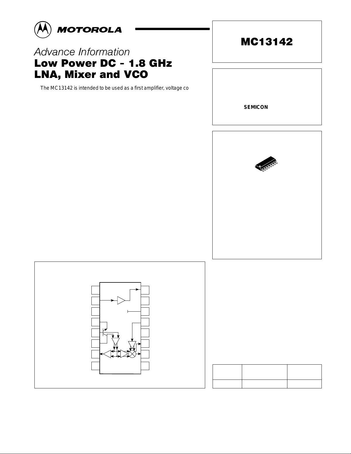
The MC13142 is intended to be used as a first amplifier, voltage controlled
oscillator and down converter for RF applications. It features wide band
operation, low noise, high gain and high linearity while maintaining low
current consumption. The circuit consists of a Low Noise Amplifier (LNA), a
Voltage Controlled Oscillator (VCO), a buf fered oscillator output, a mixer, an
Intermediate Frequency amplifier (IF
mixer IF bandwidth allows this part also to be used as an up converter and
exciter amplifier.
• Wide RF Bandwidth: DC–1.8 GHz
• Wide LO Bandwidth: DC–1.8 GHz
• Wide IF Bandwidth: DC–1.8 GHz
• Low Power: 13 mA @ V
• High Mixer Linearity: P
= 2.7 – 6.5 V
CC
i1.0 dB
= 3.0 dBm
• Linearity Adjustment Increases IP
• Single–Ended 50 Ω Mixer Input
• Double Balanced Mixer Operation
• Open Collector Mixer Output
• Single Transistor Oscillator with Collector, Base and Emitter Pinned Out
• Buffered Oscillator Output
) and a dc control section. The wide
amp
Up to 20 dBm
3in
LOW POWER DC – 1.8 GHz
LNA, MIXER and VCO
SEMICONDUCTOR
TECHNICAL DATA
16
1
D SUFFIX
PLASTIC PACKAGE
CASE 751B
(SO–16)
PIN CONNECTIONS
SO–16
EN
1
RF
2
in
V
3
EE
Osc E
4
Osc B
5
Osc C, V
This device contains 176 active transistors.
This document contains information on a new product. Specifications and information herein
are subject to change without notice.
MOTOROLA RF/IF DEVICE DATA
V
CC
Buff
CC
6
7
8
Mx Lin
Cont
RF
16
V
15
CC
Mix Lin Cont
14
RF
13
V
EE
12
IF+
11
IF–
10
9
V
EE
out
m
ORDERING INFORMATION
Operating
Device
MC13142D TA = –40° to +85°C SO–16
Motorola, Inc. 1998 Rev 1
Temperature Range
Package
1
Page 2
MC13142
A
mA
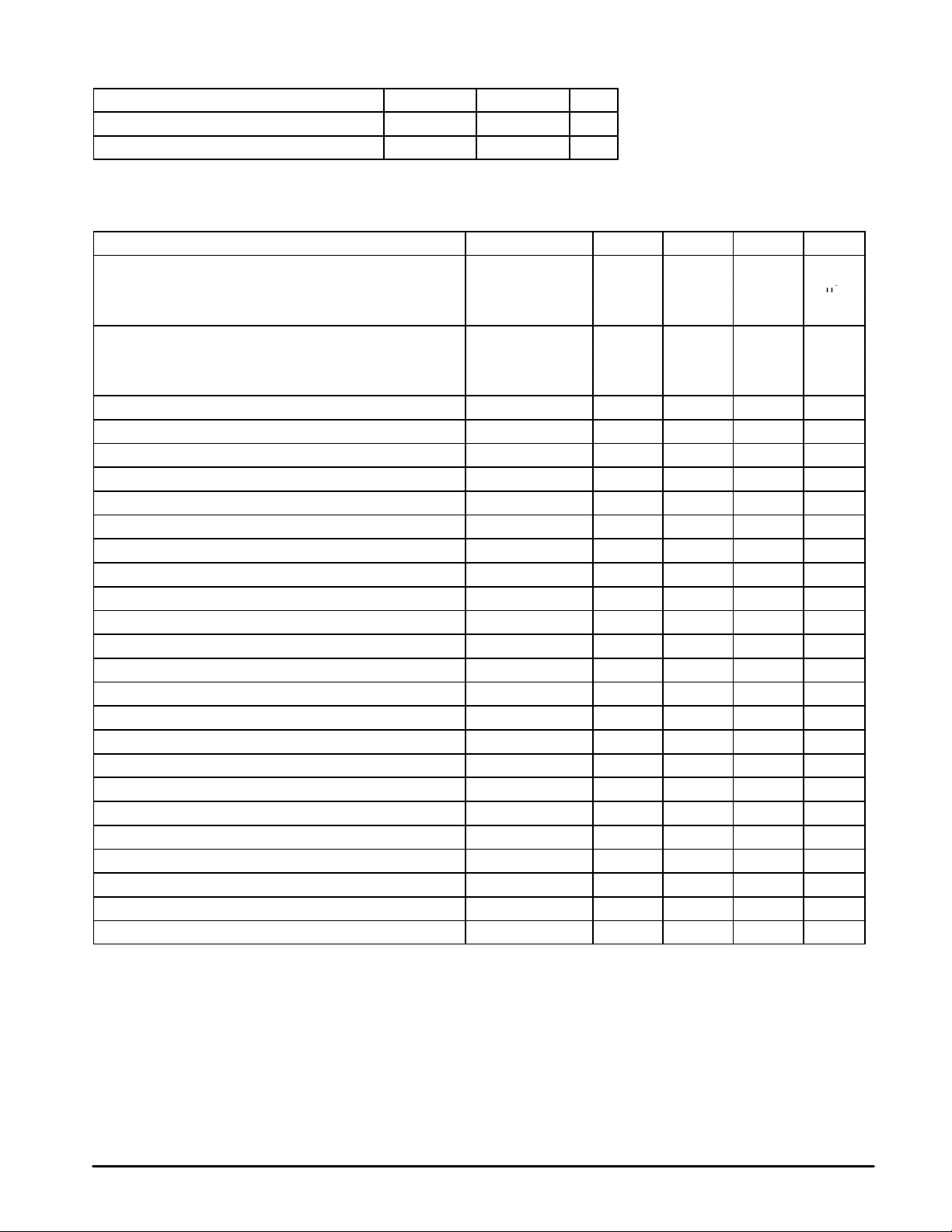
MAXIMUM RATINGS (T
Power Supply Voltage V
Operating Supply Voltage Range V
NOTE: ESD data available upon request.
ELECTRICAL CHARACTERISTICS (V
Supply Current (Disable) I
Pin 15 with Pin 1 @ 0 V I
Pin 10 and 11 with Pin 1 @ 0 V I
Pin 6 with Pin 1 @ 0 V I
Supply Current (Enable) I
Pin 15 with Pin 1 @ 3.0 V I
Pin 10 with Pin 1 @ 3.0 V I
Pin 6 with Pin 1 @ 3.0 V I
Amplifier Gain (50 Ω Insertion Gain) S
Amplifier Reverse Isolation S
Amplifier Input Match Γin
Amplifier Output Match Γ
Amplifier 1.0 dB Gain Compression Pin
Amplifier Input Third Order Intercept IP3
Amplifier Noise Figure (Application Circuit) NF 1.0 1.8 4.0 dB
Amplifier Gain @ N.F. G
Mixer Voltage Conversion Gain (RP = RL = 800 Ω) VG
Mixer Power Conversion Gain (RP = RL = 800 Ω) PG
Mixer Input Match Γin
Mixer SSB Noise Figure NF
Mixer 1.0 dB Gain Compression Pin
Mixer Input Third Order Intercept IP3
Oscillator Buffer Drive (50 Ω) P
Oscillator Phase Noise @ 25 kHz Offset N
RFin Feedthrough to RF
RF
Feedthrough to RF
out
LO Feedthrough to IF P
LO Feedthrough to RF
LO Feedthrough to RF
Mixer RF Feedthrough to IF P
Mixer RF Feedthrough to RF
= 25°C, unless otherwise noted.)
A
Rating
= 3.0 V, TA = 25°C, LOin = –10 dBm @ 950 MHz, IF @ 50 MHz.)
CC
Characteristic Symbol Min Typ Max Unit
m
m
in
m
in
Symbol Value Unit
CC(max)
CC
7.0 Vdc
2.7 to 6.5 Vdc
CC_Total
CC_15
CC_Mix
CC_6
CC_Total
CC_15
CC_Mix
CC_6
21
12
amp
out amp
–1.0 dB
in
NF
C
C
M
SSBM
–1.0 dBM
InM
VCO
Φ
P
RFin–RFm
P
RFout–RFm
LO–IF
P
LO–RFin
P
LO–RFm
RFm–IF
P
RFm–RFin
–230 – 230
–110 – 110
–20 – 20
–100 – 100
8.25 13.5 26
1.0 – 4.5
1.25 – 7.5
6.0 – 14
6.5 12 13 dB
– –33 – dB
– –10 – dB
– –15 – dB
–18 –15 –8.0 dBm
– –5.0 – dBm
– 17 – dB
– 9.0 – dB
–7.0 –3.0 –2.0 dB
– –20 – dB
– 12 – dB
– 3.0 – dBm
– –1.0 – dBm
–19.5 –16 –12 dBm
– –90 – dBc/Hz
– –35 – dB
– –35 – dB
– –35 – dBm
– –35 – dBm
– –35 – dBm
– –25 – dB
– –25 – dB
µ
2
MOTOROLA RF/IF DEVICE DATA
Page 3

MC13142
CIRCUIT DESCRIPTION
General
The MC13142 is a low power LNA, double–balanced
Mixer, and VCO. This device is designated for use as the
frontend section in analog and digital FM systems such as
Digital European Cordless Telephone (DECT), PHS, PCS,
Cellular, UHF and 800 MHz Special Mobile Radio (SMR),
UHF Family Radio Services and 902 to 928 MHz cordless
telephones. It features a mixer linearity control to preset or
auto program the mixer dynamic range, an enable function
and a wideband IF so the IC may be used either as a down
converter or an up converter. Further details are covered in
the Pin by Pin Description which shows the equivalent
internal circuit and external circuit requirements.
Current Regulation/Enable
Temperature compensating voltage independent current
regulators are controlled by the enable function in which
“high” powers up the IC.
Low Noise Amplifier (LNA)
The LNA is internally biased at low supply current
(approximately 2.0 mA emitter current) for optimal noise
figure and gain. The LNA output is biased internally with a
600 Ω resistor to VCC. Input and output matching may be
achieved at various frequencies using few external
components. Matching the LNA for Maximum stable gain
(MSG) yields noise performance within a few tenths of a dB
of the minimum noise figure.
Mixer
The mixer is a double–balanced four quadrant multiplier
biased class AB allowing for programmable linearity control
via an external current source. An input third order intercept
point of 20 dBm may be achieved. All 3 ports of the mixer are
designed to work up to 1.8 GHz. The mixer has a 50 Ω
single–ended RF input and open collector differential IF
outputs. An on–board Local Oscillator transistor has the
emitter, base and collector pinned out to implement a low
phase noise VCO in various configurations. Additionally, a
buffered LO output is provided for operation with a frequency
synthesizer. The linear gain of the mixer is approximately
0 dB with a SSB noise figure of 12 dB in the IF output circuit
configuration shown in the application example.
Local Oscillator
The on–chip transistor operates with coaxial transmission
line or LC resonant elements to over 2.0 GHz. Biasing is
done with a temperature compensated current source in the
emitter and a collector to base internal resistor of 7.6 kΩ;
however, an RFC from VCC to base is recommended. The
application circuit shows a voltage controlled Clapp oscillator
operating at center frequency of 975 MHz.
MOTOROLA RF/IF DEVICE DATA
3
Page 4
MC13142
Á
Á
Á
Á
Á
Á
Á
Á
Á
Á
Á
Á
Á
Á
Á
Á
Á
Á
Á
Á
Á
Á
Á
Á
Á
Á
Á
Á
Á
Á
Á
Á
Á
Á
Á
Á
Á
Á
Á
Á
Á
Á
RF
V
Á
Á
Á
Á
Á
Á
Á
Á
Á
Á
Á
Á
Á
Á
Á
Á
Á
Á
Á
Á
Á
Á
Á
Á
Á
Á
Á
Á
Á
Á
Á
Á
Á
Á
Á
Á
Á
Osc C
Á
Á
Á
Á
Á
Á
Á
Á
Á
Á
Á
Á
Á
LO Buf
Á
Á
Á
Á
Pin
16 Pin
SOIC
1
ÁÁÁ
ÁÁÁ
ÁÁÁ
ÁÁÁ
ÁÁÁ
ÁÁÁ
ÁÁÁ
ÁÁÁ
ÁÁÁ
ÁÁÁ
2
ÁÁÁ
ÁÁÁ
3
ÁÁÁ
ÁÁÁ
ÁÁÁ
16
ÁÁÁ
ÁÁÁ
Symbol
EN
ÁÁ
ÁÁ
ÁÁ
ÁÁ
ÁÁ
ÁÁ
ÁÁ
ÁÁ
ÁÁ
ÁÁ
RF
in
ÁÁ
ÁÁ
V
EE
ÁÁ
ÁÁ
ÁÁ
RF
out
ÁÁ
ÁÁ
PIN FUNCTION DESCRIPTION
Equivalent Internal Circuit
(20 Pin LQFP)
V
CC
40 k1
2.0 V
V
CC
70 k
2.0 V
ref2
V
EE
RF
V
EN
16
out
2
in
3
EE
BE
BE
Description
Enable, E Osc
In SO–16, both enables, (for the Oscillator/LO Buffer and
БББББББББББББ
LNA/Mixer) are bonded to Pin 1. Enable by pulling up to
VCC or to greater than 2.0 VBE.
БББББББББББББ
БББББББББББББ
БББББББББББББ
БББББББББББББ
БББББББББББББ
БББББББББББББ
БББББББББББББ
БББББББББББББ
БББББББББББББ
V
CC
600
RF Input
The input is the base of an NPN low noise amplifier.
БББББББББББББ
Minimum external matching is required to optimize the
input return loss and gain.
БББББББББББББ
VEE – Negative Supply
VEE pin is taken to an ample dc ground plane through a
БББББББББББББ
low impedance path. The path should be kept as short
as possible. A two sided PCB is implemented so that
БББББББББББББ
ground returns can be easily made through via holes.
БББББББББББББ
RF Output
The output is from the collector of the LNA; it is internally
БББББББББББББ
biased with a 600 Ω resistor to VCC. As shown in the 926
MHz application receiver the output is conjugately
БББББББББББББ
matched with a shunt L, and series L and C network.
2.0 mA
V
ref3
ÁÁÁ
ÁÁÁ
ÁÁÁ
ÁÁÁ
ÁÁÁ
ÁÁÁ
ÁÁÁ
ÁÁÁ
ÁÁÁ
ÁÁÁ
ÁÁÁ
ÁÁÁ
ÁÁÁ
ÁÁÁ
ÁÁÁ
4
5
6
6
8
7
4
Osc E
ÁÁ
Osc B
Osc C
ÁÁ
ÁÁ
ÁÁ
ÁÁ
ÁÁ
V
CC
V
CC
ÁÁ
ÁÁ
ÁÁ
ÁÁ
ÁÁ
LO Buff
ÁÁ
ÁÁ
ÁÁ
ÁÁ
4
Osc E
5
Osc B
6
Osc C
6
V
CC
V
7.6 k
7
8
CC
On–Board VCO Transistor
БББББББББББББ
10
The transistor has the emitter, base and collector + V
pins available. Internal biasing which is compensated for
БББББББББББББ
stability over temperature is provided. It is recommended
БББББББББББББ
that the base pin is pulled up to VCC through an RFC
1.5
mA
V
EE
chosen for the particular oscillator center frequency. The
БББББББББББББ
application circuit shows a modified Colpitts or Clapp
БББББББББББББ
oscillator configuration and its design is discussed in
detail in the application section.
БББББББББББББ
CC
Supply Voltage (VCC)
V
EE
V
CC
Two VCC pins are provided for the Local Oscillator and
БББББББББББББ
LO Buffer Amplifier. The operating supply voltage range
БББББББББББББ
is from 2.7 Vdc to 6.5 Vdc. In the PCB layout, the V
trace must be kept as wide as feasible to minimize
БББББББББББББ
inductive reactances along the trace. VCC should be
БББББББББББББ
decoupled to VEE at the IC pin as shown in the
component placement view.
БББББББББББББ
CC
Local Oscillator Buffer
1.0
mA
V
EE
This is a buffered output providing –16 dBm
БББББББББББББ
(50 Ω termination) to drive the fin pin of a PLL
БББББББББББББ
synthesizer. Impedance matching to the synthesizer may
be necessary to deliver the optimal signal and to
БББББББББББББ
improve the phase noise performance of the VCO.
БББББББББББББ
MOTOROLA RF/IF DEVICE DATA
Page 5
Pin
Á
Á
Á
Á
Á
Á
Á
Á
Á
Á
Á
Á
Á
Á
Á
Á
Á
Á
Á
Á
Á
Á
Á
Á
Á
Á
Á
Á
Á
Á
Á
Á
Á
Á
Á
Á
Á
Á
Á
Á
Á
Á
Á
Á
Á
Á
Á
Á
Á
Á
Á
Á
Á
Á
Á
Á
Á
Á
Á
Á
Á
Á
Á
Á
Á
Á
16 Pin
SOIC
9, 12
ÁÁÁ
ÁÁÁ
ÁÁÁ
10, 11
ÁÁÁ
ÁÁÁ
ÁÁÁ
ÁÁÁ
ÁÁÁ
Symbol
Symbol
V
EE
ÁÁ
ÁÁ
ÁÁ
IF–, IF+
ÁÁ
ÁÁ
ÁÁ
ÁÁ
ÁÁ
PIN FUNCTION DESCRIPTION (continued)
Equivalent Internal Circuit
Equivalent Internal Circuit
(20 Pin LQFP)
(20 Pin LQFP)
10
IF–
9
V
V
CC
EE
11
IF+
12
V
EE
MC13142
V
CC
Description
Description
VEE, Negative Supply
These pins are VEE supply for the mixer IF output. In the
БББББББББББББ
application PC board these pins are tied to a common
VEE trace with other VEE pins.
БББББББББББББ
БББББББББББББ
IF Output
The IF is a differential open collector configuration which
БББББББББББББ
designed to use over a wide frequency range for up
conversion as well as down conversion. Differential to
БББББББББББББ
single–ended circuit configuration and matching options
БББББББББББББ
are discussed in the application section. 6.0 dB of
additional Mixer gain can be achieved by conjugately
БББББББББББББ
matching at the desired IF frequency.
БББББББББББББ
13
ÁÁÁ
ÁÁÁ
ÁÁÁ
ÁÁÁ
ÁÁÁ
ÁÁÁ
14
ÁÁÁ
ÁÁÁ
ÁÁÁ
ÁÁÁ
ÁÁÁ
ÁÁÁ
ÁÁÁ
ÁÁÁ
15 V
RF
m
ÁÁ
ÁÁ
ÁÁ
ÁÁ
ÁÁ
ÁÁ
Mix Lin
ÁÁ
Cont
ÁÁ
ÁÁ
ÁÁ
ÁÁ
ÁÁ
ÁÁ
ÁÁ
CC
13
RF
m
14
Mix Lin
Cont
15
V
CC
V
CC
V
ref1
V
EE
33
The mixer input impedance is broadband 50 Ω for
БББББББББББББ
applications up to 1.8 GHz. It easily interfaces with a RF
БББББББББББББ
ceramic filter as shown in the application schematic.
БББББББББББББ
БББББББББББББ
БББББББББББББ
БББББББББББББ
Mixer Linearity Control
Mixer RF Input
БББББББББББББ
The mixer linearity control circuit accepts approximately
0 to 2.3 mA control current to set the dynamic range of
БББББББББББББ
the mixer. An Input Third Order Intercept Point, IIP3 of
БББББББББББББ
20 dBm may be achieved at 2.3 mA of control current
(approximately 7.0 mA of additional supply current).
БББББББББББББ
БББББББББББББ
БББББББББББББ
БББББББББББББ
БББББББББББББ
400
33
µ
A
VCC, Power Supply
V
CC
MOTOROLA RF/IF DEVICE DATA
5
Page 6

MC13142
APPLICATIONS INFORMATION
Evaluation PC Board
The evaluation PCB is very versatile and is intended to be
used across the entire useful frequency range of this device.
The PC board accommodates all SMT components on the
circuit side (see Circuit Side Component Placement View).
This evaluation board will be discussed and referenced in
this section.
Figure 1. Application Circuit
(926.5 MHz)
PC Rotary SW
SMA
µ
33 k
V
CC
Output
47 p
3.0 p
3.9 p
5.6 p
*ZO =
Ω
50
47 p
MMBV809
100 n
100 p
6.8 nH
2.55 nH
100 p
ZO = 50
2.4 p
2.4 p
390 nH
1
LNA
Ω
2
3
4
5
6
7
8
VCO
LO Buffer
RF
Input
V
Control
120 k
100 n
1.0
LO Buffer
Component Selection
The evaluation PC board is designed to accommodate
specific components, while also being versatile enough to
use components from various manufacturers. The circuit
side placement view is illustrated for the components
specified in the application circuit. The application circuit
schematic specifies particular components that were used to
achieve the results given and specified in the tables but
alternate components of the same Q and value should give
equivalent results.
V
CC
51
Enable
39 nH
100 p
18 nH
V
CC
3.6 p
2.3 mA
Max
Z Transformer
16:1
Toko RF
Filter
L
C
SMA
DC Bias
Mixer Linearity
Control
Mixer
IF
Outputs
16
15
14
13
12
11
10
9
IF
Output
SMA
6
NOTE: *50 Ω Microstrip Transmission Line; length shown in Figure 2.
MOTOROLA RF/IF DEVICE DATA
Page 7

MC13142D
Rev A
MC13142
Figure 2. 900 MHz Circuit Side Component Placement View
Mix In
Mix Lin Cont
3.6 p
LNA
Output
LNA
Input
47 p
3.0 p
T oko
926A10
Dielectric
Filter
Rotary
Switch
V–Cont
3.9 p
100 p
18 nH
51PC
6.8 nH
39 nH
100 n
1.0
µ
MC13142D
2.4 p
5.6 p
33 k120 k
2.4 p
390 nH
2.55 nH
5.6 p
91 p
MMBV809
16:1
Impedance
Transformer
1.0
100 n
µ
V
CC
C
L
IF
Out
100 p
LO
Buf
Out
NOTES: The PCB is laidout for the 4DFA (2 pole SMD type) and 4DFB (3 pole SMD type) filters which are available for applications in
cellular and GSM,GPS (1.2–1.5 GHz), DECT, PHS and PCS (1.8–2.0 GHz) and ISM Bands (902–928 MHz and 2.4–2.5 GHz).
In the component placement shown above, the 926.5 MHz dielectric type image filter is used (T oko Part # 4DFA–926A10).
The PCB also accommodates a surface mount SAW filter in an eight or six pin ceramic package for the cellular base and
handset frequencies. Recommended manufacturers are Siemens and Murata.
Traces are provided on the PCB to evaluate the LNA and mixer separately. The component placement view shows external
circuit components used for the 926.5 MHz application circuit. Note: some traces must be cut to accommodate placement of
components; likewise some traces must be shorted. The voltage controlled oscillator is shown with the varactor referenced to
VEE ground. The PCB is modified as shown to do this.
16:1 broadband impedance transformer is mini circuits part #TX16–R3T; it is in the leadless surface mount “TX” package.
Components L and C comprise a low pass filter used to provide narrowband matching at a given IF frequency. For example at
49 MHz C = 36 p and L = 330 nH.
The microstrip trace on the ground side of the PCB is intended for a microstrip resonator; it is cut free when using a lump
inductor as done above.
MOTOROLA RF/IF DEVICE DATA
7
Page 8

MC13142
Input Matching/Components
It is desirable to use a RF ceramic or SAW filter before the
mixer to provide image frequency rejection. The filter is
selected based on cost, size and performance tradeoffs.
Typical RF filters have 3.0 to 5.0 dB insertion loss. The PC
board layout accommodates both ceramic and SAW RF
filters which are offered by various suppliers such as
Siemens, Toko and Murata.
Interface matching between the LNA, RF filter and the
mixer will be required. The interface matching networks
shown in the application circuit are designed for 50 Ω
interfaces.
In the application circuit, the LNA is conjugately matched
to 50 Ω input and output for 3.0 to 5.0 Vdc VCC. 17 dB gain
and 1.8 dB noise figure is typical at 926 MHz. The mixer
measures 0 dB gain and 12 dB noise figure as shown in the
application circuit. Typical insertion loss of the Toko ceramic
filter is 3.0 dB. Thus, the overall gain of the frontend receiver
is 14 dB with a 3.3 dB noise figure.
System Noise Considerations
The block diagram shows the cascaded noise stages of
the MC13142 in the frontend receiver subsystem; it
Figure 3. Frontend Subsystem Block Diagram for Noise Analysis
represents the application circuit. In the cascaded noise
analysis the system noise equation is:
Fsystem = F1 + [(F2 –1)/G1] + [(F3–1)]/[(G1)(G2)]
where:
F1 = the Noise Factor of the MC13142 LNA
G1 = the Gain of the LNA
F2 = the Noise factor of the RF Ceramic Filter
G2 = the Gain of the Ceramic Filter
F3 = the Noise factor of the Mixer
Note: the above terms are defined as linear relationships and
are related to the log form for gain and noise figure by the
following:
F = Log –1 [(NF in dB)/10] and similarly
G = Log –1 [(Gain in dB)/10].
Calculating in terms of gain and noise factor yields the
following:
F1 = 1.51; G1 = 50.1 1
F2 = 1.99; G2 = 0.5
F3 = 15.85
Thus, substituting in the equation for system noise factor:
Fsystem = 2.12; NFsystem = 3.3 dB
Noise Source
G1 = 17 dB
NF1 = 1.8 dB
fRF = 926.5 MHz
LNA
G2 = –3.0 dB
NF2 = 3.0 dB
Toko Ceramic
Filter
V
CC
Mixer
Local Oscillator
fLO = 975.55 MHz
G
= 14 dB
sys
NF
= 3.3 dB
sys
Z Transformer
16:1
G3 = 0 dB
NF3 = 12 dB
330 nH
36 p
IF Output
fIF = 49.05 MHz
NF Meter
8
MOTOROLA RF/IF DEVICE DATA
Page 9

MC13142D
Rev A
LNA
Output
MC13142
Figure 4. Circuit Side View
Mix In
Mix Lin
Cont
IF
Out
LNA
Input
NOTES: Critical dimensions are 50 mil centers lead to lead in SO–16 footprint.
Also line widths to labeled ports excluding VCC are 50 mil (0.050 inch).
FR4 PCB, 1/32 inch.
V
CC
V–Cont
LO Buf
Out
V
CC
MOTOROLA RF/IF DEVICE DATA
9
Page 10

MC13142
Figure 5. Ground Side View
V–Cont
V
CC
LNA
Input
LNA
Output
Mix In
MC13142D
Rev A
NOTES: FR4 PCB, 1/32 inch.
1.9 GHz FRONT–END FOR WIRELESS SYSTEMS
This application is applicable to both Analog and Digital
systems. With the correct VCO tuning and the appropriate
filter, it will do the front–end for DECT, PHS or PCS. The
MC13142D is available in a SOIC 16 pin package. The part
requires minimal external components, leading to a low cost
system. A circuit board layout with a circuit diagram to
evaluate the IC is shown. Except for the PLL control, all the
wireless systems front–ends will look the same and have the
same basic performance characteristic as the test circuit.
Circuit Operation:
LNA Input/Output
An LC filter is incorporated before the LNA to provide
some selectivity. In addition to selectivity, its other function is
to match the antenna impedance (50 Ω) to the LNA input for
best gain and sensitivity (low noise figure). The network
reflects about a 200 Ω source impedance to the device.
The output circuit is a pie network consisting of; the LNA
output capacity, the inductance (the bond wire, package pin
and L2), and the input capacity of the dielectric filter, along
with some added shunt. A 2.4 pF with T oko 4DF A 2 pole filter .
The 2.4 pF is for matching the in–band filter impedance to the
LNA output and has little effect on tuning.
Both networks are tuned to band center by adjusting L1
and L2. L1 and L2, as well as L3, are short length of wire
formed in a half loop. Once the correct length is determined in
LO
Buf Out
IF
Out
Mix Lin
Cont
centering the tuning range, adjustment is accomplished by
moving the loop toward or away from some conductive
surface such as a ground plane.
The dielectric filter is referenced to the dc supply which
lessen the parts count and adds distributive capacity for high
frequency bypassing. DC feed to the LNA is through a low
value resistor (220 to 330 Ω) tapped at the filter input, so as not
to load the circuit unnecessarily. There is a small voltage drop
across the resistor, as well as some signal loss. The signal
loss is about 0.73 dB for a 220 Ω resistor and less for larger
values. If one can not afford the voltage drop, an inductor
could replace the resistor at a somewhat increased cost.
Mixer
Looking from the dielectric filter’s output, the Mixer input is
50 Ω in series with an inductor. This inductor consists of the
printed circuit run, the package pin and bond wire, all in
series. It is modified, to some extent, by the package pin
distributive capacity, but overall at the bandpass frequency
remains inductive. Matching the filter impedance to the Mixer
input only requires a capacitor with a value that, when placed
in series, will resonate with this inductor at the filter bandpass
frequency .
The single–ended input signal is converted internally into
balanced current signals. The two signals drive the two low
impedance inputs (emitters) of a Gilbert Cell. They appear as
10
MOTOROLA RF/IF DEVICE DATA
Page 11

MC13142
current sources to the Cell and can be programmed (via
Pin 15) for more current. The current is often adjusted for
minimum third order response. In this Fixture it is fixed biased
for most conversion gain.
The Mixer circuit is balanced where both oscillator and RF
are suppressed. This provides IF signals at Pins 9 and 10
which are equal in amplitude and 180 degrees out of phase.
To realize a positive gain one needs to reflect a higher
impedance from the load impedance (50 Ω for this fixture) to
the Mixer output or outputs. Maximum signal transfer would
require a balance to unbalance network. Center tapped
tuned transformers can perform this function but are quite
expensive. If one can afford 3.0 dB less signal, a simple LC
circuit at one of the outputs will work well. The other output is
unused and bypassed to ground.
The most gain is realized when no shunt capacity is added
and L4 is selected to resonate with the terminal capacity.
Adding shunt capacity will lower the gain and increase the
circuit’s bandwidth. A small value series capacitor C4 to the
50 Ω output will control the reflected impedance and
complete the circuit. L4 and C4 will vary in value depending
on the IF frequency .
VCO
The base of the device is the source for driving both the
Gilbert cell and prescaler buffer stages. Because of this, the
oscillator device will operate and drive the Mixer only in the
grounded collector configuration. Additional dc bias is added
through a 1.3 kΩ resistor (tapped for minimum VCO loading)
to reduce the off–set between base and supply.
The external circuit is a modified Colpitts where the
capacitance between base and emitter (Pins 4 and 5), along
with a capacitor from emitter to ac ground, forms the circuit
capacity and the feedback that sustains oscillations. The
effective circuit inductance (looking from the top of the circuit,
the transistor base) consist of L3 in series with varactor diode
D1 and a blocking capacitor. This circuit must appear
inductive for the VCO to operate properly. If the capacity is
too small, the feedback ratio is reduced and the VCO can
cease oscillating. When it becomes to large, it will not vary
the frequency due to the limiting effect of the series loop
capacitance.
In this application, the VCO is not required to cover a large
tuning range. Limiting the tuning range to no more than is
required to cover the band (making allowance for
temperature and aging effects) will result in a VCO less
susceptible to on board noise sources. To assure oscillation
while controlling the tuning range the varactor (plus series
capacitor) minimum capacity is chosen to be about equal to
the capacity from Pin 5 (transistor base) to RF ground. The
maximum tuning ratio could be no greater than 1.41 because
the circuit capacity could only double whatever the upper
value capacity the varactor attained. An upper limit on the
varactor capacity along with the effects of the series
capacitor reduces the VCO tuning range to about 1.2 times.
The varactors chosen for the test fixtures were Loral KV21 1 1.
The VCO buffer, as most emitter follower circuits, has the
potential of generating a parasitic oscillation. When a
collector is RF bypassed, a tuned LC circuit is formed
consisting of the bypass capacitor, bond wire plus package
pin inductance and the device effective output capacity . If the
base is low impedance, there is normally enough distributive
collector to emitter capacity for the device to oscillate in the
common base mode. A simple fix without affecting the buffer
otherwise, is to place a small value series resistor in the
collector lead. This will lower the Q of the circuit where it
cannot sustain oscillations. Without the series resistor at Pin 8
or some other damping element, the buffer will oscillate.
PLL
A phase lock loop is added to the test board to evaluate
the VCO. The MC12179 multiplies the crystal reference
frequency by 256 to obtain lock. In a frequency agile system,
the MC12210 would control the VCO and its reference
derived from a crystal. The crystal frequency would be
selected to coincide with the required VCO frequencies and
channels spacing requirements.
Expected Performance
As stated earlier, the MC13142 performance in any of the
systems should mirror the performance obtained in the test
fixture. Fixture power gains of 15 dBm and noise figures of
5.5 dB are typical. The Mixer current can be varied to
enhances battery life as well as alter its output characteristic
for peak performance of a desired or undesired response.
MOTOROLA RF/IF DEVICE DATA
11
Page 12

MC13142
Figure 6. 1.9 GHz Circuit Component Placement View
RF Input
MC13142 Test
Circuit
330
L1
L2
0.7 p
0.5 p
270 p
2.4 p
3.9 k
0.5 p
Dielectric
Filter
2.4 p
1.0 nF
0.7 p
L3
2.4 p
1.3 k
µ
0.1
1.3 k
L4
CV1
V
CC
µ
4.7
18
C4
2.4 p
10 k
68
68
0.03
0.006
82 p
PLL Loop Filter
1.3 k
820
IF Output
2.4 p
0.1
µ
0.1
50 k
µ
68
MC12179
BH 8/97
C
C
Rev 3
12
MOTOROLA RF/IF DEVICE DATA
Page 13

330
L2
10 nH
Dielectric
Filter
2.4 p
270 p
3.9 k
1.3 k
2.4 p
1.0 nF
MC13142
MC13142
Figure 7. 1.9 GHz Application Circuit
V
18
4.7 µF
L4
CC
C4
IF
0.1 µF
RF
0.7 p
0.5 p
L1
4.0 nH
0.5 p
0.7 p
L3
8.0 nH
2.4 p
0.1 µF
KV2111
10 k
2.4 p
1.3 k
68
18
82
1.3 k
VCO Loop Filter
V
0.0062
CC
0.03
820
68
MC12179
0.1 µF
50 k
VCO Control
MOTOROLA RF/IF DEVICE DATA
13
Page 14

MC13142
OUTLINE DIMENSIONS
D SUFFIX
PLASTIC PACKAGE
CASE 751B–05
(SO–16)
ISSUE J
–T–
–A–
16 9
–B–
18
8 PLP
0.25 (0.010) B
G
K
C
SEATING
PLANE
D
16 PL
0.25 (0.010) A
M
S
B
T
S
M
NOTES:
1. DIMENSIONING AND TOLERANCING PER ANSI
Y14.5M, 1982.
2. CONTROLLING DIMENSION: MILLIMETER.
3. DIMENSIONS A AND B DO NOT INCLUDE
MOLD PROTRUSION.
4. MAXIMUM MOLD PROTRUSION 0.15 (0.006)
M
S
R
X 45
_
F
J
PER SIDE.
5. DIMENSION D DOES NOT INCLUDE DAMBAR
PROTRUSION. ALLOWABLE DAMBAR
PROTRUSION SHALL BE 0.127 (0.005) TOTAL
IN EXCESS OF THE D DIMENSION AT
MAXIMUM MATERIAL CONDITION.
DIM MIN MAX MIN MAX
A 9.80 10.00 0.386 0.393
B 3.80 4.00 0.150 0.157
C 1.35 1.75 0.054 0.068
D 0.35 0.49 0.014 0.019
F 0.40 1.25 0.016 0.049
G 1.27 BSC 0.050 BSC
J 0.19 0.25 0.008 0.009
K 0.10 0.25 0.004 0.009
M 0 7 0 7
____
P 5.80 6.20 0.229 0.244
R 0.25 0.50 0.010 0.019
INCHESMILLIMETERS
14
MOTOROLA RF/IF DEVICE DATA
Page 15

MC13142
Motorola reserves the right to make changes without further notice to any products herein. Motorola makes no warranty , representation or guarantee regarding
the suitability of its products for any particular purpose, nor does Motorola assume any liability arising out of the application or use of any product or circuit, and
specifically disclaims any and all liability, including without limitation consequential or incidental damages. “T ypical” parameters which may be provided in Motorola
data sheets and/or specifications can and do vary in different applications and actual performance may vary over time. All operating parameters, including “Typicals”
must be validated for each customer application by customer’s technical experts. Motorola does not convey any license under its patent rights nor the rights of
others. Motorola products are not designed, intended, or authorized for use as components in systems intended for surgical implant into the body, or other
applications intended to support or sustain life, or for any other application in which the failure of the Motorola product could create a situation where personal injury
or death may occur. Should Buyer purchase or use Motorola products for any such unintended or unauthorized application, Buyer shall indemnify and hold Motorola
and its officers, employees, subsidiaries, affiliates, and distributors harmless against all claims, costs, damages, and expenses, and reasonable attorney fees
arising out of, directly or indirectly, any claim of personal injury or death associated with such unintended or unauthorized use, even if such claim alleges that
Motorola was negligent regarding the design or manufacture of the part. Motorola and are registered trademarks of Motorola, Inc. Motorola, Inc. is an Equal
Opportunity/Affirmative Action Employer.
MOTOROLA RF/IF DEVICE DATA
15
Page 16

MC13142
How to reach us:
USA/EUROPE /Locations Not Listed: Motorola Literature Distribution; JAPAN: Nippon Motorola Ltd.: SPD, Strategic Planning Office, 141,
P.O. Box 5405, Denver, Colorado 80217. 1–303–675–2140 or 1–800–441–2447 4–32–1 Nishi–Gotanda, Shagawa–ku, Tokyo, Japan. 03–5487–8488
Customer Focus Center: 1–800–521–6274
Mfax: RMFAX0@email.sps.mot.com – TOUCHTONE 1–602–244–6609 ASIA/PACIFIC: Motorola Semiconductors H.K. Ltd.; 8B Tai Ping Industrial Park,
Moto rola Fax Back Syst em – US & Canada ONLY 1–800–774–1848 51 Ting Kok Road, Tai Po, N.T., Hong Kong. 852–26629298
HOME PAGE: http://motorola.com/sps/
16
– http://sps.motorola.com/mfax/
◊
Mfax is a trademark of Motorola, Inc.
MOTOROLA RF/IF DEVICE DATA
MC13142/D
 Loading...