

Datasheet MC13111AFTA, MC13111BFB, MC13111BFTA, MC13110AFB, MC13110AFTA Datasheet (Motorola)
...Page 1
Order this document by MC13110A/D
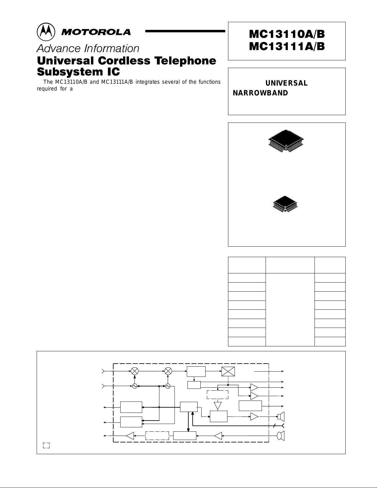
The MC13110A/B and MC13111A/B integrates several of the functions
required for a cordless telephone into a single integrated circuit. This
significantly reduces component count, board space requirements, external
adjustments, and lowers overall costs. It is designed for use in both the
handset and the base.
• MC13110A and MC13111A: Fully Programmable in all Power Modes
• MC13110B and MC13111B: MPU Clk Out and Second Local Oscillator
are “Always On”. There is No Inactive Mode
• Dual Conversion FM Receiver
– Complete Dual Conversion Receiver – Antenna Input to Audio Out
80 MHz Maximum Carrier Frequency
– RSSI Output
– Carrier Detect Output with Programmable Threshold
– Comparator for Data Recovery
– Operates with Either a Quad Coil or Ceramic Discriminator
• Compander
– Expander Includes Mute, Digital Volume Control, Speaker Driver,
Programmable Low Pass Filter, and Gain Block
– Compressor Includes Mute, Programmable Low Pass Filter, Limiter,
and Gain Block
• MC13110A/B only: Frequency Inversion Scrambler
– Function Controlled via MPU Interface
– Programmable Carrier Modulation Frequency
• Dual Universal Programmable PLL
– Supports New 25 Channel U.S. Standard with No External Switches
– Universal Design for Domestic and Foreign Cordless Telephone
Standards
– Digitally Controlled V ia a Serial Interface Port
– Receive Side Includes 1st LO VCO, Phase Detector, and 14–Bit
Programmable Counter and 2nd LO with 12–Bit Counter
– Transmit Section Contains Phase Detector and 14–Bit Counter
– MPU Clock Outputs Eliminates Need for MPU Crystal
• Low Battery Detect
– Provides Two Levels of Monitoring with Separate Outputs
– Separate, Adjustable Trip Points
• 2.7 to 5.5 V Operation (15 µA Current Consumption in Inactive Mode)
• AN1575: Refer to this Application Note for a List of the “Worldwide
Cordless Telephone Frequencies
Simplified Block Diagram
UNIVERSAL
NARROWBAND FM RECEIVER
INTEGRATED CIRCUIT
52
1
FB SUFFIX
PLASTIC PACKAGE
CASE 848B
(QFP–52)
48 1
FTA SUFFIX
PLASTIC PACKAGE
CASE 932
(LQFP–48)
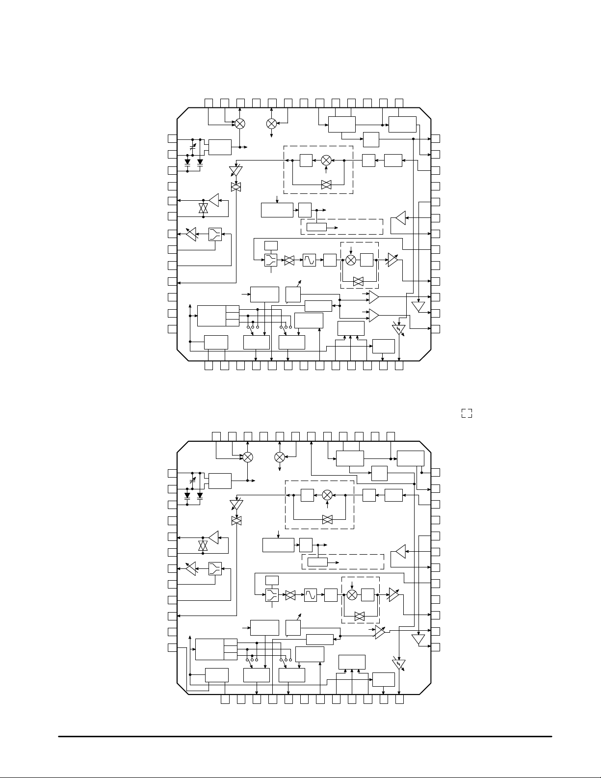
ORDERING INFORMATION
Tested Operating
Device
MC13110AFB
MC131 10AFTA
MC131 10BFB QFP–52
MC131 10BFTA LQFP–48
MC13111AFB
MC13111AFTA
MC13111BFB
MC13111BFTA
Temperature Range
TA = – 40° to +85°C
Package
QFP–52
LQFP–48
QFP–52
LQFP–48
QFP–52
LQFP–48
Rx In
Rx PD In
Rx PD Out
Tx PD Out
NOTE:
= MC13110A/B Only
This document contains information on a new product. Specifications and information herein
are subject to change without notice.
MOTOROLA ANALOG IC DEVICE DATA
Tx Out
1st
Mixer
1st LO 2nd LO
Rx Phase
Detector
Tx Phase
Detector
Scrambler
This device contains 8262 active transistors.
Limiting IF
2nd
Mixer
µ
P Serial
Interface
Compressor
Amplifier
RSSI
Scrambler
Expander
2nd LO
Detector
Low Battery
Detect
Motorola, Inc. 1997 Rev 0
MPU Clock Out
RSSI
Carrier Detect Out
Data Out
Low Battery
Indicator
Rx Out
SPI
Tx In
1
Page 2
MC13110A/B MC13111A/B
PIN CONNECTIONS
QFP–52
2
In
Mix
39
1
1
In
1
Mix
38
Out
Mix
37
1
Gnd RF
36
Out
Mix
35
In
2
2
Mix
34
Lim In
SGnd RF
32
33
Lim C1
31
Lim C2
30
RF
CC
V
29
Lim Out
28
Q Coil
27
In
LO
1
Out
LO
1
Ctrl
V
cap
Gnd Audio
SA Out
SA In
E Out
E
cap
E In
Scr Out
Ref
2
Ref
1
VB
40
41
42
43
44
45
46
47
48
49
50
51
52
Speaker
Mute
Vol
Control
2nd LO
1st Mix 2nd Mix
1st LO
VCO
1st LO
Rx Gain
Adjust
In
Mix
36
1
1
1st LO
÷
25
÷
4
÷
1
2
Out
2
LO
35
R
x
Mute
Compressor
Rx Phase
Detect
3
Vag
2
In
1
Mix
34
Speaker
Amp
Expander
12 b Prog
Ref Ctr
2nd LO
10.240
1
InLO
2
2nd LO
14 b Prog
Rx Ctr
4
PD
x
R
Out
1
Mix
2nd LO
6 b Prog
SC Clk Ctr
ALC
Mute
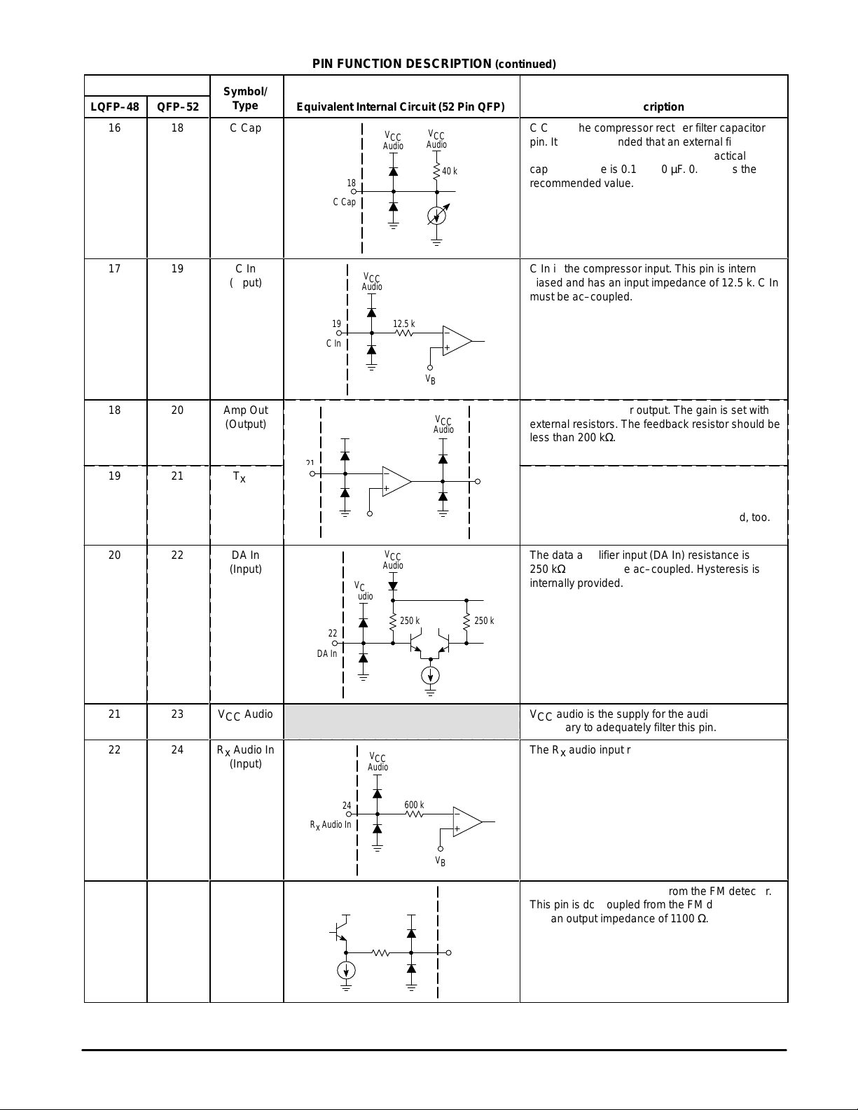
C Cap
Tx Phase
5
ref
PLL V
Out
2
Gnd RF
Mix
32
33
Scrambler
LPF
4.129 kHz
Bypass
÷
2
T
x
Limiter
VB
V
ref
Reg 2.5 V
14 b Prog
Tx Ctr
Detect
7
6
PD
x
T
Gnd PLL
LQFP–48
In
2
Mix
31
÷
40
RSSI
30
IF Amp/
Limiter
SC Filter
Clock
Scrambler
Modulating Clock
LPF
µ
9
8
Data
VCO
x
T
Lim In
29
4.129 kHz
Bypass
Ref
Ref
P Serial
Interface
10
EN
Lim C1
28
RSSI
LPF AALPF
Mic Amp
LPF
2
Low Battery
Detect
1
Prog
Clk Ctr
11
Clk
RF
CC
V
Lim C2
26
27
Detector
Tx Gain
Adjust
12
Clk Out
Lim Out
25
Data
Amp
Carrier
Detect
13
CD Out
26
25
24
23
22
21
20
19
18
17
16
15
14
RSSI
Det Out
R
Audio In
x
V
Audio
CC
DA In
T
In
x
Amp Out
C In
C Cap
T
Out
x
BD2 Out
DA Out
BD1 Out
NOTE:
= MC13110A/B Only
LO
In
1
LO
Out
1
Ctrl
V
cap
Gnd Audio
SA Out
SA In
E Out
E
cap
E In
Scr Out
VB
LO
In
2
37
38
39
40
41
42
43
44
45
46
47
48
Speaker
Mute
Vol
Control
2nd LO
1st LO
VCO
Speaker
Amp
Expander
12 b Prog
Ref Ctr
2nd LO
10.240
1st Mix 2nd Mix
2nd LO
1st LO
Rx Gain
Adjust
R
x
Mute
2nd LO
6 b Prog
SC Clk Ctr
T
ALC
Mute
Compressor
C Cap
÷
1
OutLO
14 b Prog
Rx Ctr
25
÷
4
÷
1
Rx Phase
Detect
2
Vag
2
Tx Phase
Detect
4
3
ref
PD
x
R
PLL V
1st LO
Scrambler
LPF
4.129 kHz
Bypass
÷
2
x
Limiter
VB
V
ref
14 b Prog
Tx Ctr
6
5
PD
x
T
Gnd PLL
÷
40
LPF
Reg 2.5 V
7
VCO
x
T
IF Amp/
Limiter
SC Filter
Clock
Scrambler
Modulating Clock
4.129 kHz
Bypass
VCC Audio
µ
P Serial
Interface
9
8
EN
Data
RSSI
LPF AALPF
Mic Amp
Tx Gain
Adjust
LPF
Programmable
Low Battery
Detect
Prog
Clk Ctr
11
10
Clk
Clk Out
Detector
Data
Amp
Carrier
Detect
12
CD Out
24
23
22
21
20
19
18
17
16
15
14
13
Q Coil
Det Out
R
Audio In
x
V
Audio
CC
DA In
T
In
x
Amp Out
C In
C Cap
T
Out
x
BD Out
DA Out
2
MOTOROLA ANALOG IC DEVICE DATA
Page 3
MC13110A/B MC13111A/B
БББББ
БББББ
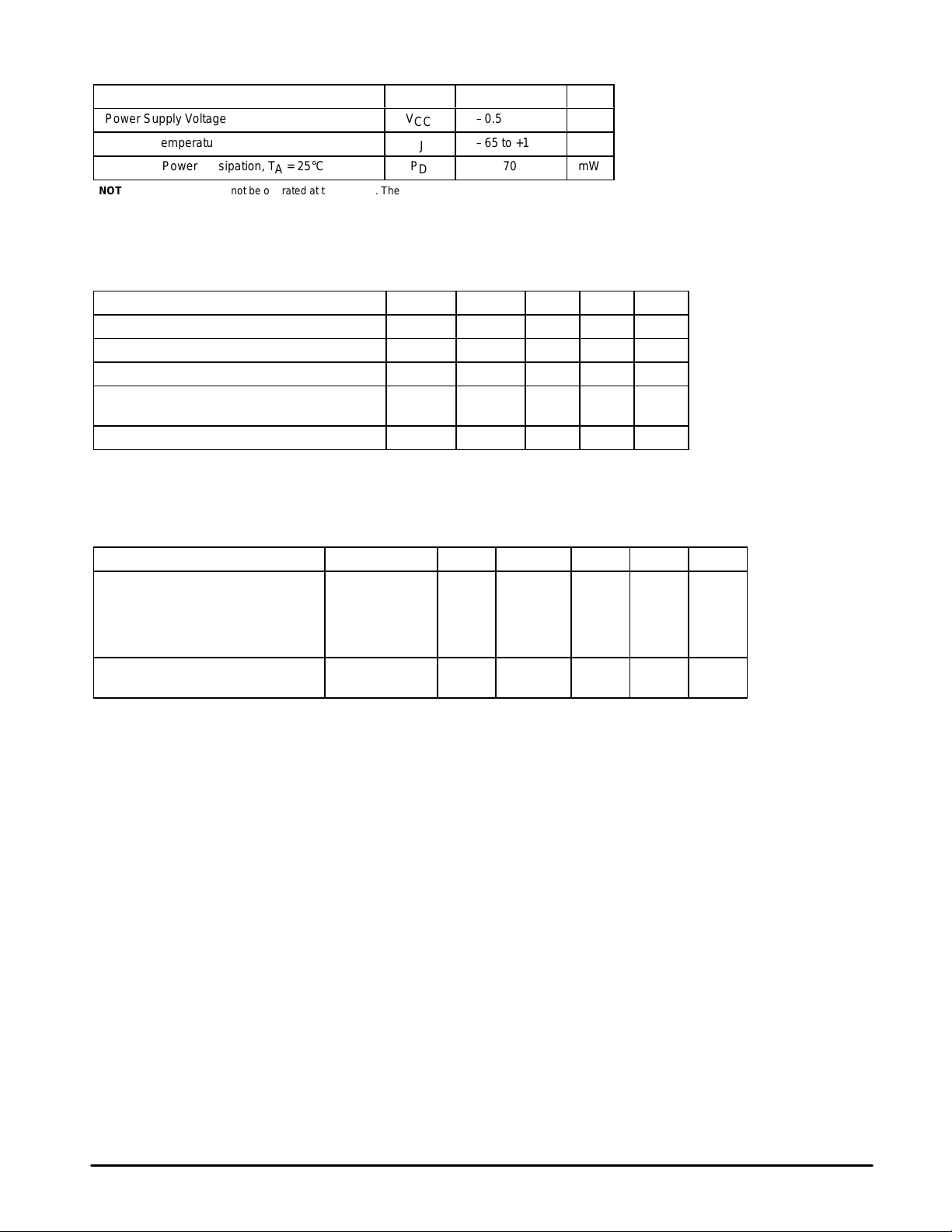
MAXIMUM RATINGS
Characteristic Symbol Value Unit
Power Supply Voltage
Junction Temperature
Maximum Power Dissipation, TA = 25°C P
NOTES: 1. Devices should not be operated at these limits. The “Recommended Operating Conditions”
provide for actual device operation.
2.ESD data available upon request.
RECOMMENDED OPERATING CONDITIONS
Characteristic Symbol Min Typ Max Unit
Supply Voltage V
Operating Ambient Temperature T
Input Voltage Low (Data, Clk, EN) V
Input Voltage High (Data, Clk, EN) V
Bandgap Reference Voltage V
NOTE: 3.All limits are not necessarily functional concurrently.
V
CC
T
J
D
CC
A
IL
IH
B
–0.5 to +6.0
–65 to +150
70 mW
2.7 3.6 5.5 Vdc
–40 – 85 °C
– – 0.3 V
PLL V
0.3
ref
–
– – V
– 1.5 – V
Vdc
°C
DC ELECTRICAL CHARACTERISTICS (V
= 3.6 V, TA = 25°C, unless otherwise specified, IP3 = 0;
CC
Test Circuit Figure 1.)
Characteristic
Symbol Figure Min Typ Max Unit
Static Current 1
Active Mode ACT I
Receive Mode Rx I
Standby Mode STD I
Inactive Mode [Note 4] INACT I
Current Increase When IP3 = 1
(Active and Receive Modes)
NOTE: 4.MC13110B/MC13111B versions have no inactive mode.
I
CC
CC
CC
CC
IP3
5.5 8.5 10.5 mA
3.1 4.1 5.3 mA
– 465 560 µA
– 15 30 µA
1 – 1.4 1.8 mA
MOTOROLA ANALOG IC DEVICE DATA
3
Page 4
MC13110A/B MC13111A/B
ELECTRICAL CHARACTERISTICS (V
Test Circuit Figure 1.)
Characteristic
FM RECEIVER (fRF = 46.77 MHz [USA Ch 21], f
Input Sensitivity (for 12 dB SINAD at Det Out
Using C–Message Weighting Filter)
50 Ω T ermination, Generator Referred
Single–Ended, Matched Input, Generator
Referred
Differential, Matched Input, Generator Referred –
First and Second Mixer Voltage Gain Total
(Vin = 1.0 mVrms, with CF1 and CF2 Load)
Isolation of First Mixer Output and Second Mixer
Input (Vin = 1.0 mVrms, with CFI Removed)
Total Harmonic Distortion (Vin = 3.16 mVrms) 1 Mix
Recovered Audio (Vin = 3.16 mVrms) 1 Mix
AM Rejection Ratio (Vin = 3.16 mVrms, 30% AM,
@ 1.0 kHz)
Signal to Noise Ratio (Vin = 3.16 mVrms,
No Modulation)
FIRST MIXER (No Modulation, fin = USA Ch21, 46.77 MHz, 50 Ω T ermination at Inputs)
Input Impedance
Single–Ended
Differential 16 Mix
Output Impedance 14 – Mix1 Out RP1 Out
Voltage Conversion Gain
(Vin = 1.0 mVrms, with CF1 Filter as Load)
1.0 dB Voltage Compression Level (Input Referred)
IP3 Bit Set to 0
IP3 Bit Set to 1 20, 21 –
Third Order Intercept (Input Referred) [Note 5]
IP3 Bit Set to 0
IP3 Bit Set to 1 20, 21 –
–3.0 dB IF Bandwidth 22 Mix1 In
NOTE: 5.Third order intercept calculated for input levels 10 dB below 1.0 dB compression point.
= 3.6 V, VB = 1.5 V, TA = 25°C, Active or Rx Mode, unless otherwise specified;
CC
Figure
= ±3.0 kHz, f
dev
68, 69 Mix
1 Mix
– Mix
1 Mix
– Mix
16
17, 18 Mix
19, 21
19, 21
Input
Pin
mod
In1/In
In1 or In
In1 or In
In1 or In
In1 or In
In1 or In
In1 or In
–
In1 or In
Mix
In1 or In
Mix
In1 or In
or In
Measure
Pin
= 1.0 kHz, V
1
1
1
1
1
1
1
1
1
1
Det Out V
2
Mix2 Out MX
2
Mix2 In Mix–Iso – 60 – dB
2
Det Out THD – 1.4 2.0 %
2
Det Out AFO 80 112 150 mVrms
2
Det Out AMR 30 48 – dB
2
Det Out SNR – 48 – dB
2
Mix
In1 or In
In1/In
Mix1 Out MX
2
Mix1 Out VO Mix
2
Mix1 Out TOI
2
Mix1 Out Mix1 BW – 13 – MHz
1
2
Symbol Min Typ Max Unit
= 1.2 V)
cap ctrl
SIN
gainT
1
R
2
PS1
C
PS1
1
R
2
PD1
C
PD1
CP1 Out
gain1
1 dB
mix1
1
µVrms
–
–
–
–
–
24 29 – dB
–
–
–
–
–
–
– 12 – dB
–
–
–
–
–
–
2.2
–100
0.4
–115
0.4
–115
1.6
3.7
1.6
1.8
300
3.7
20
–21
56
–12
64
–11
178
–2.0
dBm
–
–
–
–
–
–
kΩ
–
–
–
–
–
–
–
–
–
–
–
–
–
–
pF
pF
mVrms
dBm
mVrms
dBm
Ω
4
MOTOROLA ANALOG IC DEVICE DATA
Page 5
MC13110A/B MC13111A/B
ELECTRICAL CHARACTERISTICS (continued) (V
Test Circuit Figure 1.)
Characteristic UnitMaxTypMinSymbol
SECOND MIXER (No Modulation, fin = 10.7 MHz, 50 Ω T ermination at Inputs)
Input Impedance 24 Mix2 In Mix2 In RP2 In
Output Impedance 24 – Mix2 Out RP2 Out
Voltage Conversion Gain
(Vin = 1.0 mVrms, with CF2 Filter as Load)
1.0 dB Voltage Compression Level (Input Referred)
IP3 Bit Set 0
IP3 Bit Set 1 29, 30 –
Third Order Intercept (Input Referred) [Note 6]
IP3 Bit Set 0
IP3 Bit Set 1 29, 30 –
–3.0 dB IF Bandwidth 31 Mix2 In Mix2 Out Mix2 BW – 2.5 – MHz
LIMITER/DEMODULA TOR (fin = 455 kHz, f
Input Impedance 49 Lim In Lim In R
Detector Output Impedance – – Det Out R
IF –ā3.0 dB Limiting Sensitivity
Demodulator Bandwidth – Lim In Det Out BW – 20 – kHz
RSSI/CARRIER DETECT (No Modulation)
RSSI Output Dynamic Range 56 Mix1 In RSSI RSSI – 80 – dB
DC Voltage Range 56 Mix1 In RSSI DC RSSI – 0.2 to
Carrier Detect Threshold
CD Threshold Adjust = (10100)
(Threshold Relative to Mix1 In Level)
Hysteresis, CD = (10100)
(Threshold Relative to Mix1 In Level)
Output High Voltage
CD = (00000), RSSI = 0.2 V
Output Low Voltage
CD = (11111), RSSI = 0.9 V
Carrier Detect Threshold Adjustment Range
(Programmable through MPU Interface)
Carrier Detect Threshold – Number of
Programmable Levels
NOTE: 6.Third order intercept calculated for input levels 10 dB below 1.0 dB compression point.
= ±3.0 kHz, f
dev
= 3.6 V, VB = 1.5 V, TA = 25°C, Active or Rx Mode, unless otherwise specified;
CC
Input
Figure
26, 27 Mix2 In Mix2 Out MX
28, 30
28, 30
1 Lim In Det Out IF Sens – 71 100 µVrms
57 Mix1 In CD Out V
57 Mix1 In CD Out Hys – 2.0 – dB
1 RSSI CD Out V
1 RSSI CD Out V
126 – – V
126 – – V
Pin
Mix2 In Mix2 Out V
Mix2 In Mix2 Out TOI
= 1.0 kHz)
mod
Measure
Pin
CP2 In
CP2 Out
gain2
O
Mix
2
1 dB
mix2
PLim
C
PLim
O
T
OH
OL
T
Range
Tn
–
–
–
–
– 20 – dB
–
–
–
–
–
–
–
–
– 1.1 – kΩ
– 15 – µVrms
VCC –
0.1
– 0.02 0.4 V
– –20 to
– 32 – –
2.8
3.6
1.5
6.1
32
–17
45
–14
136
–4.3
158
–3.0
1.5
16
1.5
3.6 – V
11
–
–
–
–
–
–
–
–
–
–
–
–
–
–
– Vdc
– dB
kΩ
pF
kΩ
pF
mVrms
dBm
mVrms
dBm
kΩ
pF
MOTOROLA ANALOG IC DEVICE DATA
5
Page 6
MC13110A/B MC13111A/B
pp
x
in
ELECTRICAL CHARACTERISTICS
Test Circuit Figure 1.)
Characteristic UnitMaxTypMinSymbol
Rx AUDIO PATH (fin = 1.0 kHz, Active Mode, scrambler bypassed)
Absolute Gain (Vin = –20 dBV) 1, 72 Rx Audio In SA Out G –4.0 0 4.0 dB
Gain Tracking
(Referenced to E Out for Vin = –20 dBV)
Vin = –30 dBV –21 –20 –19
Vin = –40 dBV –42 –40 –38
Total Harmonic Distortion (Vin = –20 dBV) 1, 76 Rx Audio In SA Out THD – 0.7 1.0 %
Maximum Input Voltage (VCC = 2.7 V) 76 Rx Audio In – – – –11.5 – dBV
Maximum Output Voltage (Increase input voltage
until output voltage THD = 5.0%, then measure
output voltage)
Input Impedance – Rx Audio In
Attack Time
E
= 0.5 µF, R
cap
Release Time
E
= 0.5 µF, R
cap
Compressor to Expander Crosstalk
Vin = –10 dBV, V(E
Rx Muting (∆ Gain)
Vin = –20 dBV, Rx Gain Adj = (01111)
Rx High Frequency Corner
Rx Path, V Rx Audio In = –20 dBV
Low Pass Filter Passband Ripple (Vin = –20 dBV) 1, 73 Rx Audio In Scr Out Ripple – 0.4 0.6 dB
Rx Gain Adjust Range (Programmable through
MPU Interface)
Rx Gain Adjust Steps – Number of
Programmable Levels
Audio Path Noise, C–Message Weighting
(Input AC–Grounded)
Volume Control Adjust Range 123 E In E Out Vcn
Volume Control – Number of Programmable
Levels
SPEAKER AMP/SP MUTE (Active Mode)
Maximum Output Swing
RL = No Load, Vin = 3.4 Vpp
RL = 130 Ω, Vin = 2.8 Vpp
RL = 620 Ω, Vin = 4.0 Vpp
Speaker Amp Muting
Vin = –20 dBV, RL = 130 Ω
= 40 k (See Appendix B)
filt
= 40 k (See Appendix B)
filt
= AC Gnd
In)
(continued) (VCC = 3.6 V, VB = 1.5 V, TA = 25°C, Active or Rx Mode, unless otherwise specified;
Input
Figure
1, 76 E In E Out G
1 E In E Out V
– E In E Out t
– E In E Out t
1 C In E Out C
1 Rx Audio In E Out M
1 Rx Audio In Scr Out Rx f
125 Rx Audio In Scr Out R
125 Rx Audio In Scr Out Rx n – 20 – dB
70 Rx Audio In Scr Out
123 E In E Out V
1, 79 SA In SA Out V
1 SA In SA Out M
Pin
E In
Measure
Pin
– Z
E Out
SA Out
t
Omax
in
a
r
T
e
ch
x
Range
EN –
Range
cn
Omax
sp
dB
–2.0 0 – dBV
– 600
– 7.5 –
– 3.0 – ms
– 13.5 – ms
– –90 –70 dB
– –84 –60 dB
3.779 3.879 3.979 kHz
– –9.0 to
–
– –14 to
– 16 – –
2.8
2.0
–
– –92 –60 dB
10
–85
<–95
<–95
16
3.2
2.6
3.4
– k Ω
– dB
–
dBV
–
– dB
–
–
–
Vpp
6
MOTOROLA ANALOG IC DEVICE DATA
Page 7
MC13110A/B MC13111A/B
x
p
ELECTRICAL CHARACTERISTICS (continued) (V
Test Circuit Figure 1.)
Characteristic UnitMaxTypMinSymbol
DATA AMP COMPARATOR
Hysteresis 1 DA In DA Out Hys 30 42 50 mV
Threshold Voltage – DA In DA Out V
Input Impedance 1 – DA In Z
Output Impedance – – DA Out Z
Output High Voltage
Vin = VCC – 1.0 V, IOH = 0 mA
Output Low Voltage
Vin = VCC – 0.4 V, IOL = 0 mA
Maximum Frequency – DA In DA Out F
MIC AMP (fin = 1.0 kHz, External resistors set to gain of 1, Active Mode)
Open Loop Gain – Tx In Amp Out AVOL – 100,000 – V/V
Gain Bandwidth – Tx In Amp Out GBW – 100 – kHz
Maximum Output Swing (RL = 10 kΩ) – Tx In Amp Out V
Tx AUDIO PATH (fin = 1.0 kHz, Tx Gain Adj = (01111); ALC, Limiter, and Mutes Disabled; Active Mode, scrambler bypassed)
Absolute Gain (Vin = –10 dB V) 1, 83 Tx In Tx Out G –4.0 0 4.0 dB
Gain Tracking
(Referenced to Tx Out for Vin = –10 dBV)
Vin = –30 dBV
Vin = –40 dBV
Total Harmonic Distortion (Vin = –10 dBV) 1, 87 Tx In Tx Out THD – 0.8 1.8 %
Maximum Output Voltage (Increase input voltage
until output voltage THD = 5.0%, then measure
output voltage. Tx Gain Adjust = 8 dB)
Input Impedance – – C In Z
Attack Time (C
Appendix B))
Release Time (C
Appendix B))
Expander to Compressor Crosstalk (Vin = –20 dBV,
Speaker Amp No Load, V(C
Tx Muting (Vin – 10 dBV) 1 Tx In Tx Out M
ALC Output Level (ALC enabled)
Vin = –10 dBV
Vin = –2.5 dBV
ALC Slope (ALC enabled)
Vin = –10 dBv
Vin = –2.5 dBv
ALC Input Dynamic Range – C In Tx Out DR – –16 to
Limiter Output Level (Vin = –2.5 dBV,
Limiter enabled)
Tx High Frequency Corner [Note 7]
(VTx In = –10 dBV, Mic Amp = Unity Gain)
NOTE: 7.The filter specification is based on a 10.24 MHz 2nd LO, and a switched–capacitor (SC) filter counter divider ratio of 31. If other 2nd LO frequencies
= 0.5 µF, R
cap
= 0.5 µF, R
cap
and/or SC filter counter divider ratios are used, the filter corner frequency will be proportional to the resulting SC filter clock frequency.
= 40 k (See
filt
= 40 k (See
filt
= AC Gnd)
In)
= 3.6 V, VB = 1.5 V, TA = 25°C, Active or Rx Mode, unless otherwise specified;
CC
Input
Figure
1 DA In DA Out V
1 DA In DA Out V
1, 87 Tx In Tx Out G
1 Tx In Tx Out V
– C In Tx Out t
– C In Tx Out t
1 E In Tx Out C
1, 87,
90
1 Tx In
1 Tx In Tx Out V
1 Tx In Tx Out Tx f
Pin
Tx In Tx Out ALC
Measure
Pin
Tx Out
T
I
O
OH
OL
max
Omax
t
Omax
in
a
r
T
c
out
Slope
lim
– VCC –
200 250 280 kΩ
– 100 – kΩ
VCC –
0.1
– 0.1 0.4 V
– 10 – kHz
– 3.2 – Vpp
–11
–17
–2.0 0 – dBV
– 10 – kΩ
– 3.0 – ms
– 13.5 – ms
– –60 –40 dB
– –88 –60 dB
–15
–13
0.1 0.25 0.4 dB/dB
–10 –8.0 – dBV
3.6 3.7 3.8 kHz
c
0.7
3.6 – V
–10
–15
–13
–11
–2.5
– V
dB
–9.0
–13
dBV
–8.0
–6.0
– dBV
MOTOROLA ANALOG IC DEVICE DATA
7
Page 8
MC13110A/B MC13111A/B
x
,
in
ELECTRICAL CHARACTERISTICS
Test Circuit Figure 1.)
Characteristic UnitMaxTypMinSymbol
Tx AUDIO PATH (fin = 1.0 kHz, Tx Gain Adj = (01111); ALC, Limiter, and Mutes Disabled; Active Mode, scrambler bypassed)
Low Pass Filter Passband Ripple (Vin = –10 dBV) 1, 84 Tx In Tx Out Ripple – 0.7 1.2 dB
Maximum Compressor Gain (Vin = –70 dBV) – C In Tx Out AV
Tx Gain Adjust Range (Programmable through
MPU Interface)
Tx Gain Adjust Steps – Number of Programmable
Levels
Rx AND Tx SCRAMBLER (2nd LO = 10.24 MHz, Tx Gain Adj = (01111), Rx Gain Adj = (01111), Volume Control = (0 dB Default Levels),
SCF Clock Divider = 31. Total is divide by 62 for SCF clock frequency of 165.16 kHz)
Rx High Frequency Corner (Note 8)
Rx Path, f = 479 Hz, V Rx Audio In = –20 dBV
Tx High Frequency Corner (Note 8)
Tx Path, f = 300 Hz, V Tx In = –10 dBV,
Mic Amp = Unity Gain
Absolute Gain
Rx: Vin = –20 dBV
Tx: Vin = –10 dBV, Limiter disabled
Pass Band Ripple
Rx + Tx Path – 1.0 µF from Tx Out to
Rx Audio In, fin = low corner frequency to
high corner frequency
Scrambler Modulation Frequency
Rx: 100 mV (–20 dBV)
Tx: 316 mV (–10 dBV)
Group Delay
Rx + Tx Path – 1.0 µF from Tx Out to
Rx Audio In, fin = 1.0 kHz
fin = low corner frequency to high corner
frequency
Carrier Breakthrough
Rx + Tx Path – 1.0 µF from Tx Out to
Rx Audio In
Baseband Breakthrough
Rx + Tx Path – 1.0 µF from Tx Out to
Rx Audio In,
fin = 1.0 kHz, f
LOW BATTERY DETECT
Average Threshold
Voltage Before Electronic Adjustment
(V
_Adj = (0111))
ref
Average Threshold
Voltage After Electronic Adjustment
(V
_Adj = (adjusted value))
ref
Hysteresis – Ref
Input Current (Vin = 1.0 and 2.0 V) 1 – Ref
Output High Voltage (Vin = 2.0 V) 1 Ref
NOTE: 8.The filter specification is based on a 10.24 MHz 2nd LO, and a switch–capacitor (SC) filter counter divider ratio of 31. If other 2nd LO frequencies
and/or SC filter counter divider ratios are used, the filter corner frequency will be proportional to the resulting SC filter clock frequency.
meas
= 3.192 kHz
(continued) (VCC = 3.6 V, VB = 1.5 V, TA = 25°C, Active or Rx Mode, unless otherwise specified;
Input
Figure
125 C In Tx Out Tx Range – –9.0 to
125 C In Tx Out Tx n – 20 – –
– Rx Audio In Scr Out Rx f
– Tx In Tx Out Tx f
–
–
– C In E Out Ripple – 1.9 2.5 dB
–
–
– C In E Out GD – 1.0 –
– C In E Out GD – 4.0 –
– C In E Out CBT – –60 – dB
– C In E Out BBT – –50 – dB
1, 131 Ref
1 Ref
Pin
Rx Audio In
Tx In
Rx Audio In
C In
Ref
Ref
Ref
Ref
Measure
Pin
max
ch
ch
E Out
Tx Out
E Out
Tx Out
BD1 Out
1
BD2 Out
2
BD1 Out
1
BD2 Out
2
BD1 Out
1
BD2 Out
2
1
Ref
2
BD1 Out
1
BD2 Out
2
AV
f
mod
VT
i
VT
f
Hys – 4.0 – mV
I
in
V
OH
– 23 – dB
10
3.55 3.65 3.75 kHz
3.829 3.879 3.929 kHz
–4.0
–4.0
4.119 4.129 4.139 kHz
1.38 1.48 1.58 V
1.475 1.5 1.525 V
–50 – 50 nA
VCC –
0.1
0.4
–1.0
3.6 – V
– dB
dB
4.0
4.0
ms
8
MOTOROLA ANALOG IC DEVICE DATA
Page 9
MC13110A/B MC13111A/B
CC
ELECTRICAL CHARACTERISTICS (continued) (V
Test Circuit Figure 1.)
Characteristic UnitMaxTypMinSymbol
LOW BATTERY DETECT
Output Low Voltage (Vin = 1.0 V) 1 Ref
BATTERY DETECT INTERNAL THRESHOLD
After Electronic Adjustment of VB Voltage
BD Select = (111)
BD Select = (110) IBS
BD Select = (101) IBS
BD Select = (100) IBS
BD Select = (011) IBS
BD Select = (010) IBS
BD Select = (001) IBS
PLL PHASE DETECTOR
Output Source Current
(VPD = Gnd + 0.5 V to PLL V
Output Sink Current
(VPD = Gnd + 0.5 V to PLL V
PLL LOOP CHARACTERISTICS
Maximum 2nd LO Frequency
(No Crystal)
Maximum 2nd LO Frequency
(With Crystal)
Maximum Tx VCO (Input Frequency),
Vin = 200 mVpp
PLL VOLTAGE REGULATOR
Regulated Output Level (IL = 0 mA, after V
Adjustment)
Line Regulation (IL = 0 mA, VCC = 3.0 to 5.5 V) 1 VCC Audio PLL V
Load Regulation (IL = 1.0 mA) 1 VCC Audio PLL V
MICROPROCESSOR SERIAL INTERFACE
Input Current Low (Vin = 0.3 V, Standby Mode) 1 – Data,
Input Current High (Vin = 3.3 V, Standby Mode) 1 – Data,
Hysteresis Voltage – – Data,
Maximum Clock Frequency – Data,
Input Capacitance – Data,
EN to Clk Setup Time 106 – EN, Clk t
Data to Clk Setup Time 105 – Data, Clk t
Hold Time 105 – Data, Clk t
Recovery Time 106 – EN, Clk t
Input Pulse Width – – EN, Clk t
MPU Interface Power–Up Delay (90% of PLL V
to Data,Clk, EN)
– 0.5 V)
ref
– 0.5 V)
ref
ref
ref
= 3.6 V, VB = 1.5 V, TA = 25°C, Active or Rx Mode, unless otherwise specified;
CC
Input
Figure
1, 128 VCC Audio
– – Rx PD
– – Rx PD
– LO2 In – f
– – LO2 In
– – Tx VCO f
1 – PLL V
108 – – t
Pin
Ref
EN, Clk
Clk, EN
Measure
Pin
BD1 Out
1
BD2 Out
2
BD2 Out V
Tx PD
Tx PD
LO2 Out
txmax
ref
refVReg
V
ref
Clk, EN
Clk, EN
Clk, EN
– – – 2.0 – MHz
– C
V
suDC
puMPU
V
OL
IBS
7
6
5
4
3
2
1
I
OH
I
OL
2ext
f
2ext
V
O
Line – 11.8 40 mV
Reg
Load
I
IL
I
IH
hys
in
suEC
h
rec
w
– 0.2 0.4 V
3.381 3.455 3.529
3.298 3.370 3.442
3.217 3.287 3.357
3.134 3.202 3.270
2.970 3.034 3.098
2.886 2.948 3.010
2.802 2.862 2.922
– 1.0 – mA
– 1.0 – mA
– 12 – MHz
– 12 – MHz
– 80 – MHz
2.4 2.5 2.6 V
–20 –1.4 – mV
–5.0 0.4 – µA
– 1.6 5.0 µA
– 1.0 – V
– 8.0 – pF
– 200 – ns
– 100 – ns
– 90 – ns
– 90 – ns
– 100 – ns
– 100 – µs
MOTOROLA ANALOG IC DEVICE DATA
9
Page 10
MC13110A/B MC13111A/B
2
L
22.1 k
CC
V
10
0.1
µ
10 F
0.1 0.1
2
CF
455 kHz
332
CC
To V
Figure 1. Production Test Circuit (52 Pin QFP)
1
CF
10.7 MHz
Audio In
x
R
1000
Det Out
15 k
0.01
0.1
27282930313233343536373839
Coil
Q
RF
2
1
2
In
Out
Out
1
In
1
Audio
CC
V
26
RSSI
Lim Out
CC
V
Lim C
Lim C
Lim In
SGnd RF
Mix
2
Mix
Gnd RF
1
Mix
1In2
Mix
Mix
1In1
LO
40
0.1
µ
10 F
25
Det Out
Out
LO
41
In
x
T
DA In
49.9 k
0.1
23
24
Audio
Audio In
CC
x
V
R
V Cap Ctrl
Gnd Audio
42
43
0.1
49.9 k
22
DA In
SA Out
44
Mic Amp Out
21
In
x
T
MC13110A/B
SA In
45
C In
0.1
20
C In
Amp Out
IC
MC13111A/B
E Out
E Cap
46
0.1
0.1
19
47
CCA
V
18
C Cap
E In
48
Out
x
T
F
µ
1.0
7.5 k
Out
2
Data Out
BD
CC
V
100 k
15
16
17
Out2Out1Out
x
T
DA Out
BD
BD
ref
2
1
Scr Out
Ref
Ref
V
51
50
49
µ
Out
1
BD
CC
V
Carrier
100 k
Detect Out
≥
Legend:
If 1, then capacitor value = pF
If <1, then capacitor value = F
100 k
14
Out
13121110987543216
CD
Clk Out
Clk
MPU Clock Output
VCO
x
T
0.1
µ
10 F
0.1
Out
In
B
VCO
PD
PD
2
2
EN
Data
x
T
Gnd PLL
x
T
PLL V
x
R
ag
V
LO
LO
0.01
52
NOTE: This schematic is only a partial representation of the actual production test circuit.
10
0.01
RF In
49.9 0.01
L3
33
110
µ
10 F
SA Out
49.9 k
0.1
SA In
49.9 k
CCA
V
0.1
0.1
E In
µ
7.5 k
1.0 F
E Out
µ
1.0 F
5.0 – 50 8.2
10.240 MHz
0.1
0.1
0.047
3.01 k
1.0 k
1.0 k
1.5 k22.1 k
ref1
V
Scr Out
ref2
V
32.4 k
0.1
Loop Filter
x
R
4700
MOTOROLA ANALOG IC DEVICE DATA
Page 11
Pin
Symbol/
Á
Á
Á
Á
Á
Á
Á
Á
Á
Á
Á
Á
Á
Á
Á
Á
Á
Á
Á
Á
Á
Á
Á
Á
Á
Á
Á
Á
Á
Á
Á
Á
Á
Á
Á
Á
Á
Á
Á
Á
Á
Á
Á
Á
Á
Á
Á
Á
Á
Á
Á
Á
Á
Á
Á
Á
Á
Á
Á
Á
Á
Á
Á
Á
Á
Á
Á
Á
Á
Á
Á
Á
p
Á
Á
Á
Á
Á
Á
Á
Á
narrow pulses with a frequency equal to the
Á
Á
Á
Á
Á
Á
Á
Á
Á
Á
Á
Á
Á
Á
Á
Á
Á
Á
Á
Á
Á
Á
Á
Á
Á
Á
Á
Á
Á
Á
Á
Á
Á
Á
Á
Á
Á
Á
Á
Á
Á
Á
Á
Á
Á
Á
Á
Á
Á
Á
Á
Á
Á
Á
Á
Á
Á
Á
Á
Á
Á
Á
Á
Á
Á
Á
Á
Á
Á
Á
Á
Á
Á
Á
Á
LQFP–48
48
ÁÁ
1
ÁÁ
ÁÁ
ÁÁ
ÁÁ
ÁÁ
ÁÁ
ÁÁ
ÁÁ
ÁÁ
2
ÁÁ
ÁÁ
ÁÁ
ÁÁ
ÁÁ
ÁÁ
3
ÁÁ
ÁÁ
5
ÁÁ
ÁÁ
ÁÁ
4
ÁÁ
ÁÁ
ÁÁ
ÁÁ
ÁÁ
ÁÁ
ÁÁ
ÁÁ6ÁÁ7ÁÁÁ
7
ÁÁ
ÁÁ
ÁÁ
ÁÁ
ÁÁ
ÁÁ
ÁÁ
ÁÁ
ÁÁ
MOTOROLA ANALOG IC DEVICE DATA
QFP–52
1
ÁÁ
2
ÁÁ
ÁÁ
ÁÁ
ÁÁ
ÁÁ
ÁÁ
ÁÁ
ÁÁ
ÁÁ
3
ÁÁ
ÁÁ
ÁÁ
ÁÁ
ÁÁ
ÁÁ
4
ÁÁ
ÁÁ
6
ÁÁ
ÁÁ
ÁÁ
5
ÁÁ
ÁÁ
ÁÁ
ÁÁ
ÁÁ
ÁÁ
ÁÁ
8
ÁÁ
ÁÁ
ÁÁ
ÁÁ
ÁÁ
ÁÁ
ÁÁ
ÁÁ
ÁÁ
S
mbol/
Type
LO2 In
ÁÁÁ
LO2 Out
ÁÁÁ
ÁÁÁ
ÁÁÁ
ÁÁÁ
ÁÁÁ
ÁÁÁ
ÁÁÁ
ÁÁÁ
ÁÁÁ
V
ag
ÁÁÁ
ÁÁÁ
ÁÁÁ
ÁÁÁ
ÁÁÁ
ÁÁÁ
Rx PD
(Output)
ÁÁÁ
ÁÁÁ
Tx PD
(Output)
ÁÁÁ
ÁÁÁ
ÁÁÁ
PLL V
ref
ÁÁÁ
ÁÁÁ
ÁÁÁ
ÁÁÁ
ÁÁÁ
ÁÁÁ
ÁÁÁ
Gnd PLL
Tx VCO
ÁÁÁ
(Input)
ÁÁÁ
ÁÁÁ
ÁÁÁ
ÁÁÁ
ÁÁÁ
ÁÁÁ
ÁÁÁ
ÁÁÁ
MC13110A/B MC13111A/B
PIN FUNCTION DESCRIPTION
Equivalent Internal Circuit (52 Pin QFP)
PLL
V
ref
PLL
V
ref
100
3
V
ag
4, 6
Rx PD,
Tx PD
PLL
V
ref
PLL
V
ref
2
LO2
Out
100
LO
1
2
In
V
Audio
CC
PLL
V
PLL
V
ref
ref
30 k
PLL
V
ref
15
1.0 k
132 k
V
CC
Audio
ББББББББББ
ББББББББББ
ББББББББББ
PLL V
8
ref
PLL
V
ref
5
ББББББББББ
ББББББББББ
ББББББББББ
ББББББББББ
ББББББББББ
ББББББББББ
ББББББББББ
ББББББББББ
ББББББББББ
ББББББББББ
TX VCO
ББББББББББ
ББББББББББ
ББББББББББ
Description
These pins form the PLL reference oscillator when
БББББББББББ
connected to an external parallel–resonant crystal
(10.24 MHz typical). The reference oscillator is
БББББББББББ
also the second Local Oscillator (LO2) for the RF
БББББББББББ
receiver. “LO2 In” may also serve as an input for
an externally generated reference signal which is
БББББББББББ
typically ac–coupled.
БББББББББББ
When the IC is set to the inactive mode, LO2 In is
БББББББББББ
internally pulled low to disable the oscillator. The
input capacitance to ground at each pin (LO2 In/
БББББББББББ
LO2 Out) is 3.0 pF.
БББББББББББ
БББББББББББ
БББББББББББ
Vag is the internal reference voltage for the
БББББББББББ
switched capacitor filter section. This pin must be
БББББББББББ
decoupled with a 0.1 µF capacitor.
БББББББББББ
БББББББББББ
БББББББББББ
БББББББББББ
This pin is a tri–state voltage output of the Rx and
Tx Phase Detector. It is either “high”, “low”, or “high
БББББББББББ
impedance,” depending on the phase difference of
the phase detector input signals. During lock, very
БББББББББББ
narrow
ulses with a frequency equal to the
reference frequency are present. This pin drives
the external Rx and Tx PLL loop filters. Rx and T
БББББББББББ
PD outputs can sink or source 1.0 mA.
БББББББББББ
БББББББББББ
PLL V
internal voltage regulator provides a stable power
supply voltage for the Rx and Tx PLL’s and can
also be used as a regulated supply voltage for
other IC’s. It can source up to 1.0 mA externally.
Proper supply filtering is a must on this pin. PLL
V
inactive modes (Note 1).
Ground pin for digital PLL section of IC.
Tx VCO is the transmit divide counter input which
is driven by an ac–coupled external transmit loop
VCO. The minimum signal level is 200 mVpp @
60.0 MHz. This pin also functions as the test mode
input for the counter tests.
is a PLL voltage regulator output pin. An
ref
БББББББББББ
БББББББББББ
БББББББББББ
БББББББББББ
is pulled up to VCC audio for the standby and
ref
БББББББББББ
БББББББББББ
БББББББББББ
БББББББББББ
БББББББББББ
БББББББББББ
БББББББББББ
БББББББББББ
БББББББББББ
БББББББББББ
БББББББББББ
БББББББББББ
БББББББББББ
11
x
Page 12
LQFP–48
Á
Á
Á
Á
Á
Á
Á
Á
Á
Á
Á
Á
Á
Á
Á
Á
Á
Á
Á
Á
Á
Á
Á
Á
Á
Á
Á
Á
Á
Á
Á
Á
Á
Á
Á
Á
Á
Á
Á
Á
Á
Á
Á
Á
Á
Á
Á
Á
Á
Á
Á
Á
Á
Á
Á
Á
Á
Á
Á
Á
Á
Á
Á
Á
Á
Á
Á
Á
Á
Á
Á
Á
Á
Á
Á
Á
Á
Á
Á
Á
Á
Á
Á
Á
Á
Á
Á
Á
Á
Á
Á
Á
Á
Á
Á
Á
Á
Á
Á
Á
Á
Á
Á
Á
Á
Á
Á
Á
Á
Á
Á
Á
Á
Á
Á
Á
Á
Á
Á
Á
Á
Á
Á
Á
Á
Á
Á
Á
14, 16
Á
Á
Á
Á
Á
Á
Á
Á
Á
Á
Á
Á
Á
Á
Á
Á
Á
Á
Á
Á
Á
Á
Á
Á
Á
Á
Á
Á
Á
Á
Á
Á
Á
Á
Á
Á
Á
Á
Á
Á
Á
Á
Á
Á
Á
Á
Á
Á
Á
Á
Á
Á
8
9
ÁÁ
10
ÁÁ
ÁÁ
ÁÁ
ÁÁ
ÁÁ
11
ÁÁ
ÁÁ
ÁÁ
ÁÁ
ÁÁ
ÁÁ
ÁÁ
ÁÁ
ÁÁ
ÁÁ
12
ÁÁ
ÁÁ
ÁÁ
ÁÁ
ÁÁ
ÁÁ
–
ÁÁ
ÁÁ
Pin
QFP–52
ÁÁ
ÁÁ
ÁÁ
ÁÁ
ÁÁ
ÁÁ
ÁÁ
ÁÁ
ÁÁ
ÁÁ
ÁÁ
ÁÁ
ÁÁ
ÁÁ
ÁÁ
ÁÁ
ÁÁ
ÁÁ
ÁÁ
ÁÁ
ÁÁ
ÁÁ
ÁÁ
ÁÁ
10
12
13
14
MC13110A/B MC13111A/B
PIN FUNCTION DESCRIPTION (continued)
Symbol/
Symbol/
Type
Type
9
11
Data
EN
ÁÁÁ
Clk
ÁÁÁ
(Input)
ÁÁÁ
ÁÁÁ
ÁÁÁ
ÁÁÁ
Clk Out
ÁÁÁ
(Output)
ÁÁÁ
ÁÁÁ
ÁÁÁ
ÁÁÁ
ÁÁÁ
ÁÁÁ
ÁÁÁ
ÁÁÁ
ÁÁÁ
CD Out
ÁÁÁ
(I/O)
ÁÁÁ
ÁÁÁ
ÁÁÁ
ÁÁÁ
ÁÁÁ
BD1 Out
ÁÁÁ
ÁÁÁ
Equivalent Internal Circuit (52 Pin QFP)
Equivalent Internal Circuit (52 Pin QFP)
V
CC
9, 10, 11
V
Audio
V
Audio
CC
Audio
CC
240
240
1.0 µA
1.0 k
V
CC
Audio
V
CC
Audio
CD
Comparator
ББББББББББ
ББББББББББ
ББББББББББ
Data, EN, Clk
ББББББББББ
ББББББББББ
ББББББББББ
ББББББББББ
ББББББББББ
ББББББББББ
ББББББББББ
ББББББББББ
ББББББББББ
ББББББББББ
ББББББББББ
ББББББББББ
ББББББББББ
ББББББББББ
ББББББББББ
ББББББББББ
13
CD Out
ББББББББББ
ББББББББББ
ББББББББББ
ББББББББББ
ББББББББББ
PLL
V
ref
PLL
V
12
Clk Out
ref
Hardware
Interrupt
Microprocessor serial interface input pins are for
programming various counters and control
БББББББББББ
functions. The switching thresholds are referenced
БББББББББББ
to PLL V
VCC. These pins have 1.0 µA internal pull–down
currents.
The microprocessor clock output is derived from
the 2nd LO crystal oscillator and a programmable
divider with divide ratios of 2 to 312.5. It can be
used to drive a microprocessor and thereby
reduce the number of crystals required in the
system design. The driver has an internal resistor
in series with the output which can be combined
with an external capacitor to form a low pass filter
to reduce radiated noise on the PCB. This output
also functions as the output for the counter test
modes.
1) For the MC13110A/B and MC13111A/B the Clk
Out can be disabled via the MPU interface.
2) For the MC13110B and MC13111B this output is
always active (on) (Note 2).
Dual function pin;
1) Carrier detect output (open collector with
external 100 kΩ pull–up resistor.
2) Hardware interrupt input which can be used to
“wake–up” from the Inactive Mode.
ref
БББББББББББ
БББББББББББ
БББББББББББ
БББББББББББ
БББББББББББ
БББББББББББ
БББББББББББ
БББББББББББ
БББББББББББ
БББББББББББ
БББББББББББ
БББББББББББ
БББББББББББ
БББББББББББ
БББББББББББ
БББББББББББ
БББББББББББ
БББББББББББ
БББББББББББ
БББББББББББ
Low battery detect output #1 is an open collector
with external pull–up resistor.
БББББББББББ
БББББББББББ
Description
Description
and Gnd PLL. The inputs operate up to
ÁÁ
ÁÁ
ÁÁ
ÁÁ
ÁÁ
ÁÁ
ÁÁ
ÁÁ
ÁÁ
ÁÁ
ÁÁ
ÁÁ
12
14
13
15
16
ÁÁ
ÁÁ
15
ÁÁ
ÁÁ
ÁÁ
ÁÁ
ÁÁ
17
ÁÁ
ÁÁ
ÁÁ
ÁÁ
ÁÁ
BD2 Out
(Output)
ÁÁÁ
ÁÁÁ
DA Out
(Output)
ÁÁÁ
ÁÁÁ
ÁÁÁ
ÁÁÁ
ÁÁÁ
Tx Out
(Output)
ÁÁÁ
ÁÁÁ
ÁÁÁ
ÁÁÁ
ÁÁÁ
V
CC
Audio
V
Audio
CC
BD1 Out
BD2 Out
15
DA Out
17
Tx Out
ББББББББББ
ББББББББББ
100 k
V
B
VCC
Audio
ББББББББББ
ББББББББББ
ББББББББББ
ББББББББББ
ББББББББББ
ББББББББББ
ББББББББББ
ББББББББББ
ББББББББББ
ББББББББББ
Low battery detect output #2 is an open collector
with external pull–up resistor.
БББББББББББ
БББББББББББ
Data amplifier output (open collector with internal
100 kΩ pull–up resistor).
БББББББББББ
БББББББББББ
БББББББББББ
БББББББББББ
БББББББББББ
Tx Out is the Tx path audio output. Internally this
pin has a low–pass filter circuitry with –3 dB
БББББББББББ
bandwidth of 4.0 kHz. Tx gain and mute are
БББББББББББ
programmable through the MPU interface. This pin
is sensitive to load capacitance.
БББББББББББ
БББББББББББ
БББББББББББ
MOTOROLA ANALOG IC DEVICE DATA
Page 13
LQFP–48
Á
Á
Á
Á
Á
Á
Á
Á
Á
Á
Á
Á
Á
Á
Á
Á
Á
Á
Á
Á
Á
Á
Á
Á
Á
Á
Á
Á
Á
Á
Á
Á
Á
Á
Á
Á
Á
Á
Á
Á
Á
Á
Á
Á
Á
Á
Á
Á
Á
Á
Á
Á
Á
Á
Á
Á
Á
Á
Á
Á
Á
Á
Á
Á
Á
Á
Á
Á
Á
Á
Á
Á
Á
Á
Á
Á
Á
Á
Á
Á
Á
Á
21
Á
Á
Á
Á
Á
Á
Á
Á
Á
Á
Á
Á
Á
Á
Á
Á
Á
Á
Á
Á
Á
Á
Á
Á
Á
Á
Á
Á
Á
Á
Á
Á
Á
Á
Á
Á
Á
Á
Á
Á
Á
Á
Á
Á
Á
Á
Á
Á
Á
Á
Á
Á
Á
Á
Á
Á
Á
Á
Á
Á
Á
Á
Á
Á
Á
Á
Á
Á
Á
Á
Á
Á
Á
Á
Á
Á
Á
Á
Á
Á
Á
Á
Á
Á
Á
Á
Á
16
ÁÁ
ÁÁ
ÁÁ
ÁÁ
ÁÁ
ÁÁ
17
ÁÁ
ÁÁ
ÁÁ
ÁÁ
ÁÁ
ÁÁ
Pin
QFP–52
ÁÁ
ÁÁ
ÁÁ
ÁÁ
ÁÁ
ÁÁ
ÁÁ
ÁÁ
ÁÁ
ÁÁ
ÁÁ
ÁÁ
18
19
Symbol/
Symbol/
Type
Type
C Cap
ÁÁÁ
ÁÁÁ
ÁÁÁ
ÁÁÁ
ÁÁÁ
ÁÁÁ
C In
ÁÁÁ
(Input)
ÁÁÁ
ÁÁÁ
ÁÁÁ
ÁÁÁ
ÁÁÁ
MC13110A/B MC13111A/B
PIN FUNCTION DESCRIPTION (continued)
Equivalent Internal Circuit (52 Pin QFP)
Equivalent Internal Circuit (52 Pin QFP)
CC
12.5 k
V
CC
Audio
V
B
40 k
V
ББББББББББ
ББББББББББ
ББББББББББ
C Cap
ББББББББББ
ББББББББББ
ББББББББББ
ББББББББББ
ББББББББББ
ББББББББББ
19
ББББББББББ
C In
ББББББББББ
ББББББББББ
Audio
18
V
CC
Audio
Description
Description
C Cap is the compressor rectifier filter capacitor
pin. It is recommended that an external filter
БББББББББББ
capacitor to VCC audio be used. A practical
БББББББББББ
capacitor range is 0.1 to 1.0 µF. 0.47 µF is the
recommended value.
БББББББББББ
БББББББББББ
БББББББББББ
БББББББББББ
C In is the compressor input. This pin is internally
БББББББББББ
biased and has an input impedance of 12.5 k. C In
БББББББББББ
must be ac–coupled.
БББББББББББ
БББББББББББ
БББББББББББ
БББББББББББ
18
ÁÁ
ÁÁ
19
ÁÁ
ÁÁ
ÁÁ
20
ÁÁ
ÁÁ
ÁÁ
ÁÁ
ÁÁ
ÁÁ
21
ÁÁ
22
ÁÁ
ÁÁ
ÁÁ
ÁÁ
ÁÁ
ÁÁ
23
ÁÁ
ÁÁ
ÁÁ
ÁÁ
ÁÁ
MOTOROLA ANALOG IC DEVICE DATA
20
ÁÁ
ÁÁ
21
ÁÁ
ÁÁ
ÁÁ
22
ÁÁ
ÁÁ
ÁÁ
ÁÁ
ÁÁ
ÁÁ
23
ÁÁ
24
ÁÁ
ÁÁ
ÁÁ
ÁÁ
ÁÁ
ÁÁ
25
ÁÁ
ÁÁ
ÁÁ
ÁÁ
ÁÁ
Amp Out
(Output)
ÁÁÁ
ÁÁÁ
Tx In
(Input)
ÁÁÁ
ÁÁÁ
ÁÁÁ
DA In
(Input)
ÁÁÁ
ÁÁÁ
ÁÁÁ
ÁÁÁ
ÁÁÁ
ÁÁÁ
VCC Audio
ÁÁÁ
Rx Audio In
(Input)
ÁÁÁ
ÁÁÁ
ÁÁÁ
ÁÁÁ
ÁÁÁ
ÁÁÁ
Det Out
ÁÁÁ
(Output)
ÁÁÁ
ÁÁÁ
ÁÁÁ
ÁÁÁ
V
CC
ББББББББББ
Audio
ББББББББББ
V
CC
Audio
20
Tx In
ББББББББББ
ББББББББББ
ББББББББББ
ББББББББББ
ББББББББББ
ББББББББББ
ББББББББББ
DA In
ББББББББББ
ББББББББББ
ББББББББББ
ББББББББББ
ББББББББББ
Rx Audio In
ББББББББББ
ББББББББББ
ББББББББББ
ББББББББББ
ББББББББББ
ББББББББББ
ББББББББББ
ББББББББББ
V
B
V
CC
Audio
V
CC
Audio
250 k 250 k
22
V
CC
Audio
24
V
CC
RF
600 k
V
CC
Audio
240
30 µA
V
B
25
Det Out
Amp Out
Microphone amplifier output. The gain is set with
external resistors. The feedback resistor should be
БББББББББББ
less than 200 kΩ.
БББББББББББ
Tx In is the Tx path input to the microphone
amplifier (Mic Amp). An external resistor is
БББББББББББ
connected to this pin to set the Mic Amp gain and
БББББББББББ
input impedance. Tx In must be ac–coupled, too.
БББББББББББ
The data amplifier input (DA In) resistance is
250 kΩ and must be ac–coupled. Hysteresis is
БББББББББББ
internally provided.
БББББББББББ
БББББББББББ
БББББББББББ
БББББББББББ
БББББББББББ
VCC audio is the supply for the audio section. It is
БББББББББББ
necessary to adequately filter this pin.
The Rx audio input resistance is 600 kΩ and must
be ac–coupled.
БББББББББББ
БББББББББББ
БББББББББББ
БББББББББББ
БББББББББББ
БББББББББББ
Det Out is the audio output from the FM detector.
БББББББББББ
This pin is dc–coupled from the FM detector and
has an output impedance of 1100 Ω.
БББББББББББ
БББББББББББ
БББББББББББ
БББББББББББ
13
Page 14
LQFP–48
Á
Á
Á
Á
Á
Á
Á
Á
Á
Á
Á
Á
Á
Á
Á
Á
Á
Á
Á
Á
Á
Á
Á
Á
Á
Á
Á
Á
Á
Á
Á
Á
Á
Á
Á
Á
Á
Á
Á
Á
Á
Á
Á
Á
Á
Á
Á
Á
Á
Á
Á
Á
Á
Á
Á
Á
Á
Á
Á
Á
Á
Á
Á
Á
Á
Á
Á
Á
Á
Á
Á
Á
Á
Á
Á
Á
Á
Á
Á
Á
Á
Á
Á
Á
Á
Á
Á
Á
Á
Á
Á
Á
Á
Á
Á
Á
Á
Á
Á
Á
Á
Á
1
Á
Á
Á
Á
Á
Á
Lim C
2
52
k
Á
Á
Á
Á
Á
Á
Á
Á
Á
Á
Á
Á
Á
Á
Á
Á
Á
Á
Á
Á
Á
Á
Á
Á
Á
Á
Á
Á
Á
Á
Á
Á
Á
Á
Á
Á
Á
Á
Á
Á
Á
Á
Á
Á
30
ÁÁ
ÁÁ
ÁÁ
ÁÁ
ÁÁ
ÁÁ
ÁÁ
ÁÁ
24
ÁÁ
ÁÁ
ÁÁ
ÁÁ
ÁÁ
ÁÁ
26
ÁÁ
25
ÁÁ
ÁÁ
ÁÁ
ÁÁ
27
28
ÁÁ
ÁÁ
29
ÁÁ
–
ÁÁ
ÁÁ
31
ÁÁ
ÁÁ
ÁÁ
ÁÁ
ÁÁ
ÁÁ
ÁÁ
Pin
QFP–52
ÁÁ
ÁÁ
ÁÁ
ÁÁ
ÁÁ
ÁÁ
ÁÁ
ÁÁ
ÁÁ
ÁÁ
ÁÁ
ÁÁ
ÁÁ
ÁÁ
ÁÁ
ÁÁ
ÁÁ
ÁÁ
ÁÁ
ÁÁ
ÁÁ
ÁÁ
ÁÁ
ÁÁ
ÁÁ
ÁÁ
ÁÁ
ÁÁ
ÁÁ
ÁÁ
ÁÁ
26
27
29
28
30
31
32
33
34
Symbol/
Symbol/
Type
Type
RSSI
ÁÁÁ
ÁÁÁ
ÁÁÁ
ÁÁÁ
ÁÁÁ
ÁÁÁ
ÁÁÁ
ÁÁÁ
Q Coil
ÁÁÁ
ÁÁÁ
ÁÁÁ
ÁÁÁ
ÁÁÁ
ÁÁÁ
VCC RF
ÁÁÁ
Lim Out
ÁÁÁ
ÁÁÁ
ÁÁÁ
ÁÁÁ
Lim C
2
Lim C
1
ÁÁÁ
ÁÁÁ
Lim In
(Input)
ÁÁÁ
SGnd RF
ÁÁÁ
ÁÁÁ
Mix2 In
ÁÁÁ
(Input)
ÁÁÁ
ÁÁÁ
ÁÁÁ
ÁÁÁ
ÁÁÁ
ÁÁÁ
MC13110A/B MC13111A/B
PIN FUNCTION DESCRIPTION (continued)
Equivalent Internal Circuit (52 Pin QFP)
Equivalent Internal Circuit (52 Pin QFP)
V
CC
RF
27
CC
RF
V
CC
Audio
26
RSSI
V
CC
RF
V
V
CC
CC
RF
RF
53.5 k
VCC
RF
V
CC
RF
28
Lim Out
1.5 k
52 k
V
CC
V
CC
RF
RF
3.0 k
34
ББББББББББ
ББББББББББ
V
ББББББББББ
CC
RF
ББББББББББ
ББББББББББ
ББББББББББ
186 k
ББББББББББ
ББББББББББ
ББББББББББ
ББББББББББ
ББББББББББ
Q Coil
ББББББББББ
ББББББББББ
ББББББББББ
ББББББББББ
V
ББББББББББ
ББББББББББ
31
ББББББББББ
Lim C
1
32
Lim In
ББББББББББ
30
ББББББББББ
Lim C
ББББББББББ
ББББББББББ
ББББББББББ
ББББББББББ
ББББББББББ
Mix2 In
ББББББББББ
ББББББББББ
ББББББББББ
Description
Description
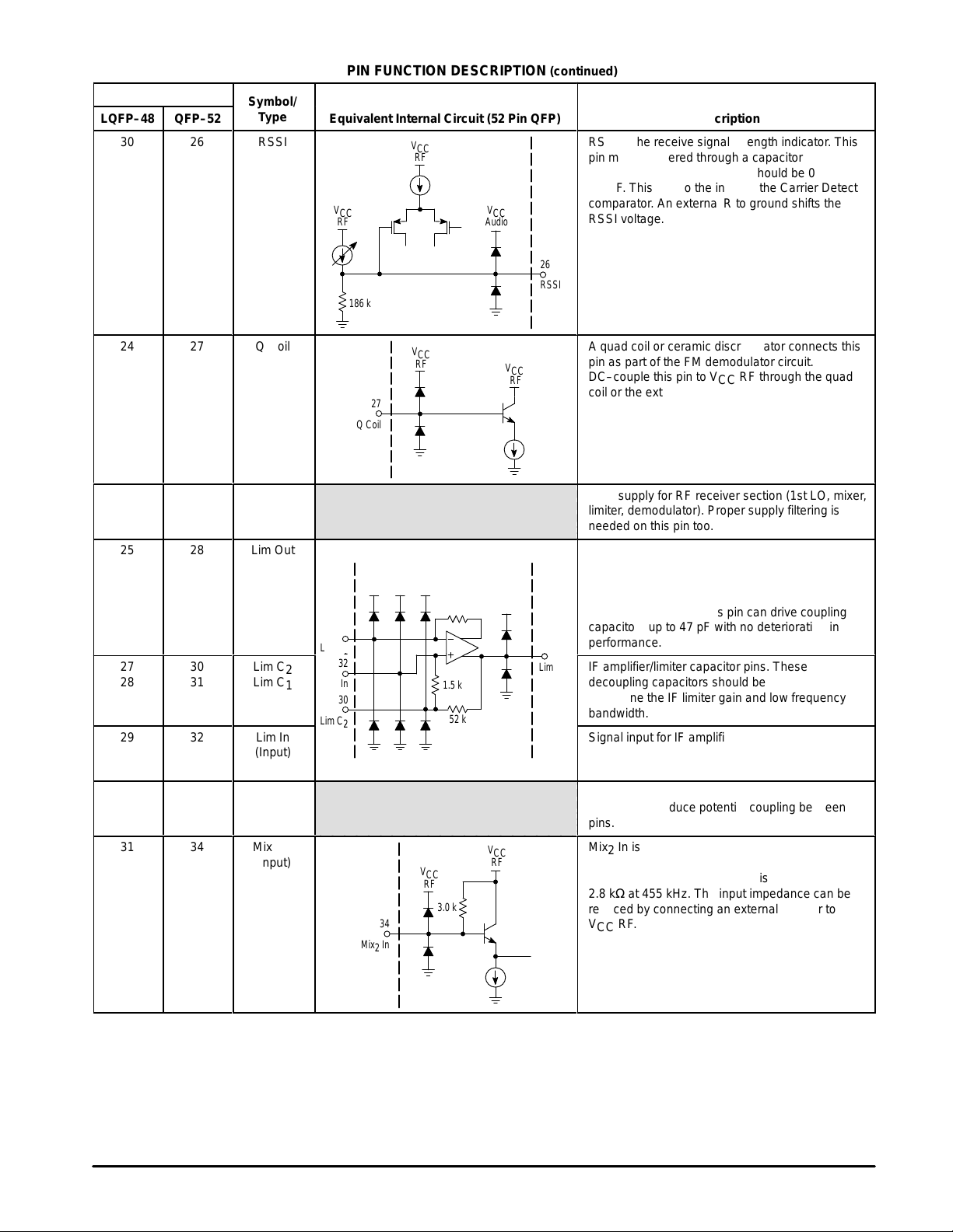
RSSI is the receive signal strength indicator. This
pin must be filtered through a capacitor to ground.
БББББББББББ
The capacitance value range should be 0.01 to
БББББББББББ
0.1 µF. This is also the input to the Carrier Detect
comparator. An external R to ground shifts the
БББББББББББ
RSSI voltage.
БББББББББББ
БББББББББББ
БББББББББББ
БББББББББББ
БББББББББББ
A quad coil or ceramic discriminator connects this
БББББББББББ
pin as part of the FM demodulator circuit.
БББББББББББ
DC–couple this pin to VCC RF through the quad
coil or the external resistor.
БББББББББББ
БББББББББББ
БББББББББББ
БББББББББББ
VCC supply for RF receiver section (1st LO, mixer,
limiter, demodulator). Proper supply filtering is
БББББББББББ
needed on this pin too.
A quad coil or ceramic discriminator are connected
to these pins as part of the FM demodulator circuit.
БББББББББББ
A coupling capacitor connects this pin to the quad
БББББББББББ
coil or ceramic discriminator as part of the FM
demodulator circuit. This pin can drive coupling
БББББББББББ
capacitors up to 47 pF with no deterioration in
БББББББББББ
performance.
IF amplifier/limiter capacitor pins. These
decoupling capacitors should be 0.1 µF. They
БББББББББББ
determine the IF limiter gain and low frequency
БББББББББББ
bandwidth.
Signal input for IF amplifier/limiter. Signals should
be ac–coupled to this pin. The input impedance is
БББББББББББ
1.5 kΩ at 455 kHz.
This pin is not connected internally but should be
БББББББББББ
grounded to reduce potential coupling between
pins.
БББББББББББ
Mix2 In is the second mixer input. Signals are to be
БББББББББББ
ac–coupled to this pin, which is biased internally to
VCC RF. The input impedance is
БББББББББББ
2.8 kΩ at 455 kHz. The input impedance can be
БББББББББББ
reduced by connecting an external resistor to
VCC RF.
БББББББББББ
БББББББББББ
БББББББББББ
БББББББББББ
14
MOTOROLA ANALOG IC DEVICE DATA
Page 15
LQFP–48
Á
Á
Á
Á
Á
Á
Á
Á
Á
Á
Á
Á
Á
Á
Á
Á
Á
Á
Á
Á
Á
Á
Á
Á
Á
Á
Á
Á
Á
Á
Á
Á
Á
Á
Á
Á
Á
Á
Á
Á
Á
Á
Á
Á
Á
Á
Á
Á
Á
Á
Á
Á
Á
Á
Á
Á
Á
Á
Á
Á
Á
Á
Á
Á
Á
Á
Á
Á
Á
Á
Á
Á
Á
Á
Á
Á
Á
950 950
Á
Á
Á
Á
Á
Á
Á
Á
Á
Á
Á
Á
Á
Á
Á
Á
Á
Á
Á
Á
Á
Á
Á
Á
Á
Á
Á
Á
Á
Á
Á
Á
Á
Á
Á
Á
Á
Á
Á
Á
Á
Á
Á
Á
Á
Á
Á
Á
Á
Á
Á
Á
Á
Á
Á
Á
Á
Á
Á
Á
Á
Á
Á
Á
Á
Á
Á
Á
Á
Á
Á
Á
Á
32
ÁÁ
ÁÁ
ÁÁ
ÁÁ
ÁÁ
Pin
QFP–52
ÁÁ
ÁÁ
ÁÁ
ÁÁ
ÁÁ
35
Symbol/
Symbol/
Type
Type
Mix2 Out
(Output)
ÁÁÁ
ÁÁÁ
ÁÁÁ
ÁÁÁ
ÁÁÁ
MC13110A/B MC13111A/B
PIN FUNCTION DESCRIPTION (continued)
Equivalent Internal Circuit (52 Pin QFP)
Equivalent Internal Circuit (52 Pin QFP)
VCC
RF
ББББББББББ
ББББББББББ
ББББББББББ
ББББББББББ
ББББББББББ
1.2 k
V
CC
RF
35
Mix2 Out
Description
Description
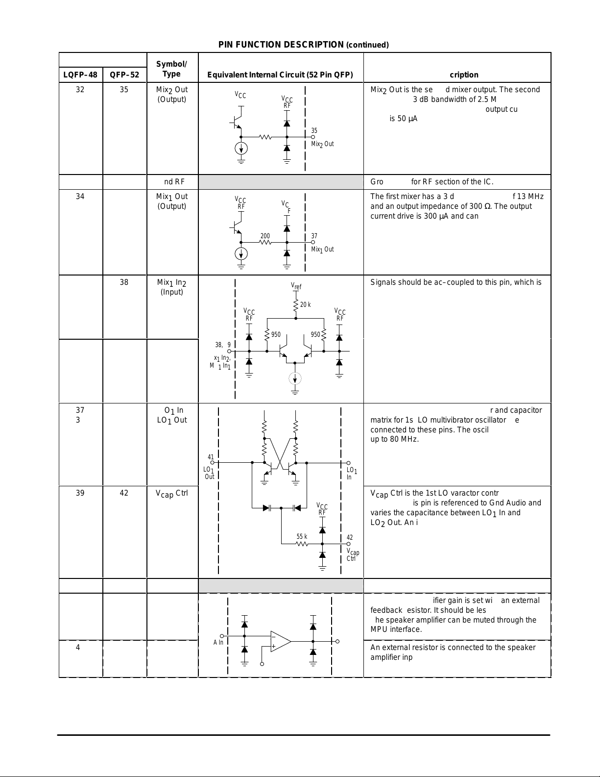
Mix2 Out is the second mixer output. The second
mixer has a 3 dB bandwidth of 2.5 MHz and an
БББББББББББ
output impedance of 1.5 kΩ. The output current
БББББББББББ
drive is 50 µA.
БББББББББББ
БББББББББББ
БББББББББББ
33
34
ÁÁ
ÁÁ
ÁÁ
ÁÁ
ÁÁ
35
ÁÁ
ÁÁ
ÁÁ
36
ÁÁ
ÁÁ
ÁÁ
37
ÁÁ
38
ÁÁ
ÁÁ
ÁÁ
ÁÁ
39
ÁÁ
ÁÁ
ÁÁ
ÁÁ
ÁÁ
40
41
ÁÁ
ÁÁ
42
ÁÁ
ÁÁ
36
37
ÁÁ
ÁÁ
ÁÁ
ÁÁ
ÁÁ
38
ÁÁ
ÁÁ
ÁÁ
39
ÁÁ
ÁÁ
ÁÁ
40
ÁÁ
41
ÁÁ
ÁÁ
ÁÁ
ÁÁ
42
ÁÁ
ÁÁ
ÁÁ
ÁÁ
ÁÁ
43
44
ÁÁ
ÁÁ
45
ÁÁ
ÁÁ
Gnd RF
Mix1 Out
(Output)
ÁÁÁ
ÁÁÁ
ÁÁÁ
ÁÁÁ
ÁÁÁ
Mix1 In
2
(Input)
ÁÁÁ
ÁÁÁ
ÁÁÁ
Mix1 In
1
(Input)
ÁÁÁ
ÁÁÁ
ÁÁÁ
LO1 In
ÁÁÁ
LO1 Out
ÁÁÁ
ÁÁÁ
ÁÁÁ
ÁÁÁ
V
Ctrl
cap
ÁÁÁ
ÁÁÁ
ÁÁÁ
ÁÁÁ
ÁÁÁ
Gnd Audio
SA Out
(Output)
ÁÁÁ
ÁÁÁ
SA In
(Input)
ÁÁÁ
ÁÁÁ
VCC
RF
ББББББББББ
ББББББББББ
ББББББББББ
ББББББББББ
ББББББББББ
ББББББББББ
V
ББББББББББ
ББББББББББ
CC
RF
V
CC
RF
200
V
950 950
ref
20 k
37
Mix1 Out
V
CC
RF
38, 39
Mix1 In2,
ББББББББББ
Mix1 In
1
ББББББББББ
ББББББББББ
ББББББББББ
ББББББББББ
ББББББББББ
41
ББББББББББ
LO
1
Out
ББББББББББ
V
55 k
V
CC
Audio
RF
CC
44
SA Out
ББББББББББ
ББББББББББ
ББББББББББ
ББББББББББ
ББББББББББ
V
CC
Audio
ББББББББББ
45
ББББББББББ
SA In
ББББББББББ
V
ББББББББББ
B
Ground pin for RF section of the IC.
The first mixer has a 3 dB IF bandwidth of 13 MHz
and an output impedance of 300 Ω. The output
БББББББББББ
current drive is 300 µA and can be programmed
БББББББББББ
for 1.0 mA.
БББББББББББ
БББББББББББ
БББББББББББ
Signals should be ac–coupled to this pin, which is
biased internally to VCC – 1.6 V. The single–ended
БББББББББББ
and differential input impedance are about 1.6 and
1.8 kΩ at 46 MHz, respectively.
БББББББББББ
БББББББББББ
БББББББББББ
БББББББББББ
БББББББББББ
Tank Elements, an internal varactor and capacitor
БББББББББББ
matrix for 1st LO multivibrator oscillator are
connected to these pins. The oscillator is useable
БББББББББББ
up to 80 MHz.
БББББББББББ
40
БББББББББББ
LO1
In
БББББББББББ
V
Ctrl is the 1st LO varactor control pin. The
cap
voltage at this pin is referenced to Gnd Audio and
БББББББББББ
varies the capacitance between LO1 In and
LO2 Out. An increase in voltage will decrease
БББББББББББ
capacitance.
42
БББББББББББ
V
cap
БББББББББББ
Ctrl
БББББББББББ
Ground for audio section of the IC.
The speaker amplifier gain is set with an external
feedback resistor. It should be less than 200 kΩ.
БББББББББББ
The speaker amplifier can be muted through the
БББББББББББ
MPU interface.
An external resistor is connected to the speaker
amplifier input (SA In). This will set the gain and
БББББББББББ
input impedance and must be ac–coupled.
БББББББББББ
MOTOROLA ANALOG IC DEVICE DATA
15
Page 16
LQFP–48
Á
Á
Á
Á
Á
Á
Á
Á
Á
Á
Á
Á
Á
Á
Á
Á
Á
Á
Á
Á
Á
Á
Á
Á
Á
Á
Á
Á
Á
Á
Á
Á
Á
Á
Á
Á
Á
Á
Á
Á
Á
Á
Á
Á
Á
Á
Á
Á
Á
Á
Á
Á
Á
Á
Á
Á
Á
Á
Á
Á
Á
Á
Á
Á
Á
Á
Á
Á
Á
Á
Á
Á
Á
Á
Á
Á
Á
Á
Á
Á
Á
Á
Á
Á
Á
Á
Á
Á
Á
Á
Á
Á
Á
Á
Á
Á
Á
Á
Á
Á
Á
Á
Á
Á
Á
Á
Á
Á
Á
Á
Á
Á
Á
Á
Á
Á
Á
Á
Á
Á
Á
Á
Á
Á
Á
Á
Á
Á
Á
Á
Á
Á
Á
Á
Á
Á
Á
Á
Á
Á
Á
Á
Á
Á
Á
Á
43
ÁÁ
ÁÁ
ÁÁ
ÁÁ
ÁÁ
44
ÁÁ
ÁÁ
ÁÁ
ÁÁ
ÁÁ
ÁÁ
45
ÁÁ
ÁÁ
ÁÁ
ÁÁ
ÁÁ
46
ÁÁ
ÁÁ
ÁÁ
ÁÁ
–
ÁÁ
ÁÁ
–
ÁÁ
ÁÁ
ÁÁ
47
ÁÁ
ÁÁ
ÁÁ
ÁÁ
Pin
QFP–52
ÁÁ
ÁÁ
ÁÁ
ÁÁ
ÁÁ
ÁÁ
ÁÁ
ÁÁ
ÁÁ
ÁÁ
ÁÁ
ÁÁ
ÁÁ
ÁÁ
ÁÁ
ÁÁ
ÁÁ
ÁÁ
ÁÁ
ÁÁ
ÁÁ
ÁÁ
ÁÁ
ÁÁ
ÁÁ
ÁÁ
ÁÁ
ÁÁ
ÁÁ
46
47
48
49
50
51
52
Symbol/
Symbol/
Type
Type
E Out
(Output)
ÁÁÁ
ÁÁÁ
ÁÁÁ
ÁÁÁ
ÁÁÁ
E Cap
ÁÁÁ
ÁÁÁ
ÁÁÁ
ÁÁÁ
ÁÁÁ
ÁÁÁ
E In
(Input)
ÁÁÁ
ÁÁÁ
ÁÁÁ
ÁÁÁ
ÁÁÁ
Scr Out
(Output)
ÁÁÁ
ÁÁÁ
ÁÁÁ
ÁÁÁ
Ref
2
ÁÁÁ
ÁÁÁ
Ref
1
ÁÁÁ
ÁÁÁ
ÁÁÁ
V
B
ÁÁÁ
ÁÁÁ
ÁÁÁ
ÁÁÁ
MC13110A/B MC13111A/B
PIN FUNCTION DESCRIPTION (continued)
Equivalent Internal Circuit (52 Pin QFP)
Equivalent Internal Circuit (52 Pin QFP)
V
CC
V
CC
V
CC
Audio
V
Audio
240
Audio
CC
30 k
V
CC
Audio
V
V
CC
Audio
47
E Cap
B
46
E Out
49
Scr Out
52
V
B
ББББББББББ
ББББББББББ
ББББББББББ
ББББББББББ
V
B
ББББББББББ
V
40 k
CC
Audio
ББББББББББ
ББББББББББ
ББББББББББ
ББББББББББ
ББББББББББ
ББББББББББ
Audio
ББББББББББ
ББББББББББ
48
E In
ББББББББББ
ББББББББББ
ББББББББББ
ББББББББББ
ББББББББББ
ББББББББББ
ББББББББББ
V
B
ББББББББББ
ББББББББББ
50, 51
Ref2, Ref
1
ББББББББББ
ББББББББББ
ББББББББББ
VCC
Audio
ББББББББББ
ББББББББББ
ББББББББББ
ББББББББББ
Description
Description
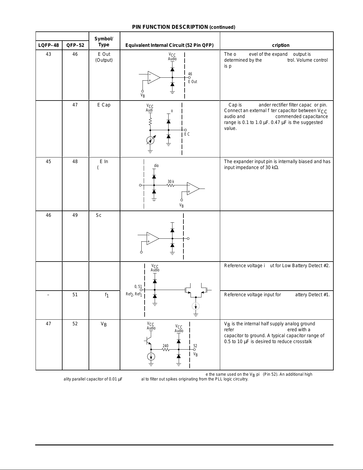
The output level of the expander output is
determined by the volume control. Volume control
БББББББББББ
is programmable through the MPU interface.
БББББББББББ
БББББББББББ
БББББББББББ
БББББББББББ
E Cap is the expander rectifier filter capacitor pin.
БББББББББББ
Connect an external filter capacitor between V
БББББББББББ
audio and E Cap. The recommended capacitance
range is 0.1 to 1.0 µF. 0.47 µF is the suggested
БББББББББББ
value.
БББББББББББ
БББББББББББ
БББББББББББ
CC
The expander input pin is internally biased and has
input impedance of 30 kΩ.
БББББББББББ
БББББББББББ
БББББББББББ
БББББББББББ
БББББББББББ
Scr Out is the Rx audio output. An internal low
pass filter has a –3 dB bandwidth of 4.0 kHz.
БББББББББББ
БББББББББББ
БББББББББББ
БББББББББББ
Reference voltage input for Low Battery Detect #2.
БББББББББББ
БББББББББББ
Reference voltage input for Low Battery Detect #1.
БББББББББББ
БББББББББББ
БББББББББББ
VB is the internal half supply analog ground
reference. This pin must be filtered with a
БББББББББББ
capacitor to ground. A typical capacitor range of
0.5 to 10 µF is desired to reduce crosstalk and
БББББББББББ
noise. It is important to keep this capacitor value
equal to the PLL V
БББББББББББ
(Note 9).
БББББББББББ
capacitor due to logic timing
ref
NOTE: 9.A capacitor range of 0.5 to 10 µF is recommended. The capacitor value should be the same used on the VB pin (Pin 52). An additional high
ББББББББББББББББББББББББББББББББ
16
quality parallel capacitor of 0.01 µF is essential to filter out spikes originating from the PLL logic circuitry.
MOTOROLA ANALOG IC DEVICE DATA
Page 17
MC13110A/B MC13111A/B
ББББББББББББББББ
Á
ББББББББББББББББ
Á
DEVICE DESCRIPTION AND APPLICATION INFORMATION
The following text, graphics, tables and schematics are
provided to the user as a source of valuable technical
information about the Universal Cordless Telephone IC. This
information originates from thorough evaluation of the device
performance for the US and French applications. This data
was obtained by using units from typical wafer lots. It is
important to note that the forgoing data and information was
from a limited number of units. By no means is the user to
assume that the data following is a guaranteed parametric.
Only the minimum and maximum limits identified in the
electrical characteristics tables found earlier in this spec are
guaranteed.
General Circuit Description
The MC131 10A/B and MC13111A/B are a low power dual
conversion narrowband FM receiver designed for
applications up to 80 MHz carrier frequency. This device is
primarily designated to be used for the 49 MHz cordless
phone (CT–0), but has other applications such as low data
rate narrowband data links and as a backend device for 900
MHz systems where baseband analog processing is
required. This device contains a first and second mixer,
limiter, demodulator, extended range receive signal strength
(RSSI), receive and transmit baseband processing, dual
programmable PLL, low battery detect, and serial interface
for microprocessor control. The FM receiver can also be
used with either a quadrature coil or ceramic resonator.
Refer to the Pin Function Description table for the simplified
internal circuit schematic and description of this device.
DC Current and Battery Detect
Figures 3 through 6 are the current consumption for
Inactive, Standby , Receive, and Active modes versus supply
voltages. Figures 7 and 8 show the typical behavior of current
consumption in relation to temperature. The relationship of
additional current draw due to IP3 bit set to <1> and supply
voltage are shown in Figures 9 and 10.
For the Low Battery Detect, the user has the option to
operate the IC in the programmable or non–programmable
modes. Note that the 48 pin package can only be used in the
programmable mode. Figure 128 describes this operation
(refer to the Serial Interface section under Clock Divider
Register).
In the programmable mode several different internal
threshold levels are available (Figure 2). The bits are set
through the SCF Clock Divider Register as shown in Figures
108 and 126. The reference for the internal divider network is
VCC Audio. The voltages on the internal divider network are
compared to the Internal Reference Voltage, VB, generated
by an internal source. Since the internal comparator used is
non–inverting, a high at VCC Audio will yield a high at the
battery detect output, and vice versa for VCC Audio set to a
low level. For the 52 pin package option, the Ref 1 and Ref 2
pins need to be tied to VCC when used in the programmable
mode. It is essential to keep the external reference pins
above Gnd to prevent any possible power–on reset to be
activated.
When considering the non–programmable mode (bits set
to <000>) for the 52 pin package, the Ref 1 and Ref 2 pins
become the comparators reference. An internal switch is
activated when the non–programmable mode is chosen
connecting Ref 1 and Ref 2. Here, two external precision
resistor dividers are used to set independent thresholds for
two battery detect hysteresis comparators. The voltages on
Ref 1 and Ref 2 are again compared to the internally
generated 1.5 V reference voltage (VB).
The Low Battery Detect threshold tolerance can be
improved by adjusting a trim–pot in the external resistor
divider (user designed). The initial tolerance of the internal
reference voltage (VB) is ±6.0%. Alternately , the tolerance of
the internal reference voltage can be improved to ±1.5%
through MPU serial interface programming (refer to the Serial
Interface section, Figure 131). The internal reference can be
measured directly at the “VB” pin. During final test of the
telephone, the VB internal reference voltage is measured.
Then, the internal reference voltage value is adjusted
electronically through the MPU serial interface to achieve the
desired accuracy level. The voltage reference register value
should be stored in ROM during final test so that it can be
reloaded each time the combo IC is powered up. The Low
Battery Detect outputs are open collector. The battery detect
levels will depend on the accuracy of the VB voltage. Figure
12 indicates that the VB voltage is fairly flat over temperature.
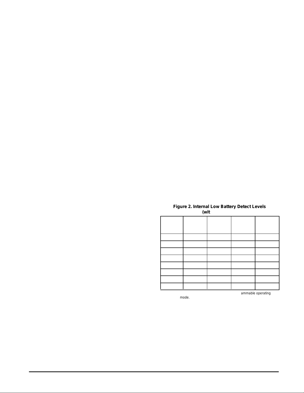
Figure 2. Internal Low Battery Detect Levels
БББББББББББББББ
Battery
Detect
Select
0 – – – –
1 2.867 2.861 2.864 4.0
2 2.953 2.947 2.950 6.0
3 3.039 3.031 3.035 8.0
4 3.207 3.199 3.204 8.0
5 3.291 3.285 3.288 6.0
6 3.375 3.367 3.371 8.0
7 3.461 3.453 3.457 8.0
NOTE: 10. Battery Detect Select 0 is the non–programmable operating
БББББББББББББББ
Ramping
mode.
(with VB = 1.5 V)
Ramping
Up
(V)
Down
(V)
Average
(V)
Hysteresis
(mV)
MOTOROLA ANALOG IC DEVICE DATA
17
Page 18

MC13110A/B MC13111A/B
Figure 3. Current versus Supply
40
A)
35
µ
30
25
20
15
IC, SUPPLY CURRENT (
10
INACT
5.0
I
0
2.7 3.1 3.5 3.9 4.3 4.7 5.1 5.5
V oltage Inactive Mode
VCC, SUPPLY VOLTAGE (V)
DC CURRENT
, SUPPLY CURRENT (mA)
CC
STD I
Figure 4. Current versus Supply
V oltage Standby Mode, MCU
Clock Output – On at 2.048 MHz
1.0
0.9
0.8
0.7
0.6
0.5
0.4
0.3
0.2
0.1
0
2.7 3.1 3.5 3.9 4.3 4.7 5.1 5.5
VCC, SUPPLY VOLTAGE (V)
MCU Clock Out On
MCU Clock Out Off
Figure 5. Current versus Supply
V oltage Receive Mode
5.0
4.9
4.8
4.7
4.6
4.5
4.4
, SUPPLY CURRENT (mA)
4.3
CC
I
4.2
x
R
4.1
4.0
2.7 3.1 3.5 3.9 4.3 4.7 5.1 5.5
VCC, SUPPLY VOLTAGE (V)
MCU Clock Out On
MCU Clock Out Off
Figure 7. Current versus
T emperature Normalized to 25°C
15
°
10
5.0
0
–5.0
DELTA CURRENT DRAIN (% FROM 25 C)
–10
–40 –30 –20 –10 0 10 20 30 40 50 60 70 80 90
°
TA, TEMPERATURE (
C)
Standby
Inactive
Figure 6. Current versus Supply V oltage
Active Mode
8.0
7.9
7.8
7.7
7.6
7.5
7.4
7.3
CC
7.2
ACT I , SUPPLY CURRENT (mA)
7.1
7.0
2.7 3.1 3.5 3.9 4.3 4.7 5.1 5.5
VCC, SUPPLY VOLTAGE (V)
MCU Clock Out On
MCU Clock Out Off
Figure 8. Current versus
T emperature Normalized to 25°C
6.0
°
4.0
2.0
0
–2.0
–4.0
–6.0
–8.0
–10
DELTA CURRENT DRAIN (% FROM 25 C)
–12
–40 –30 –20 –10 10 20 30 40 50 60 70 80 90
0
TA, TEMPERATURE (
°
C)
Receive
Active
18
MOTOROLA ANALOG IC DEVICE DATA
Page 19
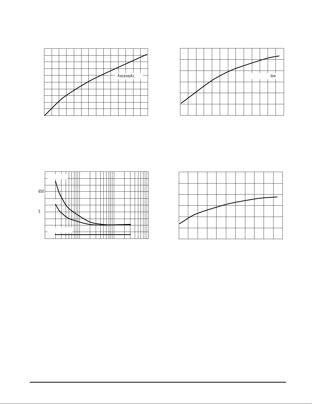
MC13110A/B MC13111A/B
Figure 9. Additional Supply Current Consumption
1.50
1.48
1.46
1.44
1.42
1.40
1.38
1.36
1.34
DELTA CURRENT DRAIN (mA)
1.32
1.30
2.7 2.9 3.1 3.3 3.5 3.7 3.9 4.1 4.3 4.5 4.7 4.9 5.1 5.3 5.5
versus Supply V oltage, IP3 = <1>
Receive/Active
VCC, SUPPLY VOLTAGES (V)
DC CURRENT
°
DELTA CURRENT DRAIN (% FROM 25 C)
Figure 10. Additional IP3
Supply Current Consumption versus
T emperature Normalized to 25°C
10
5
0
Receive/Active
–5
–10
–15
–20
–40 –30 –20 –10 0 10 20 30 40 50 60 70 80 90
TA, TEMPERATURE (
°
C)
Figure 11. Current Standby
800
750
700
650
600
550
500
450
CC
400
STD I , SUPPLY CURRENT (mA)
350
300
1.0 10 100 1000
Mode versus MCU Clock Output
10 pF load
No load
MCU clock off
MCU CLK OUT DIVIDE VALUE
Figure 12. VB V oltage versus Temperature
Normalized to 1.5 V at 25°C
1.5075
1.5050
1.5025
1.5000
1.4975
1.4950
s
V , NORMALIZED VB VOLTAGE (V)
1.4925
–20–100 102030405060708090
°
TA, TEMPERATURE (
C)
MOTOROLA ANALOG IC DEVICE DATA
19
Page 20
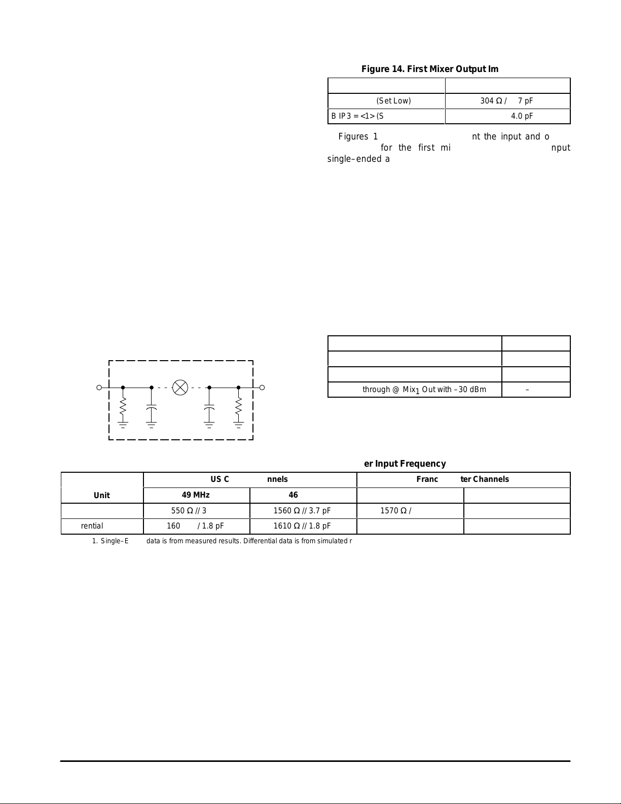
MC13110A/B MC13111A/B
ББББББББББББББББ
ББББББББ
ББББББББ
ББББББББ
ББББББББББББББББ
ББББББББББББ
ББББББББББББ
ББББББББББББ
ББББББББББББ
БББББББ
БББББББ
БББББББ
FIRST AND SECOND MIXER
Mixer Description
The 1st and 2nd mixers are similar in design. Both are
double balanced to suppress the LO and the input
frequencies to give only the sum and difference frequencies
at the mixer output. Typically the LO is suppressed better
than –50 dB for the first mixer and better than –40 dB for the
second mixer. The gain of the 1st mixer has a –3.0 dB corner
at approximately 13 MHz and is used at a 10.7 MHz IF . It has
an output impedance of 300 Ω and matches to a typical
10.7 MHz ceramic filter with a source and load impedance of
330 Ω. A series resistor may be used to raise the impedance
for use with crystal filters. They typically have an input
impedance much greater than 330 Ω.
First Mixer
Figures 17 through 20 show the first mixer transfer curves
for the voltage conversion gain, output level, and
intermodulation. Notice that there is approximately 10 dB
linearity improvement when the “IP3 Increase” bit is set to
<1>. The “IP3 Increase” bit is a programmable bit as shown in
the Serial Programmable Interface section under the R
Counter Latch Register. The IP3 = <1> option will increase
the supply current demand by 1.3 mA.
Figure 13. First Mixer Input and Output Impedance
Schematic
1st Mixer
Mix1 In Mix1 Out
R
C
PI
C
PI
PO
R
PO
БББББББББББББББ
БББББББ
БББББББ
БББББББ
Figure 14. First Mixer Output Impedance
Unit
B IP3 = <0> (Set Low)
B IP3 = <1> (Set High)
БББББББ
БББББББ
БББББББ
Output Impedance
304 Ω // 3.7 pF
300 Ω // 4.0 pF
Figures 13, 14, and 16 represent the input and output
impedance for the first mixer. Notice that the input
single–ended and differential impedances are basically the
same. The output impedance as described in Figure 14 will
be used to match to a ceramic or crystal filter’s input
impedance. A typical ceramic filter input impedance is 330 Ω
while crystal filter input impedance is usually 1500 Ω. Exact
impedance matching to ceramic filters are not critical,
however, more attention needs to be given to the filter
characteristics of a crystal filter. Crystal filters are much
narrower. It is important to accurately match to these filters to
guaranty a reasonable response.
T o find the IF bandwidth response of the first mixer refer to
Figure 22. The –3.0 dB bandwidth point is approximately 13
x
MHz. Figure 15 is a summary of the first mixer feedthrough
parameters.
Figure 15. First Mixer Feedthrough Parameters
Parameter
1st LO Feedthrough @ Mix1 In
1st LO Feedthrough @ Mix1 Out
RF Feedthrough @ Mix1 Out with –30 dBm
1
(dBm)
–70.0
–55.5
–61.0
Figure 16. First Mixer Input Impedance over Input Frequency
US Center Channels
Unit
Single–Ended
Differential
Note: 1 1. Single–Ended data is from measured results. Differential data is from simulated results.
49 MHz
1550 Ω // 3.7 pF
1600 Ω // 1.8 pF
46 MHz
1560 Ω // 3.7 pF
1610 Ω // 1.8 pF
France Center Channels
41 MHz
1570 Ω // 3.8 pF
1670 Ω // 1.8 pF
26 MHz
1650 Ω // 3.7 pF
1710 Ω // 1.8 pF
20
MOTOROLA ANALOG IC DEVICE DATA
Page 21
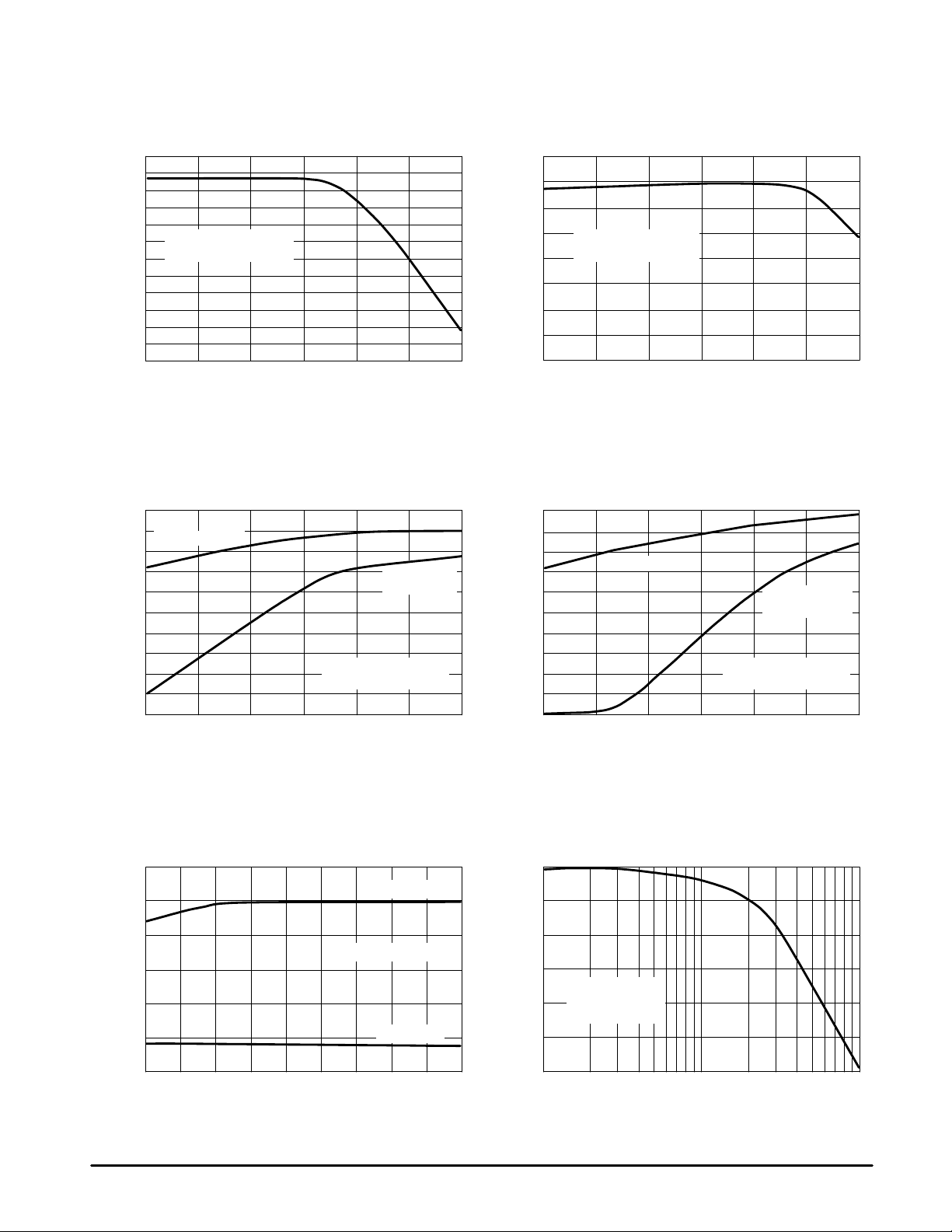
MC13110A/B MC13111A/B
FIRST MIXER
Figure 17. First Mixer V oltage Conversion
14
12
10
VCC = 3.6 V
, VOLTAGE
gain1
MX
CONVERSION GAIN (dB)
IF = 10.695 MHz, 330
8.0
6.0
4.0
2.0
–40
Figure 19. First Mixer Output Level and
0
Fundamental Level
–20
–40
Out, MIXER OUTPUT (dBm)
1
Mix
Gain, IP3_bit = 0
Ω
Mix1 In, MIXER INPUT LEVEL (dBm)
Intermodulation, IP3_bit = 0
3rd Order
Intermodulation
VCC = 3.6 V
IF = 10.695 MHz, 330
Figure 18. First Mixer V oltage Conversion
Gain, IP3_bit = 1
14
12
VCC = 3.6 V
10
, VOLTAGE
gain1
MX
8.0
CONVERSION GAIN (dB)
6.0
–40
IF = 10.695 MHz, 330
–35–35 –30–30 –25–25 –20–20 –15–15 –10–10
Mix1 In, MIXER INPUT LEVEL (dBm)
Ω
Figure 20. First Mixer Output Level and
Intermodulation, IP3_bit = 1
0
–20
–40
–60–60
Out, MIXER OUTPUT (dBm)
1
Ω
Mix
–80–80
Fundamental Level
3rd Order
Intermodulation
VCC = 3.6 V
IF = 10.695 MHz, 330
Ω
–40
–35 –30–30 –25–25 –20
Mix1 In, MIXER INPUT LEVEL (dBm)
Figure 21. First Mixer Compression versus
–10
–12
–14
, 1.0 dB
1
–16
1.0 dB Mix
–18
O
V
–20
VOLTAGE COMPRESSION (dBm)
2.7
3.3
VCC Audio, AUDIO SUPPLY VOLTAGE (V)
–20 –15
Supply V oltage
IF = 10.695 MHz, 330
4.2
–15 –10
–10
–100–100
–40
–35
Mix1 In, MIXER INPUT LEVEL (dBm)
Figure 22. First IF Bandwidth
15
IP3_bit = 1
IP3_bit = 0
4.8
Ω
5.4
10
5.0
0
, VOLTAGE
gain1
–5.0
MX
CONVERSION GAIN (dB)
–10
–15–22
VCC = 3.6 V
RL = 330
LO = 36.075 MHz
1.0
Ω
10
f, IF FREQUENCY (MHz)
1003.6 3.9 4.53.0 5.1
MOTOROLA ANALOG IC DEVICE DATA
21
Page 22

MC13110A/B MC13111A/B
Á
Á
Á
Á
ББББББББББББББББ
Á
ББББББББББББ
Á
Á
ББББББББББББ
Á
Á
ББББББББББББ
Á
Á
Second Mixer
Figures 26 through 29 represents the second mixer
transfer characteristics for the voltage conversion gain,
output level, and intermodulation. There is a slight
improvement in gain when the “IP3 bit” is set to <1> for the
second mixer. (Note: This is the same programmable bit
discussed earlier in the section.)
Figure 23. Second Mixer Input and Output
Impedance Schematic
2nd Mixer
Mix2 In Mix2 Out
R
Figure 24. Second Mixer Input and Output
БББББББББББББББ
БББББ
Unit
IP3 = <0> (Set Low)
IP3 = <1> (Set High)
C
PI
PI
Impedances
Input Impedance
ÁÁÁÁ
RPI // C
2817 Ω // 3.6 pF
2817 Ω // 3.6 pF
PO
R
PO
C
Output
Impedance
ÁÁÁÁ
PI
RPO // C
PO
1493 Ω // 6.1 pF
1435 Ω // 6.2 pF
The 2nd mixer input impedance is typically 2.8 kΩ. It
requires an external 360 Ω parallel resistor for use with a
standard 330 Ω, 10.7 MHz ceramic filter. The second mixer
output impedance is 1.5 kΩ making it suitable to match
standard 455 kHz ceramic filters.
The IF bandwidth response of the second mixer is shown
in Figure 31. The –3.0 dB corner is 2.5 MHz. The feedthrough
parameters are summarized in Figure 25.
Figure 25. Second Mixer Feedthrough Parameters
БББББББББББББББ
БББББББББББ
2nd LO Feedthrough @ Mix2 Out
БББББББББББ
IF Feedthrough @ Mix2 Out with –30 dBm
БББББББББББ
Parameter
(dBm)
ÁÁÁ
–42.9
ÁÁÁ
–61.7
ÁÁÁ
22
MOTOROLA ANALOG IC DEVICE DATA
Page 23

MC13110A/B MC13111A/B
SECOND MIXER
Figure 26. Second Mixer Conversion Gain,
22
20
18
, VOLTAGE
16
gain2
CONVERSION GAIN (dB)
14
12
VCC = 3.6 V
IF = 455 kHz
RL = 1500
Figure 28. Second Mixer Output Level and
Intermodulation, IP3_bit = 0
10
Fundamental Level
–10
–30
IP3_bit = 0
Ω
Mix2 In, MIXER INPUT LEVEL (dBm)
3rd Order
Intermodulation
Figure 27. Second Mixer Conversion Gain,
22
20
18
, VOLTAGE
gain2
MX
16
CONVERSION GAIN (dB)
14
–40–40
VCC = 3.6 V
IF = 455 kHz
RL = 1500
–35–35 –30–30 –25–25 –20–20 –15–15 –10–10
Figure 29. Second Mixer Output Level and
Intermodulation, IP3_bit = 1
10
Fundamental Level
–10
–30
IP3_bit = 1
Ω
Mix2 In, MIXER INPUT LEVEL (dBm)
3rd Order
Intermodulation
–50
Out, MIXER OUTPUT (dBm)V
2
–70
Mix
–90
–40
–35 –30–30 –25–25 –20
Mix2 In, MIXER INPUT LEVEL (dBm)
Figure 30. Second Mixer Compression
versus Supply V oltage
–10
–12
–14
, 1.0 dB MX
2
–16
–18
1.0 dB Mix
O
–20
VOLTAGE COMPRESSION (dBm)
–22
3.3
VCC Audio, AUDIO SUPPLY VOLTAGE (V)
–50
VCC = 3.6 V
IF = 455 kHz
RL = 1500
–20 –15
Ω
–15 –10
–10
Out, MIXER OUTPUT (dBm)
2
–70
Mix
–90
–40
–35
Mix2 In, MIXER INPUT LEVEL (dBm)
Figure 31. Second IF Bandwidth
25
4.2
IP3_bit = 1
IP3_bit = 0
IF = 455 kHz
RL = 1500
Ω
4.8
5.4
20
15
, VOLTAGE
10
gain2
MX
CONVERSION GAIN (dB)
5.0
0
0.12.7
VCC = 3.6 V
RL = 1500
Ω
1.0
f, IF FREQUENCY (MHz)
VCC = 3.6 V
IF = 455 kHz
RL = 1500
Ω
103.6 3.9 4.53.0 5.1
MOTOROLA ANALOG IC DEVICE DATA
23
Page 24

MC13110A/B MC13111A/B
First Local Oscillator
The 1st LO is a multi–vibrator oscillator. The tank circuit is
composed of a parallel external capacitance and inductance,
internal programmable capacitor matrix, and internal
varactor. The local oscillator requires a voltage controlled
input to the internal varactor and an external loop filter driven
by on–board phase–lock control loop (PLL). The 1st LO
internal component values have a tolerance of ±15%. A
typical dc bias level on the LO Input and LO Output is 0.45
Vdc. The temperature coefficient of the varactor is
+0.08%/°C. The curve in Figure 33 is the varactor control
voltage range as it relates to varactor capacitance. It
represents the expected internal capacitance for a given
control voltage (V
MC131 1 1A/B. Figure 32 shows a representative schematic of
the first LO function.
Figure 32. First Local Oscillator Schematic
1st LO
Programmable
Internal
Capacitor
Ctrl) of the MC13110A/B and
cap
V
Ctrl
cap
Varactor
Varactor
LO1 In
LO1 Out
C
ext
L
ext
T o select the proper L
ext
and C
we can do the following
ext
analysis. From Figure 34 it is observed that an inductor will
have a significant affect on first LO performance, especially
over frequency. The overall minimum Q required for first LO
to function as it relates to the LO frequency is also given in
Figure 34.
Choose an inductor value, say 470 nH. From Figure 34,
the minimum operating Q is approximately 25. From the
following equation:
Q Coil = Rp/X Coil
where: Rp = parallel equivalent impedance (Figure 35).
C
can be determined as follows:
ext
fLO+
where: L
ext
1
Ǹ
2pL
extCext
= external inductance, C
= external
ext
capacitance.
Figure 34 clearly indicates that for lower coil values, higher
quality factors (Q) are required for the first LO to function
properly. Also, lower LO frequencies need higher Q’s. In
Figure 35 the internal programmable capacitor selection
relative to the first LO frequency and the parallel impedance
is shown. This information will help the user to decide what
inductor (L
) to choose for best performance in terms of Q.
ext
Refer to the Auxiliary Register in the Serial Interface
Section for further discussion on LO programmability .
24
MOTOROLA ANALOG IC DEVICE DATA
Page 25

MC13110A/B MC13111A/B
FIRST LOCAL OSCILLATOR
Figure 33. First LO Varicap Capacitance
versus Control Voltage
15
14
13
12
11
10
, CAPACITANCE (pF)
cap
9.0
V
8.0
7.0
0
0.5 1.0 1.5 2.0 2.5 3.0 3.5 4.0 4.5 5.0 5.5
V
, CONTROL VOLTAGE (V)
capCtrl
Figure 35. Representative Parallel Impedance
versus Capacitor Select
100
Figure 34. First LO Minimum Required Overall
Q Value versus Inductor Value
120
100
0
100
30 MHz
40 MHz
50 MHz
LO INDUCTOR VALUE (nH)
80
60
40
OVERALL MINIMUM Q VALUE
20
Figure 36. Varicap Value at VCV = 1.0 V
Over Temperature
11
10.6
1000
Ω
IMPEDANCE (k )
, REPRESENTATIVE PARALLEL
P
R
10
0
1 6 4 3 8 9 10 11 12 13 14 15257
Channel Number, U.S. Handset Application
1.8
1.7
Cap 11
1.6
1.5
1.4
1.3
1.2
Ctrl, CONTROL VOL TAGE (V)V
1.1
cap
1.0
0.9
1
3 5 7 9 11 13 15 17 19 21 23 25
CH1–CH25, U.S. HANDSET CHANNEL APPLICATION
C1–C15, CAPACITANCE SELECT
Figure 37. Control Voltage versus
Cap 10
Cap 9
30 MHz
40 MHz
50 MHz
Cap 6
10.2
9.8
, CAPACITANCE (pF)
cap
V
9.4
9.8
–20 0 25 70 8555
TA, AMBIENT TEMPERATURE (°C)
Figure 38. Control Voltage versus
Channel Number, U.S. Baseset Application
1.8
1.7
1.6
1.5
1.4
1.3
1.2
1.1
Ctrl, CONTROL VOL TAGE (V)
1.0
cap
V
0.9
0.8
1 3 5 7 9 11 13 15 17 19 21 23 25
Cap 8
Cap 3
CH1–CH25, U.S. BASESET CHANNEL APPLICATION
Cap 4
MOTOROLA ANALOG IC DEVICE DATA
25
Page 26

MC13110A/B MC13111A/B
Á
Second Local Oscillator
The 2nd LO is a CMOS oscillator. It is used as the PLL
reference oscillator and local oscillator for the second
frequency conversion in the RF receiver. It is designed to
utilize an external parallel resonant crystal. See schematic in
Figure 39.
Figure 39. Second Local Oscillator Schematic
2nd LO
R
Figure 40. Second Local Oscillator
БББББББББББББББ
Input Impedance (RPI // CPI)
Output Impedance (RPO // CPO)
C
PI
PI
Gm
LO2 In LO2 Out
Xtal
C
1
C
Input and Output Impedance
R
PO
PO
C
2
11.6 kΩ // 2.9 pF
9.6 kΩ // 2.7 pF
Figure 41 shows a typical gain/phase response of the
second local oscillator. Load capacitance (CL), equivalent
series resistance (ESR), and even supply voltage will have
and affect on the 2nd LO response as shown in Figures 45
and 46. Except for the standby mode open loop gain is fairly
constant as supply voltage increases from 2.5 V. This is due
to the regulated voltage of 2.5 V on PLL V
. From the graphs
ref
it can seen that optimum performance is achieved when C1
equals C2 (C1/C2 = 1).
Figure 46 represents the ESR versus crystal load
capacitance for the 2nd LO. This relationship was defined by
using a 6.0 dB minimum loop gain margin at 3.6 V. This is
considered the minimum gain margin to guarantee oscillator
start–up.
Oscillator start–up is also significantly affected by the
crystal load capacitance selection. In Figures 42 and 43 the
relationship between crystal load capacitance, supply
voltage, and external load capacitance ratio (C2/C1), can be
seen. The lower the load capacitance the better the
performance.
Given the desired crystal load capacitance, C1 and C2
can be determined from Figure 47. It is also interesting to
point out that current consumption increases when C1 ≠ C2,
as shown in Figure 44.
Be careful not to overdrive the crystal. This could cause a
noise problem. An external series resistor on the crystal
output can be added to reduce the drive level, if necessary.
, LO VOLTAGE GAIN (dB)
gain2
V
SECOND LOCAL OSCILLATOR
Figure 41. Second LO Gain/Phase @ –10 dBm
15
10
10.24 MHz Crystal
5.0
CL = 10 pF
RS = 20
0
C1 = C2 = 15 pF
–5.0
–10
–15
–20
–25
10.235
Ω
f, FREQUENCY (MHz)
Gain
Phase
10.24 10.245
90
67.5
45
22.5
0
–22.5
–45
–67.5
–90
Figure 42. Start–Up Time versus Capacitor
Ratio, Inactive to Rx Mode
6.0
10.24 MHz Crystal
CL = 10 pF
5.0
4.0
3.0
2.0
STAR T–UP TIME (ms)
1.0
0
0
Ω
RS = 20
0.5 1.0 1.5 2.0 2.5 3.0 3.5 4.0
CAPACITOR RA TIO (C2:C1)
VCC = 2.3 V
VCC = 2.7 V
VCC = 3.6 V
VCC = 5.0 V
26
MOTOROLA ANALOG IC DEVICE DATA
Page 27

MC13110A/B MC13111A/B
SECOND LOCAL OSCILLATOR
30
25
20
15
10
STAR T–UP TIME (ms)
5.0
, SECOND OSCILLAT OR LEVEL (dBm)
2
LO
0
20
16
Figure 43. Start–Up Time versus Capacitor
Ratio, Inactive to Rx Mode
10.24 MHz Crystal
CL = 24 pF
Ω
RS = 16
0
0.5 0.5
1.0 1.0
1.5 1.5
2.0 2.0
2.5 2.5
CAPACITOR RA TIO (C2:C1)
VCC = 2.3 V
VCC = 2.7 V
VCC = 3.6 V
VCC = 5.0 V
3.0 3.0
3.5 3.5
4.0 4.0
µ
, STANDBY CURRENT ( A)
I
Figure 45. Maximum Open Loop Gain
versus Capacitor Ratio
Ω
VCC = 2.7, 3.6, 5.0 V
Figure 44. Second LO Current Consumption
versus Capacitor Ratio
800
700
600
500
400
300
200
10.24 MHz Crystal
STD
100
CL = 10 pF
RS = 20
0
0
Standby Current with Clk_Out
Running at 2.048 MHz
Standby Current
with Clk_Out Off
Ω
CAPACITOR RA TIO (C2:C1)
Figure 46. Maximum Allowable
Equivalent Series Resistance (ESR)
versus Crystal Load Capacitance
1000
13
12
11
10
Oscillator Level
9.0
12
8.0
10.24 MHz Crystal
CL = 10 pF
4.0
AVOL, OPEN LOOP GAIN (dB)
RS = 20
Rx Mode
0
0
0.5
Ω
1.0
1.5
CAPACITOR RA TIO (C2:C1)
2.0
OPTIMUM C1 AND C2 VALUE (pF)
2.5
VCC = 2.3 V
3.0
3.5
4.0
100
ESR, EQUIVALENT RESISTANCE ( )
10
10
Figure 47. Optimum Value for C1 and C2
versus Equivalent Required Parallel
Capacitance of the Crystal
70
60
50
40
30
20
10
C1 = C2
Curve Valid for f
12 14 16 18 20 22 24 26 28 30 32
in the Range of 10 MHz to 12 MHz
osc
CRYSTAL LOAD CAPACITANCE (pF)
0
0
MOTOROLA ANALOG IC DEVICE DATA
5.0 10 15 20 30 3525
REQUIRED P ARALLEL CR YSTAL LOAD CAPACITANCE (pF)
27
Page 28

MC13110A/B MC13111A/B
Á
Á
IF Limiter and Demodulator
The limiting IF amplifier typically has about 1 10 dB of gain;
the frequency response starts rolling off at 1.0 MHz.
Decoupling capacitors should be placed close to Pins 31 and
32 to ensure low noise and stable operation. The IF input
impedance is 1.5 kΩ. This is a suitable match to 455 kHz
ceramic filters.
Figure 48. IF Limiter Schematic
Limiter Stage
Lim OutLim In
R
C
PI
БББББББББББББББ
БББББ
Lim In
Figure 49. Limiter Input Impedance
Input Impedance
Unit
БББББ
Figure 50. Quadrature Detector
Demodulator Schematic
C
28
10 p
1
The quadrature detector is coupled to the IF with an
external capacitor between Pins 27 and 28. Thus, the
recovered signal level output is increased for a given
bandwidth by increasing the capacitor. The external
quadrature component may be either a LCR resonant circuit,
which may be adjustable, or a ceramic resonator which is
usually fixed tuned. (More on ceramic resonators later.)
The bandwidth performance of the detector is controlled
by the loaded Q of the LC tank circuit (Figure 50). The
following equation defines the components which set the
detector circuit’s bandwidth:
(1) RT = Q XL,
where RT is the equivalent shunt resistance across the LC
tank. XL is the reactance of the quadrature inductor at the IF
frequency (XL= 2π f L).
The 455 kHz IF center frequency is calculated by:
(2) fc = [2π (L Cp)
1/2
where L is the parallel tank inductor. Cp is the equivalent
parallel capacitance of the parallel resonant tank circuit.
The following is a design example for a detector at 455
kHz and a specific loaded Q:
The loaded Q of the quadrature detector is chosen
somewhat less than the Q of the IF bandpass for margin. For
an IF frequency of 455 kHz and an IF bandpass of 20 kHz,
R
22.1 k
] – 1
PI
(RPI)
1538 Ω
ext
Input Impedance
ÁÁÁÁ
Toko Q Coil
7MCS–8128Z
(CPI)
15.7 pF
Q CoilLim Out
the IF bandpass Q is approximately 23; the loaded Q of the
quadrature tank is chosen slightly lower at 15.
Example:
Let the total external C = 180 pF. (Note: the capacitance is
the typical capacitance for the quad coil.) Since the external
capacitance is much greater than the internal device and
PCB parasitic capacitance, the parasitic capacitance may be
neglected.
Rewrite equation (2) and solve for L:
2
L = (0.159)2/(C f
)
c
L = 678 µH ; Thus, a standard value is chosen:
L = 680 µH (surface mount inductor)
The value of the total damping resistor to obtain the
required loaded Q of 15 can be calculated from equation (1):
RT = Q(2π f L)
RT = 15(2π)(0.455)(680) = 29.5 kΩ
The internal resistance, R
at the quadrature tank Pin 27
int
is approximately 100 kΩ and is considered in determining the
external resistance, R
R
= ((RT)(R
ext
R
= 41.8 kΩ;Thus, choose a standard value:
ext
R
= 39 kΩ
ext
In Figure 50, the R
which is calculated from:
ext
))/(R
int
– RT)
int
is chosen to be 22.1 kΩ. An
ext
adjustable quadrature coil is selected. This tank circuit
represents one popular network used to match to the
455 kHz carrier frequency. The output of the detector is
represented as a “S–curve” as shown in Figure 52. The goal
is to tune the inductor in the area that is most linear on the
“S–curve” (minimum distortion) to optimize the performance
in terms of dc output level. The slope of the curve can also be
adjusted by choosing higher or lower values of R
. This will
ext
have an affect on the audio output level and bandwidth. As
R
is increased the detector output slope will decrease.
ext
The maximum audio output swing and distortion will be
reduced and the bandwidth increased. Of course, just the
opposite is true for smaller R
ext
.
A ceramic discriminator is recommended for the
quadrature circuit in applications where fixed tuning is
desired. The ceramic discriminator and a 5.6 kΩ resistor are
placed from Pin 27 to VCC . A 22 pF capacitor is placed from
Pin 28 to 27 to properly drive the discriminator. MuRata Erie
has designed a resonator for this part (CDBM455C48 for
USA & A/P regions and CDBM450C48 for Europe). This
resonator has been designed specifically for the
MC131 10/111 family. Figure 51 shows the schematic used to
generate the “S–curve” and waveform shown in Figure 54
and 55.
28
MOTOROLA ANALOG IC DEVICE DATA
Page 29

MC13110A/B MC13111A/B
Figure 51. Ceramic Resonator Demodulator
Schematic with Murata CDBM450C48
C
28
390 p
Lim Out
1
R
ext
2.7 k
Ceramic Resonator
Murata
CDBM450C34
Figure 52. S–Curve of Limiter
Discriminator with Quadrature Coil
2.2
1.8
1.4
1.0
Det Out, DC VOLTAGE (V)
0.6
(CDBM455C48 US; CDBM450C48 France)
The “S–curve” for the ceramic discriminator shown in
Figure 54 is centered around 450 kHz. It is for the French
application. The same resonator is also used for the US
application and is centered around 455 kHz. Clearly, the
Q Coil
“S–curves” for the resonator and quad coil have very similar
limiter outputs. As discussed previously, the slope of the
“S–curve” centered around the center frequency can be
controlled by the parallel resistor, R
and audio output level will be affected.
IF LIMITER AND DEMODULATION
T oko 7MCS–8128Z
1.0
AC VOLTAGE LEVEL (V)
. Distortion, bandwidth,
ext
Figure 53. T ypical Limiter Output
Waveform with Quadrature Coil
800
f = 455 kHz
Vpp
= 344 mV
600
400
200
typ
0.2
425 435 445 485
Lim In, INPUT FREQUENCY (kHz)
455 465 475
Figure 54. S–Curve of Limiter
Discriminator with Ceramic Resonator
1.7
1.6
1.5
1.4
1.3
1.2
1.1
1.0
0.9
Det Out, DC VOLTAGE (V)
0.8
0.7
0.6
440 442 444 446 448 460
Lim In, INPUT FREQUENCY (kHz)
450 452 454 456 458
Murata CDBM450C48
AC VOLTAGE LEVEL (V)
1.0
0
t, TIME (ms)
Figure 55. T ypical Limiter Output
Waveform with Ceramic Resonator
800
f = 450 kHz
Vpp
= 370 mV
600
400
200
0
t, TIME (ms)
typ
MOTOROLA ANALOG IC DEVICE DATA
29
Page 30

MC13110A/B MC13111A/B
RSSI and Carrier Detect
The Received Signal Strength Indicator (RSSI) indicates
the strength of the IF level. The output is proportional to the
logarithm of the IF input signal magnitude. RSSI dynamic
range is typically 80 dB. A 187 kΩ resistor to ground is
provided internally to the IC. This internal resistor converts
the RSSI current to a voltage level at the “RSSI” pin. To
improve the RSSI accuracy over temperature an internal
compensated reference is used. Figure 56 shows the RSSI
versus RF input. The slope of the curve is 16.5 mV/dB.
The Carrier Detect Output (CD Out) is an open–collector
transistor output. An external pull–up resistor of 100 kΩ will
be required to bias this device. T o form a carrier detect filter a
capacitor needs to be connected from the RSSI pin to
ground. The carrier detect threshold is programmable
through the MPU interface (see “Carrier Detect Threshold
Programming” in the serial interface section). The range can
be scaled by connecting additional external resistance from
RSSI AND CARRIER DETECT
the RSSI pin to ground in parallel with the capacitor. From
Figure 57, the affect of an external resistor at RSSI on the
carrier detect level can be noticed. Since there is hysteresis
in the carrier detect comparator, one trip level can be found
when the input signal is increased while the another one can
be found when the signal is decreased.
Figure 58 represents the RSSI ripple in relation to the RF
input for different filtering capacitors at RSSI. Clearly, the
higher the capacitor, the less the ripple. However, at low
carrier detect thresholds, the ripple might supersede the
hysteresis of the carrier detect. The carrier detect output may
appear to be unstable. Using a large capacitor will help to
stabilize the RSSI level, but RSSI charge time will be
affected. Figure 59 shows this relationship.
The user must decide on a compromise between the RSSI
ripple and RSSI start–up time. Choose a 0.01 µf capacitor as
a starting point. For low carrier detect threshold settings, a
0.047 µf capacitor is recommended.
Figure 56. T ypical RSSI Voltage
Level versus RF Input
1.6
1.4
1.2
1.0
0.8
0.6
RSSI OUTPUT (Vdc)
0.4
0.2
0
–120 –100 –80 –60 –40 –20 0
Mix1 In, RF INPUT (dBm)
Figure 58. RSSI Ripple versus RF Input Level for
11
10 nF
10
9.0
22 nF
8.0
33 nF
7.0
6.0
47 nF
5.0
4.0
3.0
RSSI RIPPLE (mVrms)
100 nF
2.0
1.0
0
–120 –110 –100 –90 –80 –70 –60
Different RSSI Capacitors
Mix1 In, RF INPUT (dBm)
Figure 57. Carrier Detect Threshold versus
External RSSI Resistor
0
–10
–20
–30
–40
–50
IN, RF INPUT (dBm)
–60
1
MIX
–70
–80
–90
100 1000
Mixer 1
Input
R
RSSI
Limiter Input
Increasing Signal
Decreasing Signal
Decreasing Signal
, LOAD RESISTANCE (k
Increasing Signal
Ω
)
Figure 59. RSSI Charge Time
35
30
25
20
15
10
RSSI CHARGE TIME (ms)
5.0
0
0.02 0.03 0.04 0.05 0.06 0.07 0.08 0.09
0.01 0.10
versus Capacitor Value
C
, LOAD CAPACITANCE (
RSSI
µ
F)
30
MOTOROLA ANALOG IC DEVICE DATA
Page 31

MC13110A/B MC13111A/B
ББББББББББББББББ
ББББББ
Á
Á
Á
Á
Á
Á
ББББББББББББББББ
Á
ББББББББББББББББ
Á
RF System Performance
The sensitivity of the IC is typically 0.4 µVrms matched
(single ended or differential) with no preamp. To achieve
suitable system performance, a preamp and passive
duplexer may be used. In production final test, each section
of the IC is separately tested to guarantee its system
performance in the specific application. The preamp and
duplexer (differential, matched input) yields typically
–1 15 dBm @ 12 dB SINAD sensitivity performance under full
duplex operation. See Figure 45 and 48.
The duplexer is important to achieve full duplex operation
without significant “de–sensing” of the receiver by the
transmitter. The combination of the duplexer and preamp
circuit should attenuate the transmitter power to the receiver
by over 60 dB. This will improve the receiver system noise
figure without giving up too much IMD performance.
The duplexer may be a two piece unit offered by Shimida,
Sansui, or Toko products (designed for 25 channel CT–0
cordless phone). The duplexer frequency response at the
receiver port has a notch at the transmitter frequency band of
about 35 to 40 dB with a 2.0 to 3.0 dB insertion loss at the
receiver frequency band.
The preamp circuit utilizes a tuned transformer at the
output side of the amplifier. This transformer is designed to
bandpass filter at the receiver input frequency while rejecting
the transmitter frequency. The tuned preamp also improves
the noise performance by reducing the bandwidth of the pass
band and by reducing the second stage contribution of the
1st mixer. The preamp is biased such that it yields suitable
noise figure and gain.
The following matching networks have been used to
obtain 12 dB SINAD sensitivity numbers:
Figure 60. Matching Input Networks
Differential Match
RF In
RF In
360
1
39
1:5 15
Single–ended Match
680
1
39
1:5 15
0.01
Mix1 In
Mix1 In
Mix1 In
Mix1 In
1
2
1
2
The exact impedance looking into the RF In1 pin is
displayed in the following table along with the sensitivity
levels.
Figure 61. 12 dB SINAD Sensitivity Levels, US
БББББББББББББББ
БББББ
БББББ
Differential matched –1 15.3 50.2 ± 0.1j
Single–ended match –114.8 50.2 ± 0.1j
Single–ended 50 Ω –100.1 50.2 ± 0.1j
Handset Application Channel 21
ÁÁÁÁ
Sensitivity
(dBm)
ÁÁÁÁ
ÁÁÁÁ
Impedance
ÁÁÁÁ
Input
(dBm)
The graphs in Figures 64 to 69 are performance results
based on Evaluation Board Schematic (Figure 138). This
evaluation board did not use a duplexer or preamp stage.
Figure 62 is a summary of the RF performance and Figure 63
contains the French RF Performance Summary .
Figure 62. RF Performance Summary
БББББББББББББББ
MC13110A/MC13111A (fdev = 3.0 kHz, fmod = 1.0 kHz, 50 Ω)
Parameter Handset Baseset Unit
Sensitivity at
12 dB SINAD
Recovered Audio 132 132 mVrms
SINAD @ –30 dBm 41.8 41.4 dB
THD @ –30 dBm 0.8 0.8 %
S/N @ –30 dBm 78.2 78.5 dB
AMRR @ –30 dBm 73.4 72.2 dB
RSSI range >80 >80 dB
БББББББББББББББ
Figure 63. RF Performance Summary
MC13110A/MC13111A (fdev = 1.5 kHz, fmod = 1.0 kHz, 50 Ω)
Parameter Handset Baseset Unit
Sensitivity at
12 dB SINAD
Recovered Audio 89.8 90 mV rms
SINAD @ –30 dBm 42.1 44.3 dB
THD @ –30 dBm 0.8 0.8 %
S/N @ –30 dBm 75.7 75.1 dB
AMRR @ –30 dBm 56 84.7 dB
RSSI range >80 >80 dB
for US Applications
–100.1 –100.1 dBm
for US French Applications
–91 –90.8 dBm
Ω
RF In
Single–ended 50
1
Ω
49.9
0.01
MOTOROLA ANALOG IC DEVICE DATA
Mix1 In
Mix1 In
1
2
31
Page 32

MC13110A/B MC13111A/B
RF SYSTEM PERFORMANCE
Figure 64. T ypical Receiver Performance
Parameters U.S. Handset Application Channel 21
80
70
60
50
40
30
SINAD, S/N (dB)
20
10
0
–120 –100 –80 –60 –40 –20 0
S/N
RSSI
SINAD
Mix1 In, RF INPUT (dBm)
Figure 66. T ypical Performance Parameters
Over U.S. Baseset Channel Frequencies
85
80
75
70
65
60
55
50
SINAD, S/N, AMRR (dB)
45
40
35
1357911 25
S/N
AMRR
SA Out Level
SINAD
13 15 17 19 21 23
U.S. BASESET CHANNEL NUMBER
1.7
1.5
1.3
1.1
0.9
0.7
0.5
0.3
0.1
138
137
136
135
134
133
132
131
130
129
128
RSSI OUTPUT (V)
SA Out, SPEAKER AMPLIFIER OUTPUT (mV rms)
Figure 65. T ypical Performance Parameters
Over U.S. Handset Channel Frequencies
85
80
75
70
65
60
55
50
SINAD, S/N, AMRR (dB)
45
40
35
1357911 25
S/N
AMRR
SA Out Level
SINAD
13 15 17 19 21 23
U.S. HANDSET CHANNEL NUMBER
Figure 67. T ypical Receiver Performance for
US Handset Application Channel 21
–10
–30
–50
–70
–90
–110
SA Out, SPEAKER AMPLIFIER OUTPUT (dBV)
–120 –100 –80 –60 –40 –20 0
Mix1 In1, FIRST MIXER INPUT (dBm)
S+N+D
N+D
AMR
N
138
137
136
135
134
133
132
131
130
129
128
SA Out, SPEAKER AMPLIFIER OUTPUT (mV rms)
Figure 68. 12 dB SINAD Sensitivity Over
US Handset Application Channels
–96
–97
–98
–99
–100
12 dB SINAD (dBm)
–101
–102
15913172125
US CHANNEL NUMBERS
32
Figure 69. 12 dB SINAD Sensitivity Over
US Baseset Application Channels
–96
–97
–98
–99
–100
12 dB SINAD (dBm)
–101
–102
1 5 9 13172125
US CHANNEL NUMBERS
MOTOROLA ANALOG IC DEVICE DATA
Page 33

MC13110A/B MC13111A/B
Receive Audio Path
The Rx Audio signal path begins at “Rx Audio In” and goes
through the IC to “E Out”. The “Rx Audio In”, “Scr Out”, and
“E In” pins are all ac–coupled. This signal path consists of
filters; programmable Rx gain adjust, Rx mute, and volume
control, and finally the expander. The typical maximum
output voltage at “E Out” should be approximately 0 dBV @
THD = 5.0% .
Figures 71 to 73 represent the receive audio path filter
response. The filter response attenuation is very sharp above
3900 Hz, which is the cutoff frequency. Inband (audio),
out–of–band, and ripple characteristics are also shown in
these graphs.
The group delay (Figure 75) has a peak around 6.5 kHz.
This spike is formed by rapid change in the phase at the
frequency. In practice this does not cause a problem since
the signal is attenuated by at least 50 dB.
The output capability at “Scr Out” and “E Out” are shown in
Figures 76, 77, and 78. The results were obtained by
increasing the input level for 2.0% distortion at the outputs.
In Figure 70, noise data for the Rx audio path is shown.
At Scr Out, the noise level clearly rises when the scrambler is
Figure 70. Rx Path Noise Data
Receive
Scrambler
off/on muted muted < –95 < –95 < –95
off –9.0 –14 –92 < –95 < –95
off 0 0 –85 < –95 < –95
off 1.0 16 –76 < –95 < –95
on (MC13110A/B) –9.0 –14 –85 < –95 < –95
on (MC13110A/B) 0 0 –77 < –95 < –95
on (MC13110A/B) 10 16 –66 < –95 < –95
Receive Gain
(dB)
Volume
(dB)
enabled. However, assuming a nominal output level of –20
dBV (100 mVrms) at the 0 dB gain setting, the noise floor is
more than 56 dB below the audio signal. However, the noise
data at E Out and SA Out is much more improved.
Speaker Amp
The Speaker Amp is an inverting rail–to–rail operational
amplifier. The noninverting input is connected to the internal
VB reference. External resistors and capacitors are used to
set the gain and frequency response. The “SA In” input pin
must be ac–coupled. The typical output voltage at “SA Out” is
2.6 Vpp with a 130 Ω load. The speaker amp response is
shown in Figures 79 and 80.
Data Amp Comparator
The data amp comparator is an inverting hysteresis
comparator. Its open collector output has an internal 100 kΩ
pull–up resistor. A band pass filter is connected between the
“Det Out” pin and the “DA In” pin with component values as
shown in the Application Circuit schematic. The “DA In” input
signal needs to be ac–coupled, too.
SCR_Out
(dBV)
E_Out
(dBV)
SA_Out
(dBV)
MOTOROLA ANALOG IC DEVICE DATA
33
Page 34

MC13110A/B MC13111A/B
Rx AUDIO
Figure 71. Rx Audio Wideband Frequency Response
10
–10
–30
–50
VOLTAGE GAIN (dB)
–70
–110
gain
V ,
Rx Audio In
–90
to Scr Out
Vin = –20 dBV
100
f, FREQUENCY (Hz)
Figure 73. Rx Audio Ripple Response Figure 74. Rx Audio Inband Phase Response
0.5
0.3
0.1
–0.1
VOLTAGE GAIN (dB)
gain
V ,
–0.3
Rx Audio In
to Scr Out
Vin = –20 dBV
–0.5
100
f, FREQUENCY (Hz)
10000
Figure 72. Rx Audio Inband Frequency Response
5.0
–5.0
–15
–25
VOLTAGE GAIN (dB)
–35
gain
V ,
Rx Audio In
–45
to Scr Out
Vin = –20 dBV
–55
100
180
135
90
45
°
0
PHASE ( )
–45
–90
Rx Audio In
to Scr Out
–135
Vin = –20 dBV
–180
100
10001000 10000 100000 100001000000
f, FREQUENCY (Hz)
10001000
f, FREQUENCY (Hz)
10000
1.0
0.1
GROUP DELAY (ms)
34
10
Figure 75. Rx Audio Inband Group Delay Figure 76. Rx Audio Expander Response
5.0
Rx Audio In
to Scr Out
Vin = –20 dBV
100
1000
f, FREQUENCY (Hz)
10000
–5.0
–15
–25
–35
–45
, OUTPUT VOL TAGE LEVEL (dBV)
–55
out
E
–650
–40
–35 –30 –25
Expander Transfer
Distortion
–20
–15 –10 –5.0
Ein, INPUT VOLTAGE LEVEL (dBV)
MOTOROLA ANALOG IC DEVICE DATA
28
24
20
16
12
8.0
4.0
0
0
DISTORTION (%)
Page 35

MC13110A/B MC13111A/B
Rx AUDIO
Figure 77. Rx Audio Maximum Output Voltage
versus Gain Control Setting
–4.0
–6.0
VCC = 3.6 V
THD = 2%
–8.0
–10
–12
–14
–16
–18
Scr Out, OUTPUT VOL TAGE LEVEL (dBV)
–20
–7.0 –5.0 –3.0 –1.0 1.0 3.0 5.0 7.0 9.0
–9.0
Figure 79. Rx Audio Speaker Amplifier Drive
1.8
1.6
1.4
1.2
1.0
0.8
0.6
0.4
0.2
SA Out, OUTPUT VOLTAGE LEVEL (dBV)
0
0.4
1.2 2.0 2.8 0.4 1.2 2.0
SA In, INPUT VOLTAGE LEVEL (dBV)
No Load
620
Ω
130
Ω
Figure 78. Rx Audio Maximum Output Voltage
versus V olume Setting
1.4
VCC = 3.6 V
1.2
THD = 2%
1.0
0.8
0.6
0.4
, OUTPUT VOL TAGE LEVEL (dBV)
0.2
out
E
0
–14 –10 –6.0 –2.0 2.0 6.0 10 14
Rx PROGRAMMABLE VOLUME LEVEL SETTINGRx PROGRAMMABLE GAIN CONTROL SETTING
Figure 80. Rx Audio Speaker Amplifier Distortion
25
20
15
10
5.0
SA Out, OUTPUT VOLTAGE LEVEL(dBV)
0
00
620
Ω
No Load
0.80.8 1.6 2.4 2.81.6 2.4 3.23.2
SA In, INPUT VOLTAGE LEVEL (dBV)
130
Ω
MOTOROLA ANALOG IC DEVICE DATA
35
Page 36

MC13110A/B MC13111A/B
ББББББББББББББББ
Transmit Audio Path
This portion of the audio path goes from “C In” to “Tx Out”.
The “C In” pin will be ac–coupled. The audio transmit signal
path includes automatic level control (ALC) (also referred to
as the Compressor), Tx mute, limiter, filters, and Tx gain
adjust. The ALC provides “soft” limiting to the output signal
swing as the input voltage slowly increases. With this
technique the gain is slightly lowered to help reduce distortion
of the audio signal. The limiter section provides hard limiting
due to rapidly changing signal levels, or transients. This is
accomplished by clipping the signal peaks. The ALC, T
mute, and limiter functions can be enabled or disabled via the
MPU serial interface. The Tx gain adjust can also be remotely
controlled to set different desired signal levels. The typical
maximum output voltage at “Tx Out” should be approximately
0 dBV @ THD = 5.0%.
Figures 82 to 86 represent the transmit audio path filter
response. The filter response attenuation, again, is very
definite above 3800 Hz. This is the filter cutoff frequency.
Inband (audio), wideband, and ripple characteristics are also
shown in these graphs.
The compressor transfer characteristics, shown in
Figure 87, has three different slopes. A typical compressor
slope can be found between –55 and –15 dBV. Here the
slope is 2.0. At an input level above –15 dBV the automatic
level control (ALC) function is activated and prevents hard
clipping of the output. The slope below –55 dBV input level is
one. This is where the compressor curve ends. Above 5.0
dBV the output actually begins to decrease and distort. This
is due to supply voltage limitations.
In Figure 88 the ALC function is off. Here the compressor
curve continues to increase above –15 dBV up to –4.0 dBV.
The limiter begins to clip the output signal at this level and
distortion is rapidly rising. Similarly, Figure 68 (ALC and
Limiter Off) shows to compressor transfer curve extending all
the way up to the maximum output. Finally, Figure 90 through
93 show the Tx Out signal versus several combinations of
ALC and Limiter selected.
Figure 81 is the noise data measured for the
MC131 10A/131 1 1A. This data is for 0 dB gain setting and –20
dBV (100 mVrms) audio levels.
Figure 81. Tx Path Noise Data
x
Transmit
Scrambler
off/on muted muted < –95
off –9.0 < –95 –83
off 0 < –95 –74
off 10 < –95 –64
on (MC13110A) –9.0 < –95 –82
on (MC13110A) 0 < –95 –73
on (MC13110A) 10 –< –95 –63
Transmit
Gain
(dB)
Amp_Out
(dBV)
Mic Amp
Like the Speaker Amp the Mic Amp is also an inverting
rail–to–rail operational amplifier. The noninverting input
terminal is connected to the internal VB reference. External
resistors and capacitors are used to set the gain and
frequency response. The “Tx In” input is ac–coupled.
Tx_Out
(dBV)
36
MOTOROLA ANALOG IC DEVICE DATA
Page 37

MC13110A/B MC13111A/B
(
)
Tx AUDIO
Figure 82. Tx Audio Wideband Frequency Response Figure 83. Tx Audio Inband Frequency Response
10
0
–10
–20
–30
–40
–50
VOLTAGE GAIN (dB)
–60
–70
gain
V ,
–80
C In to Tx Out
Vin = –10 dBV
–90
–100
100
Figure 84. Tx Audio Ripple Response Figure 85. Tx Audio Inband Phase Response
0.3
0.2
0.1
0
–0.1
–0.2
–0.3
VOLTAGE GAIN (dB)
–0.4
gain
V ,
–0.5
C In to Tx Out
–0.6
Vin = –10 dBV
–0.7
1000 10000 1000
f, FREQUENCY (Hz)
1000
f, FREQUENCY (Hz)
100000 10000
1000000
10000
5.0
–5.0
–15
–25
VOLTAGE GAIN (dB)
–35
gain
V ,
–45
C In to Tx Out
Vin = –10 dBV
–55
100
180
135
90
45
°
0
PHASE ( )
–45
–90
–135
–180
100100
f, FREQUENCY (Hz)
C In to Tx Out
Vin = –10 dBV
1000
f, FREQUENCY (Hz)
10000
Figure 86. Tx Audio Inband Group Delay
10
C In to Tx Out
Vin = –10 dBV
1.0
0.1
GROUP DELAY (ms)
0
100
f, FREQUENCY (Hz)
MOTOROLA ANALOG IC DEVICE DATA
Figure 87. Tx Audio Compressor Response
0
ALC On,
–5.0
Limiter On or Off
–10
–15
–20
–25
–30
–35
Out, OUTPUT VOL TAGE LEVEL (dBV)
x
T
–40
–60
Compressor
–50 –40 –30
C In, INPUT VOLTAGE LEVEL (dBV)
–20
Distortion
–10 0
4.0
3.0
%
2.0
DISTORTION
1.0
0
101000 10000
37
Page 38

MC13110A/B MC13111A/B
Tx AUDIO
Figure 88. Tx Audio Compressor Response Figure 89. Tx Audio Compressor Response
0
–5.0
–10
–15
–20
–25
DISTORTION (%)
–30
–35
Out, OUTPUT VOL TAGE LEVEL (dBV)T
x
–40
ALC Off,
Limiter Off
Compressor Transfer
Distortion
–50–50 –40 –30 –20 –10 0 10 –40 –30 –10 0–20
C In, INPUT VOLTAGE LEVEL (dBV)C In, INPUT VOLTAGE LEVEL (dBV)
Out, OUTPUT VOL TAGE LEVEL (dBV)T
–5.0
–10
–15
–20
–25
–30
–35
x
–40
0
ALC Off,
Limiter On
–60
4.0
3.0
Compressor Transfer
2.0
1.0
Distortion
0
Figure 90. Tx Audio Maximum Output Voltage
Figure 91. Tx Output Audio Response
Limiter and ALC Off
–4.0
–8.0
–12
0
VCC = 3.6 V
versus Gain Control Setting
A
B
C
10–60
4.0
3.0
2.0
DISTORTION (%)
1.0
0
–16
Out, OUTPUT VOL TAGE LEVEL (dBV)T
x
–20
–7.0 –5.0 –3.0 –1.0 1.0 3.0 5.0 7.0 9.0
–9.0
Tx PROGRAMMABLE GAIN CONTROL SETTING
A: ALC Off, Limiter Off
B: ALC Off, Limiter On
C: ALC On, Limiter On or Off
OUTPUT LEVEL (mV)
200 mV/Div
µ
500
Figure 92. Tx Output Audio Response Figure 93. Tx Audio Output Response
Limiter On and ALC Off Limiter On and ALC On
OUTPUT LEVEL (mV)
200 mV/Div
500
µ
s/Div
t, TIME (
µ
s)
OUTPUT LEVEL (mV)
200 mV/Div
µ
500
s/Div
s/Div
µ
t, TIME (
t, TIME (µs)
s)
38
MOTOROLA ANALOG IC DEVICE DATA
Page 39

MC13110A/B MC13111A/B
PLL SYNTHESIZER SECTION
PLL Frequency Synthesizer General Description
Figure 95 shows a simplified block diagram of the
programmable universal dual phase locked loop (PLL)
designed into the MC13110A/B and MC13111A/B IC. This
dual PLL is fully programmable through the MCU serial
interface and supports most country channel frequencies
including USA (25 ch), Spain, Australia, Korea, New Zealand,
U.K., Netherlands, France, and China (see channel frequency
tables in AN1575, “Worldwide Cordless Telephone
Frequencies”).
The 2nd local oscillator and reference divider provide the
reference frequency signal for the Rx and Tx PLL loops. The
programmed divider value for the reference divider is
selected based on the crystal frequency and the desired R
and Tx reference frequency values. For the U.K., additional
divide by 25 and divide by 4 blocks are provided to allow for
generation of the 1.0 kHz and 6.2 kHz reference frequencies.
The 14–bit Rx counter is programmed for the desired first
local oscillator frequency. The 14–bit Tx counter is
programmed for the desired transmit channel frequency. All
counters power–up to a set default state for USA channel #21
using a 10.24 MHz reference frequency crystal (see power–up
default latch register state in the Serial Programmable
Interface section).
To extend the sensitivity of the 1st LO for U.S. 25 channel
operation, internal fixed capacitors can be connected to the
tank circuit through microprocessor programmable control.
When designing the external PLL loop filters, it is
recommended that the Tx and Rx phase detectors be
considered as current drive type outputs. The loop filter
control voltage must be 0.5 V away from either the positive or
negative supply rail.
PLL I/O Pin Configurations
The 2nd LO, Rx and Tx PLL’ s, and MPU serial interface are
powered by the internal voltage regulator at the “PLL V
The “PLL V
” pin is the output of a voltage regulator which is
ref
ref
” pin.
powered from the “VCC Audio” power supply pin. It is regulated
by an internal bandgap voltage reference. Therefore, the
maximum input and output levels for most of the PLL I/O pins
(LO2 In, LO2 Out, Rx PD, Tx PD, Tx VCO) is the regulated
voltage at the “PLL V
these pins are also connected to “PLL V
” pin. The ESD protection diodes on
ref
ref
”.
Internal level shift buffers are provided for the pins (Data,
Clk, EN, Clk Out) which connect directly to the
microprocessor. The maximum input and output levels for
these pins is VCC. Figure 94 shows a simplified schematic of
the I/O pins.
Figure 94. PLL I/O Pin Simplified Schematics
x
PLL V
ref
(2.5 V)
Rx PD, Tx PD and
Tx VCO Pins
VCC Audio
(2.7 to 5.5 V)
InI/O
2.0
PLL V
µ
A
ref
(2.5 V)
PLL Loop Control Voltage Range
The control voltage for the Tx and Rx loop filters is set by
the phase detector outputs which drive the external loop
filters. The phase detectors are best considered to have a
current mode type output. The output can have three states;
ground, high impedance, and positive supply, which in this
case is the voltage at “PLL V
”. When the loop is locked the
ref
phase detector outputs are at high impedance. An exception
of this state is for narrow current pulses, referenced to either
the positive or negative supply rails. If the loop voltages get
within 0.5 V of either rail the linear current output starts to
degrade. The phase detector current source was not
designed to operate at the supply rails. VCO tuning range will
also be limited by this voltage range
The maximum loop control voltage is the “PLL V
which is 2.5 V. If a higher loop control voltage range is
desired, the “PLL V
” pin can be pulled to a higher voltage.
ref
It can be tied directly to the VCC voltage (with suitable filter
capacitors connected close to each pin). When this is done,
the internal voltage regulator is automatically disabled. This
is commonly used in the telephone base set where an
external 5.0 V regulated voltage is available. It is important to
remember, that if “PLL V
” is tied to VCC and VCC is not a
ref
regulated voltage, the PLL loop parameters and lock–up time
will vary with supply voltage variation. The phase detector
gain constant, Kpd, will not be affected if the “PLL V
to V
CC.
VCC Audio
(2.7 to 5.5 V)
Clk Out PinData, Clk and EN PinsLO2 In, LO2 Out,
” voltage
ref
” is tied
ref
Out
Figure 95. Dual PLL Simplified Block Diagram
LO2 In
1
LO2 Out
2
12–b
Programmable
Reference
Counter
14–b Programmable
MOTOROLA ANALOG IC DEVICE DATA
Rx Counter
14–b Programmable
Tx Counter
U.K. Base
Tx Ref
÷
25
÷
4
÷1
U.K. Handset
U.K. Base
Rx Ref
U.K. Handset
1st LO
Tx Phase
Detector
(Current
Output)
Rx Phase
Detector
(Current
Output)
Programmable
Internal Capacitor
Tx VCO
8
Tx PD
6
Rx PD
4
V
Ctrl
cap
42
LO1 In
40
LO1 Out
41
T
x
VCO
LP Loop Filter
LP Loop Filter
39
Page 40

MC13110A/B MC13111A/B
Loop Filter Characteristics
Lets consider the following discussion on loop filters. The
fundamental loop characteristics, such as capture range,
loop bandwidth, lock–up time, and transient response are
controlled externally by loop filtering.
Figure 96 is the general model for a Phase Lock Loop
(PLL).
Figure 96. PLL Model
second order slope (–40 dB/dec) creating a phase of –180
degrees at the lower and higher frequencies. The filter
characteristic needs to be determined such that it is adding a
pole and a zero around the 0 dB point to guarantee sufficient
phase margin in this design (Qp in Figure 98).
Figure 98. Bode Plot of Gain and
Phase in Open Loop Condition
0
Phase
fi
Detector (Kpd)
Where:
From control theory the loop transfer function can be
represented as follows:
A = Kpd Kf Ko Kn Open loop gain
Kpd can be either expressed as being 2.5 V/4.0 π or
1.0 mA/2.0 π for the CT–0 circuits. More details about
performance of different type PLL loops, refer to Motorola
application note AN535.
The loop filter can take the form of a simple low pass filter.
A current output, type 2 filter will be used in this discussion
since it has the advantage of improved step response,
velocity, and acceleration.
The type 2 low pass filter discussed here is represented as
follows:
with Additional Integrating Element
Filter
(Kf)
Divider
(Kn)
Kpd = Phase Detector Gain Constant
Kf = Loop Filter Transfer Function
Ko = VCO Gain Constant
Kn = Divide Ratio (1/N)
fi = Input frequency
fo = Output frequency
fo/N = Feedback frequency divided by N
Figure 97. Loop Filter
From
Phase
Detector
VCO
(Ko)
To VCO
R2
C2C1
fo
Open Loop Gain
0
–90
A, Open Loop Gain
The open loop gain including the filter response can be
expressed as:
A
openloop
The two time constants creating the pole and the zero in
the Bode plot can now be defined as:
By substituting equation (2) into (1), it follows:
A
The phase margin (phase + 180) is thus determined by:
At w=wp, the derivative of the phase margin may be set to
zero in order to assure maximum phase margin occurs at w
(see also Figure 98). This provides an expression for wp:
+
jwK
R2C1C2
T1
+
C1)C2
openloop
Qp+
arctan(wT2)–arctan(wT1
Phase
Q
w
p
KpdKo(1)jw(R2C2))
ǒ
jwǒ1)jw
n
T2+R2C2 (2)
KpdKoT1
+
ǒ
w2C1KnT2
Ǔ
p
R2C1C2
ǒ
C1)C2
1)jwT2
ǒ
1)jwT1
)
–180
Ǔ
(1)
Ǔ
Ǔ
Ǔ
(3)
(4)
p
From Figure 97, capacitor C1 forms an additional
integrator, providing the type 2 response, and filters the
discrete current steps from the phase detector output. The
function of the additional components R2 and C2 is to create
a pole and a zero (together with C1) around the 0 dB point of
the open loop gain. This will create sufficient phase margin
for stable loop operation.
In Figure 98, the open loop gain and the phase is
displayed in the form of a Bode plot. Since there are two
integrating functions in the loop, originating from the loopfilter
and the VCO gain, the open loop gain response follows a
40
dQ
dw
Or rewritten:
p
+0+
MOTOROLA ANALOG IC DEVICE DATA
T2
1
)(wT2
w+wp+
T1
+
w
p
2
)
Ǹ
T2T1
1
2
T2
–
1
1
T1
)(wT1
2
)
(5)
(6)
(7)
Page 41

MC13110A/B MC13111A/B
By substituting into equation (4), solve for T2:
Q
p
[
p
Ǔ
)
4
2
w
p
3
w
p
(8)
(9)
ǒ
tan
T2
+
By choosing a value for wp and Qp, T1 and T2 can be
calculated. The choice of Qp determines the stability of the
loop. In general, choosing a phase margin of 45 degrees is a
good choice to start calculations. Choosing lower phase
margins will provide somewhat faster lock–times, but also
generate higher overshoots on the control line to the VCO.
This will present a less stable system. Larger values of phase
margin provide a more stable system, but also increase
lock–times. The practical range for phase margin is 30
degrees up to 70 degrees.
The selection of wp is strongly related to the desired
lock–time. Since it is quite complicated to accurately
calculate lock time, a good first order approach is:
T_lock
Equation (9) only provides an order of magnitude for lock
time. It does not clearly define what the exact frequency
difference is from the desired frequency and it does not show
the effect of phase margin. It assumes, however, that the
phase detector steps up to the desired control voltage
without hesitation. In practice, such step response approach
is not really valid. The two input frequencies are not locked.
Their phase maybe momentarily zero and force the phase
detector into a high impedance mode. Hence, the lock times
may be found to be somewhat higher.
In general, wp should be chosen far below the reference
frequency in order for the filter to provide sufficient
attenuation at that frequency. In some applications, the
reference frequency might represent the spacing between
channels. Any feedthrough to the VCO that shows up as a
spur might affect adjacent channel rejection. In theory, with
the loop in lock, there is no signal coming from the phase
detector. But in practice leakage currents will be supplied to
both the VCO and the phase detector. The external
capacitors may show some leakage, too. Hence, the lower
wp, the better the reference frequency is filtered, but the
longer it takes for the loop to lock.
As shown in Figure 98, the open loop gain at wp is 1 (or
0 dB), and thus the absolute value of the complex open loop
gain as shown in equation (3) solves C1:
D
Cvar
2
(11)
(12)
(13)
(14)
ȣ
ȧ
Ȧ
ȧ
Ǔ
Ȥ
T2
R2
f
+
Cvar
ǒ
+
Ǹ
2pLC
+
C2+C1
The VCO gain is dependent on the selection of the
external inductor and the frequency required. The free
running frequency of the VCO is determined by:
In which L represents the external inductor value and C
represents the total capacitance (including internal
capacitance) in parallel with the inductor. The VCO gain can
be easily calculated via the internal varicap transfer curve
shown below.
Figure 99. Varicap Capacitance
15
14
13
12
11
10
, CAPACITANCE (pF)
cap
9.0
V
8.0
7.0
0
As can be derived from Figure 99, the varicap capacitance
changes 1.3 pF over the voltage range from 1.0 V to 2.0 V:
Combining (13) with (14) the VCO gain can be determined
by:
versus Control Voltage
0.5 1.0 1.5 2.0 2.5 3.0 3.5 4.0 4.5 5.0 5.5
D
*
T1
T2
C2
1
1.3 pF
V
Ǔ
1
T
ȡ
ȧ
Ko+
1
ȥ
jw
ȧ
2pL
Ȣ
Ǹ
ǒ
CT)
1
D
Cvar
2
Ǔ
*
2pL
Ǹ
ǒ
CT)
1
T
ǒ
KpdKoT1
C1
+
ǒ
w2KnT2
With C1 known, and equation (2) solve C2 and R2:
MOTOROLA ANALOG IC DEVICE DATA
Ǔ
Ǹ
1)wpT2
ǒ
1)wpT1
2
Ǔ
(10)
2
Ǔ
Although the basic loopfilter previously described provides
adequate performance for most applications, an extra pole
may be added for additional reference frequency filtering.
Given that the channel spacing in a CT–0 telephone set is
based on the reference frequency, and any feedthrough to
(15)
41
Page 42

MC13110A/B MC13111A/B
the first LO may effect parameters like adjacent channel
rejection and intermodulation. Figure 100 shows a loopfilter
architecture incorporating an additional pole.
Figure 100. Loop Filter
with Additional Integrating Element
From
Phase
Detector
R3
R2
To VCO
KpdK
C3
o
Ǔ
C2C1
For the additional pole formed by R3 and C3 to be efficient,
the cut–off frequency must be much lower than the reference
frequency. However, it must also be higher than wp in order
not to compromise phase margin too much. The following
equations were derived in a similar manner as for the basic
filter previously described.
Similarly, it can be shown:
A
openloop
In which:
T1
+
T2+R2C2 T3+R3C3
From T1 it can be derived that:
C2
+
In analogy with (10), by forcing the loopgain to 1 (0 dB) at
wp, we obtain:
+
–
2
ǒ
(
Knw
C1)C2)C3)–w2C1C2C3R2R3
(
C1)C2)T2
C1)C2)C3*w2C1T2T3
(
T1)T2)C3*C1ǒT2)T3*T1)w2T1T2T3
)(C1C2)T3
T3*T1
)
Ǔ
(19)(18)
1)jwT2
1)jwT1
(16)
(17)
(20)
KpdK
(
T1)T2))
C1
Solving for C1:
(
T2*T1)T3C3
C1
+
By selecting wp via (9), the additional time constant
expressed as T3, can be set to:
+
1
Kw
T3
42
(
T3*T1)T2
p
C2T3)C3T2
*(T3*T1)T2C3
)(T3*T1)T3
+
ǒ
o
Ǔ
Ǹ
2
Knw
p
)(T3*T1
*ǒT2)T3*T1)w
1
)ǒwpT2
ǒ
wpT1
1
)
KpdKoT1
)
ǒ
w
2
Ǔ
2
(21)
Ǔ
2
1
)ǒwpT2
Ǔ
K
n
Ǹ
2
T1T2T3ǓT3
p
1
)
2
p
Ǔ
ǒ
2
Ǔ
wpT1
MOTOROLA ANALOG IC DEVICE DATA
(22)
(23)
Page 43

MC13110A/B MC13111A/B
The K–factor shown determines how far the additional
pole frequency will be separated from wp. Selecting too small
of a K–factor, the equations may provide negative
capacitance or resistor values. Too large of a K–factor may
not provide the maximum attenuation.
By selecting R3 to be 100 kΩ, C3 becomes known and C1
and C2 can be solved from the equations. By using equations
(8) and (7), time constants T2 and T1 can be derived by
selecting a phase margin. Finally , R2 follows from T2 and C2.
The following pages, the loopfilter components are
determined for both handset and baseset the US application
based on the equations described. Choose K to be
approximately five times wp (5.0wp).
In an application, wp is chosen to be 20 times less than the
reference frequency of 5.0 kHz and the phase margin has
been set to 45 degrees. This provides a lock time according
to (9) of about 2.0 ms (order of magnitude). With the adjacent
channels spaced at least 15 kHz away, reference
feedthrough at wp will not be directly disastrous but still, the
additional pole may be added in the loopfilter design for
added safety.
Figure 101. Open Loop Response Handset US
with Selected Values
From
Phase
Detector
80
Loop
Gain
40
0
Phase
Margin
Open Loop Gain (dB)
–40
–80
100 1000 10000 100000 1000000
f, FREQUENCY (Hz)
100 k
22 k
.0686800
To VCO
1000
Figure 103. Handset US
Conditions
L = 470 uH F
RF = 46.77 MHz Qp = 45 degrees
VCO center = 36.075 MHz wp = w
Results Equations Select
Kpd = 159.2 uA/rad
K
= 3.56 Mrad/V (14), (15)
VCO
T2 = 1540 µs (8)
T1 = 264 µs (7)
T3 = 91 µs with K = 7
C1 = 7.6 nF (21) C1 = 6.8 nF
C2 = 70.9 nF (20) C2 = 68 nF
R2 = 21.7 kΩ (18) R2 = 22 kΩ
R3 = 100 kΩ choose: R3 = 100 kΩ
C3 = 909.5 pF (19) C3 = 1 nf
= 5.0 kHz
ref
/ 20 radians
ref
Figure 102. Open Loop Response Baseset US
80
60
40
20
0
80
Loop
Gain
40
0
Phase
Margin
Open Loop Gain (dB)
Phase Margin (degrees)
–40
–80
100 1000 10000 100000 1000000
Conditions
L = 470 uH F
RF = 49.83 MHz Qp = 45 degrees
VCO center = 39.135 MHz wp = w
Results Equations Select
Kpd = 159.2 uA/rad
K
VCO
T2 = 1540 µs (8)
T1 = 264 µs (7)
T3 = 91 µs with K = 7
C1 = 9.1 nF (21) C1 = 8.2 nF
C2 = 83.5 nF (20) C2 = 82 nF
R2 = 18.4 kΩ (18) R2 = 18 kΩ
R3 = 100 kΩ choose: R3 = 100 kΩ
C3 = 909.5 pF (19) C3 = 1 nf
with Selected Values
From
Phase
Detector
f, FREQUENCY (Hz)
100 k
18 k
.0828200
Figure 104. Baseset US
= 5.0 kHz
ref
ref
= 4.54 Mrad/V (14), (15)
To VCO
1000
/ 20 radians
80
60
40
Phase Margin (degrees)
20
0
MOTOROLA ANALOG IC DEVICE DATA
43
Page 44

MC13110A/B MC13111A/B
SERIAL PROGRAMMABLE INTERF ACE
Microprocessor Serial Interface
The Data, Clock, and Enable (“Data”, “Clk”, and “EN”
respectively) pins provide a MPU serial interface for
programming the reference counters, the transmit and
receive channel divide counters, the switched capacitor filter
clock counter, and various other control functions. The “Data”
and “Clk” pins are used to load data into the MC13111A/B
shift register (Figure 109). Figure 105 shows the timing
required on the “Data” and “Clk” pins. Data is clocked into the
shift register on positive clock transitions.
Figure 105. Data and Clock Timing Requirement
Data,
Clk, EN
Data
Clk
t
r
t
suDC
90%
10%
50%
50%
t
f
t
h
The state of the “EN” pin when clocking data into the shift
register determines whether the data is latched into the
address register or a data register. Figure 107 shows the
address and data programming diagrams. In the data
programming mode, there must not be any clock transitions
when “EN” is high. The clock can be in a high state (default
high) or a low state (default low) but must not have any
transitions during the “EN” high state. The convention in
these figures is that latch bits to the left are loaded into the
shift register first. A minimum of four “Clk” rising edge
transition must occur before a negative “EN” transition will
latch data or an address into a register.
Figure 107. Microprocessor Interface
Programming Mode Diagrams
Data
EN
Data
EN
MSB LSB
Address Register Programming Mode
MSB
8–Bit Address
16–Bit Data
Data Register Programming Mode
LSB
Latch
Latch
Latch
After data is loaded into the shift register, the data is
latched into the appropriate latch register using the “EN” pin.
This is done in two steps. First, an 8–bit address is loaded
into the shift register and latched into the 8–bit address latch
register. Then, up to 16–bits of data is loaded into the shift
register and latched into the data latch register. It is specified
by the address that was previously loaded. Figure 106 shows
the timing required on the EN pin. Latching occurs on the
negative EN transition.
Figure 106. Enable Timing Requirement
Clk
t
suEC
EN
50%
Last
Clock
50%
50%
50%
t
rec
First
Clock
Previous Data Latched
The MPU serial interface is fully operational within 100 µs
after the power supply has reached its minimum level during
power–up (see Figure 108). The MPU Interface shift
registers and data latches are operational in all four power
saving modes; Inactive, Standby, Rx, and Active Modes.
Data can be loaded into the shift registers and latched into
the latch registers in any of the operating modes.
Figure 108. Microprocessor Serial
Interface Power–Up Delay
2.7 V
V
CC
Data,
Clk, EN
t
puMPU
44
MOTOROLA ANALOG IC DEVICE DATA
Page 45

MC13110A/B MC13111A/B
Data Registers
Figure 109 shows the data latch registers and addresses
which are used to select each of each registers. Latch bits to
the left (MSB) are loaded into the shift register first. The LSB
bit must always be the last bit loaded into the shift register.
Bits proceeding the register must be “0’s” as shown.
Power–Up Defaults for Data Registers
When the IC is first powered up, all latch registers are
initialized to a defined state. The device is initially placed in the
Figure 109. Microprocessor Interface Data Latch Registers
0
0
Tx Counter Latch
Rx mode with all mutes active. The reference counter is set to
generate a 5.0 kHz reference frequency from a 10.24 MHz
crystal. The switched capacitor filter clock counter is set
properly for operation with a 10.24 MHz crystal. The Tx and R
counter registers are set for USA handset channel frequency,
number 21 (Channel 6 for previous FCC 10 Channel Band).
Figure 110 shows the initial power–up states for all latch
registers.
14–b Tx CounterMSB LSB
x
Latch Address
1. (00000001)
IP3
Increase
U.K.
U.K.
HS
0
0
Select
ALC
0
Disable
0
0
0
MPU
Clk 2
MSB LSB MSB LSB MSB LSB
3–b Low Battery
Detect Threshold Select
3–b Low Battery
Detect Threshold Select
BS
Select
Reference Counter Latch
Limiter
Disable
5–b Tx Gain Control 5–b Rx Gain Control 5–b CD Threshold Control
Clk
Disable
MPU
MPU
Clk 1
Clk 0
Mode Control Latch
Gain Control Latch
4–b Voltage
Reference Adjust
SCF Clock Dividers Latch (MC13110A/B only)
4–b Voltage
Reference Adjust
14–b Rx CounterMSB LSB0
Rx Counter Latch
12–b Reference CounterMSB LSB
MSB LSB
4–b Vol Control
Tx Sbl
Rx Sbl
Bypass
MSB LSBMSB LSB
MSB LSBMSB LSB
Bypass
00
Stdby
Mode
Mode
Clock Counter Latch
Clock Counter Latch
T
R
6–b Switched
Capacitor Filter
6–b Switched
Capacitor Filter
x
x
Mute
Rx
MuteSP Mute
2. (00000010)
3. (00000011)
4. (00000100)
5. (00000101)
6. (00000110)
6. (00000110)
SCF Clock Dividers Latch (MC13111A/B only)
0 0 0 0 0 0 0 0 0 3–b Test Mode 4–b 1st LO Capacitor Selection
Auxillary Latch
MOTOROLA ANALOG IC DEVICE DATA
7. (00000111)
45
Page 46

MC13110A/B MC13111A/B
ÁÁ
ÁÁ
ÁÁ
ÁÁ
ÁÁ
ÁÁ
ÁÁ
Á
Á
Á
Á
Á
Á
Á
Á
Á
Á
ÁÁ
Á
Á
ÁÁ
Figure 110. Latch Register Power–Up Defaults
MSB
15
14
13
12
11
10
9
8
7
6
Register
T
x
R
x
Ref
Mode
Gain
SCF
Count
9966
7215
2048
N/A
N/A
31
–
–
1
0
0
1
1
0
1
–
–
0
1
1
1
0
0
0
–
–
0
0
1
0
0
0
0
–
0
0
0
0
1
1
0
1
–
0
1
1
1
1
0
1
1
–
0
0
0
0
1
1
1
0
5
1
1
0
1
0
0
1
1
1
1
0
0
(MC131 10A/B)
SCF
ÁÁÁ
(MC131 11A/B)
Aux
NOTE: 12. Bits 6 and 7 in the SCF latch register are ”Don’t Cares” for the MC1311 1A/B since this part does not have a scrambler.
31
ÁÁ
N/A
–
0
0
0
0
1
1
1
–
–
Á
–
Á
–
–
Á
–
–
Á
–
Á
–
–
–
Á
0
0
0
4
0
0
0
0
1
1
1
Á
0
LSB
3
1
1
0
1
0
1
1
Á
0
Á
2
1
0
1
1
0
1
1
1
0
0
0
1
1
1
1
0
0
1
1
1
1
1
1
Á
0
0
0
Tx and Rx Counter Registers
The 14 bit Tx and Rx counter registers are used to select
the transmit and receive channel frequencies. In the R
counter there is an “IP3 Increase” bit that allows the ability to
trade off increased receiver mixer performance versus
reduced power consumption. With “IP3 increase” = <1>,
there is about a 10 dB improvement in 1 dB compression and
3rd order intercept for both the 1st and 2nd mixers. However,
there is also an increase in power supply current of 1.3 mA.
The power–up default for the MC13111A/B is “IP3 Increase”
= <0>. The register bits are shown in Figure 1 11.
Reference Counter Register
Reference Counter
Figure 113 shows how the reference frequencies for the
Rx and Tx loops are generated. All countries except the U.K.
require that the Tx and Rx reference frequencies be identical.
Figure 111. Rx and Tx Counter Register Latch Bits
0
0
Tx Counter Latch
IP3
0
Increase
In this case, set “U.K. Base Select” and “U.K. Handset
Select” bits to “0”. Then the fixed divider is set to “1” and the
Tx and Rx reference frequencies will be equal to the crystal
x
oscillator frequency divided by the programmable reference
counter value.
The U.K. is a special case which requires a different
reference frequency value for Tx and Rx. For U.K. base
operation, set “U.K. Base Select” to “1”. For U.K. handset
operation, set “U.K. Handset Select” to “1”. The Netherlands
is also a special case. A 2.5 kHz reference frequency is used
for both the Tx and Rx reference and the total divider value
required is 4096. This is larger than the maximum divide
value available from the 12–bit reference divider (4095). In
this case, set “U.K. Base Select” to “1” and set “U.K. Handset
Select” to “1”. This will give a fixed divide by 4 for both the T
and Rx reference. Then set the reference divider to 1024 to
get a total divider of 4096.
14–b Tx CounterMSB LSB
14–b Rx CounterMSB LSB
x
46
Rx Counter Latch
Figure 112. Reference Counter Register
U.K.
Handset
00
Select
U.K.
Base
Select
12–b Ref CounterMSB LSB
MOTOROLA ANALOG IC DEVICE DATA
Page 47

MC13110A/B MC13111A/B
ББББББББББББББББ
Á
ББББББ
ББББББ
Á
Á
ББББББ
ББББББ
Á
Á
ББББББ
Á
Á
ББББББ
ББББББ
Á
Á
Figure 113. Reference Counter Register Programming Mode
LO2 In
LO2 Out
U.K. Handset
Select
0
0
1
1
LO
2
U.K. Base
Select
0
1
0
1
12–b
Programmable
Reference
Counter
Tx Divider
Value
1
25
4
4
÷
25
÷
4.0
÷
1.0
Rx Divider
Value
1
4
25
4
U.K. Base
U.K. Handset
U.K. Base
U.K. Handset
All but U.K. and Netherlands
Netherlands Base and Hand Set
Tx Reference Frequency
Rx Reference Frequency
Application
U.K. Base Set
U.K. Hand Set
Figure 114. Reference Frequency and Divider Values
MC13110A/B
ББББББББББББББББББББББББ
ÁÁÁÁ
Crystal
Frequency
10.24 MHz
10.24 MHz
11.15 MHz
12.00 MHz
11.15 MHz
11.15 MHz
11.15 MHz
Reference
ÁÁÁ
Divider
Value
2048
1024
2230
2400
1784
446
446
MC13111A/B
U.K. Base/
ÁÁÁ
Handset
Divider
1
4
1
1
1
4
25
ÁÁÁ
Reference
Frequency
5.0 kHz
5.0 kHz
5.0 kHz
5.0 kHz
6.25 kHz
6.25 kHz
1.0 kHz
SC Filter
ÁÁÁ
Clock
Divider
31
31
34
36
34
34
34
SC Filter
ÁÁÁ
Clock
Frequency
165.16 kHz
165.16 kHz
163.97 kHz
166.67 kHz
163.97 kHz
163.97 kHz
163.97 kHz
Scrambler
ÁÁÁÁ
Modulation
Divider
40
40
40
40
40
40
40
Scrambler
ÁÁÁ
Modulation
Frequency
4.129 kHz
4.129 kHz
4.099 kHz
4.167 kHz
4.099 kHz
4.099 kHz
4.099 kHz
Figure 115. Mode Control Register
ALC
0
Disable
MPU
Clk 2
Limiter
Disable
Clk
Disable
MPU
Clk 1
MPU
Clk 0
Reference Frequency Selection
The “LO2 In” and “LO2 Out” pins form a reference oscillator
when connected to an external parallel–resonant crystal. The
reference oscillator is also the second local oscillator for the
RF Receiver. Figure 114 shows the relationship between
different crystal frequencies and reference frequencies for
cordless phone applications in various countries. “LO2 In”
may also serve as an input for an externally generated
reference signal which is ac–coupled. The switched
capacitor filter 6–bit programmable counter must be
programmed for the crystal frequency that is selected since
this clock is derived from the crystal frequency and must be
held constant regardless of the crystal that is selected. The
actual switched capacitor clock divider ratio is twice the
programmed divider ratio due to the a fixed divide by 2.0 after
the programmable counter. The scrambler mixer modulation
frequency is the switched capacitor clock divided by 40 for
the MC131 10A/B.
Mode Control Register
The power saving modes; mutes, disables, volume
control, and microprocessor clock output frequency are all
Rx
4–b Volume
Control
Stdby
Mode
Mode
T
R
x
x
Mute
MuteSP Mute
set by the Mode Control Register. Operation of the Control
Register is explained in Figures 1 15 through 119.
Figure 116. Mute and Disable Control Bit Descriptions
БББББББББББББББ
ALC Disable
Tx Limiter Disable
БББББ
Clock Disable
(MC131 10A/111A)10
Clock Disable
БББББ
(MC131 10B/111B)10
Tx Mute
БББББ
Rx Mute
SP Mute
БББББ
10Automatic Level Control Disabled
Normal Operation
1
Tx Limiter Disabled
0
Normal Operation
ББББББББ
MPU Clock Output Disabled
Normal Operation
Don’t Care
ББББББББ
Normal Operation
1
Transmit Channel Muted
0
Normal Operation
ББББББББ
10Receive Channel Muted
Normal Operation
1
Speaker Amp Muted
ББББББББ
0
Normal Operation
MOTOROLA ANALOG IC DEVICE DATA
47
Page 48

MC13110A/B MC13111A/B
Á
Á
Á
Á
Á
Á
Á
Á
ББББББББББББББББ
Á
БББББББ
БББББББ
БББББББ
БББББББ
БББББББ
БББББББ
БББББББ
БББББББ
БББББББ
БББББББ
БББББББ
БББББББ
БББББББ
ББББББББББББББББ
Á
Á
Power Saving Operating Modes
When the MC13110A/B or MC13111A/B are used in a
handset, it is important to conserve power in order to prolong
battery life. There are five modes of operation for the
MC13110A/MC13111A; Active, Rx, Standby, Interrupt, and
Inactive. The MC13110B/MC13111B has three modes of
operation. They are Active, Rx, and Standby. In the Active
mode, all circuit blocks are powered. In the Rx mode, all
circuitry is powered down except for those circuit sections
needed to receive a transmission from the base. In the
Standby and Interrupt Modes, all circuitry is powered down
except for the circuitry needed to provide the clock output for
the microprocessor. In the Inactive Mode, all circuitry is
powered down except the MPU serial interface. Latch
memory is maintained in all modes. All mode functions are
the same for the MC13110B/MC13111B, except that there is
no Inactive mode. With the B” version the MPU Clock is
always running so that there can never be a register reset if
the memory is disturbed. Figure 118 shows the control
register bit values for selection of each power saving mode
and Figure 1 18 shows the circuit blocks which are powered in
each of these operating modes.
Figure 117. Power Saving Mode Selection
ÁÁÁÁ
Stdby Mode Bit
ÁÁÁ
Rx Mode Bit
MC13110A/MC13111A
0
0
1
1
ÁÁÁÁ
1
0
1
0
1
ÁÁÁ
1
MC13110B/MC13111B [Note 14]
0
0
1
1
NOTES: 13. “X” is a don’t care
14. MPU Clock Out is ”Always On”
0
1
X
1
“CD Out/
Hardware
ÁÁÁ
Interrupt” Pin
X
X
X
1 or High
Impedance
ÁÁÁ
0
X
X
X
0
Power
Saving
ÁÁ
Mode
Active
R
x
Standby
Inactive
ÁÁ
Interrupt
Active
R
x
Standby
Interrupt
Figure 118. Circuit Blocks Powered
БББББББББББББББ
Circuit Blocks
“PLL V
Voltage
MPU Serial Interface
2nd LO Oscillator
MPU Clock Output
RF Receiver and 1st LO
VCO
Rx PLL
Carrier Detect
Data Amp
Low Battery Detect
Tx PLL
Rx and Tx Audio Paths
NOTES: 15. In Standby and Inactive Modes, “PLL V
БББББББББББББББ
БББББББББББББББ
During Power Saving Modes
MC13110A/MC13111A
MC13110B/MC13111B
Active
” Regulated
ref
but is not regulated. It will fluctuate with VCC.
16. There is no Inactive mode for MC131 10B/MC13111B.
X
X
X
X
X
X
X
X
X
X
X
RxStandby
X
X
X
X
1
X
X
X
X
X
X
X
X
X
” remains powered
ref
Inactive
2
X1,
2
X
Power Saving Application – Option 1 (MC131 10B and
MC13111B Only)
When the handset is in standby , power can be reduced by
entering a “low power” mode and periodically switching to
“sniff” mode to check for incoming calls. Figure 119. shows
an application where the “Clk Out” pin provides the clock for
the MPU. In this application, the 2nd LO and MPU clock run
continuously . The MPU maintains control at all times and sets
the timing for transitions into the “sniff” mode. Power is saved
in the low power mode by putting the MC131 10B/MC13111B
into its “Standby” mode. Only the 2nd LO and MPU clock
divider are active. By programming the MPU clock divider to
a large divide value of 20, 80, or 312.5 this will reduce the
MPU clock frequency and save power in the MPU.
48
MOTOROLA ANALOG IC DEVICE DATA
Page 49

MC13110A/B MC13111A/B
Power Saving Application – Option 2 (MC131 10A and
MC13111A Only)
In some handset applications it may be desirable to power
down all circuitry including the microprocessor (MPU). First
put the MC13110A/MC13111A into the Inactive mode. This
turns off the MPU Clock Output (see Figure 120) and
disables the microprocessor. Once a command is given to
switch the IC into an “Inactive” mode, the MPU Clock output
will remain active for a minimum of one reference counter
cycle (about 200 µs) and up to a maximum of two reference
counter cycles (about 400 µs). This is performed in order to
give the MPU adequate time to power down.
Figure 119. Power Saving Application – Option 1
MC13110B
MC13111B
MPU Clk
Divider
Clk Out
SPI Port
LO2 Out
An external timing circuit should be used to initiate the
turn–on sequence. The “CD Out” pin has a dual function. In
the Active and Rx modes it performs the carrier detect
function. In the Standby and Inactive modes the carrier
detect circuit is disabled and the “CD Out” pin is in a “High”
state, because of an external pull–up resistor. In the Inactive
mode, the “CD Out” pin is the input for the hardware interrupt
function. When the “CD Out” pin is pulled “low”, by the
external timing circuit, the IC switches from the Inactive to the
Interrupt mode. Thereby turning on the MPU Clock Output.
The MPU can then resume control of the IC. The “CD Out”
pin must remain low until the MPU changes the operating
mode from Interrupt to Standby, Active, or Rx modes.
Clk In
Microprocessor
Timer
SPI Port
Mode
MPU Timer
MPU
Clock
Out
LO2 In
“Low Power” “Sniff”
Standby Mode
32.8, 128 or 512 kHz
Rx Mode
4.0 MHz
MOTOROLA ANALOG IC DEVICE DATA
49
Page 50

MC13110A/B MC13111A/B
Crystal
Figure 120. Power Saving Application – Option 2 (MC13110A/MC13111A Only)
MC13110A/
MC13111A
Clk Out
Clk In
Microprocessor
Mode
EN
CD Out/Hardware Interrupt
MPU Clock Out
MPU Clk
Divider
External Timer
Active/R
x
CD Out Low
SPI Port
LO2 Out
LO2 In
CD Out/
HW Interrupt
MPU Initiates
Inactive Mode
CD Turns Off
SPI Port
Interrupt
V
CC
Inactive Interrupt Standby/Rx/Active
MPU Initiates
Mode Change
External Timer
Pulls Pin Low
Timer Output
Disabled
Delay after MPU selects Inactive Mode to when CD turns off.
MPU “Clk Out” Divider Programming
The “Clk Out” signal is derived from the second local
oscillator. It can be used to drive a microprocessor (MPU) clock
input. This will eliminate the need for a separate crystal to drive
the MPU, thus reducing system cost. Figure 121 shows the
relationship between the second LO crystal frequency and the
Figure 121. Clock Output Values
Cr
stal
Frequency
10.24 MHz
11.15 MHz
12.00 MHz
2
5.120 MHz
5.575 MHz
6.000 MHz
2.5
4.096 MHz
4.460 MHz
4.800 MHz
3
3.413 MHz
3.717 MHz
4.000 MHz
“MPU Clock Out” remains active for a minimum of one count of reference
counter after “CD Out/Hardware Interrupt” pin goes high
clock output for each divide value. Figure 122 shows the “Clk
Out” register bit values. With a 10.24 MHz crystal, the divide by
312.5 gives the same clock frequency as a clock crystal and
allows the MPU to display the time on a LCD display without
additional external components.
Clock Output Divider
4
2.560 MHz
2.788 MHz
3.000 MHz
5
2.048 MHz
2.230 MHz
2.400 MHz
20
512 kHz
557 kHz
600 kHz
80
128 kHz
139 kHz
150 kHz
312.5
32.768 kHz
35.680 kHz
38.400 kHz
50
MOTOROLA ANALOG IC DEVICE DATA
Page 51

MC13110A/B MC13111A/B
Á
Á
Á
Á
Figure 122. Clock Output Divider
MPU Clk
Bit #2
ÁÁÁ
0
0
0
0
1
1
1
1
MPU Clk
Bit #1
ÁÁÁ
0
0
1
1
0
0
1
1
MPU Clk
Bit #0
ÁÁÁ
0
1
0
1
0
1
0
1
Clk Out
Divider Value
ÁÁÁ
2
3
4
5
2.5
20
80
312.5
MPU “Clk Out” Power–Up Default Divider Value
The power–up default divider value is “divide by 5”. This
provides a MPU clock of about 2.0 MHz after initial
power–up. The reason for choosing a relatively low clock
frequency at initial power–up is because some
microprocessors operate using a 3.0 V power supply and
have a maximum clock frequency of 2.0 MHz. After initial
power–up, the MPU can change the clock divider value and
set the clock to the desired operating frequency . Special care
was taken in the design of the clock divider to insure that the
transition between one clock divider value and another is
“smooth” (i.e. there will be no narrow clock pulses to disturb
the MPU).
MPU “Clk Out” Radiated Noise on Circuit Board
The clock line running between the MC13110A/B or
MC13111A/B and the microprocessor has the potential to
radiate noise. Problems in the system can occur, especially if
the clock is a square wave digital signal with large high
frequency harmonics. In order to minimize the radiated noise,
a 1000 Ω resistor is included on–chip in series with the “Clk
Out” output driver. A small capacitor or inductor with a
capacitor can be connected to the “Clk Out” line on the PCB
to form a one or two pole low pass filter. This filter should
significantly reduce noise radiated by attenuating the high
frequency harmonics on the signal line. The filter can also be
used to attenuate the signal level so that it is only as large as
required by the MPU clock input. To further reduce radiated
noise, the PCB signal trace length should be kept to a
minimum.
Volume Control Programming
The volume control adjustable gain block can be
programmed in 2 dB gain steps from –14 dB to +16 dB. The
power–up default value for the MC13110A/B and
MC13111A/B is 0 dB. (see Figure 123)
Volume Control
Bit #3
0
0
0
0
0
0
0
0
1
1
1
1
1
1
1
1
Volume Control
Bit #2
0
0
0
0
1
1
1
1
0
0
0
0
1
1
1
1
Figure 123. V olume Control
Volume Control
Bit #1
0
0
1
1
0
0
1
1
0
0
1
1
0
0
1
1
Volume Control
Bit #0
0
1
0
1
0
1
0
1
0
1
0
1
0
1
0
1
Volume
Control #
0
1
2
3
4
5
6
7
8
9
10
11
12
13
14
15
Gain/Attenuation
Amount
–14 dB
–12 dB
–10 dB
–8 dB
–6 dB
–4 dB
–2 dB
0 dB
2 dB
4 dB
6 dB
8 dB
10 dB
12 dB
14 dB
16 dB
MOTOROLA ANALOG IC DEVICE DATA
51
Page 52

MC13110A/B MC13111A/B
Á
Á
Á
Á
Á
Á
Á
Á
Á
Á
Á
Á
Á
Á
Á
Á
Á
Á
Á
Á
Á
Á
Á
Á
Á
Á
Á
Á
Á
Á
Á
Á
Á
Á
Á
Á
Á
Á
Á
Á
Á
Á
Á
Á
Á
Á
Á
Á
Á
Gain Control Register
The gain control register contains bits which control the T
Voltage Gain, Rx Voltage Gain, and Carrier Detect threshold.
Operation of these latch bits are explained in Figures 124,
125 and 126.
Tx and Rx Gain Programming
The Tx and Rx audio signal paths each have a
programmable gain block. If a Tx or Rx voltage gain, other
Figure 124. Gain Control Latch Bits
5–b Tx Gain Control 5–b Rx Gain Control 5–b CD Threshold Control0
Figure 125. Tx and Rx Gain Control
Gain Control
Bit #4
ÁÁÁÁ
ÁÁÁÁ
ÁÁÁÁ
ÁÁÁÁ
ÁÁÁÁ
ÁÁÁÁ
ÁÁÁÁ
ÁÁÁÁ0ÁÁÁÁ1ÁÁÁ0ÁÁÁÁ1ÁÁÁÁ1ÁÁ11БББББ
ÁÁÁÁ0ÁÁÁÁ1ÁÁÁ1ÁÁÁÁ0ÁÁÁÁ0ÁÁ12БББББ
ÁÁÁÁ0ÁÁÁÁ1ÁÁÁ1ÁÁÁÁ0ÁÁÁÁ1ÁÁ13БББББ
ÁÁÁÁ0ÁÁÁÁ1ÁÁÁ1ÁÁÁÁ1ÁÁÁÁ0ÁÁ14БББББ
ÁÁÁÁ0ÁÁÁÁ1ÁÁÁ1ÁÁÁÁ1ÁÁÁÁ1ÁÁ15БББББ
ÁÁÁÁ1ÁÁÁÁ0ÁÁÁ0ÁÁÁÁ0ÁÁÁÁ0ÁÁ16БББББ
ÁÁÁÁ1ÁÁÁÁ0ÁÁÁ0ÁÁÁÁ0ÁÁÁÁ1ÁÁ17БББББ
–
0
0
0
0
0
1
1
1
1
1
1
1
1
–
Gain Control
Bit #3
ÁÁÁÁ
–
ÁÁÁÁ
0
ÁÁÁÁ
0
ÁÁÁÁ
1
ÁÁÁÁ
1
ÁÁÁÁ
1
ÁÁÁÁ
0
0
0
0
0
0
1
1
–
Gain Control
Bit #2
ÁÁÁ
–
ÁÁÁ
1
ÁÁÁ
1
ÁÁÁ
0
ÁÁÁ
0
ÁÁÁ
0
ÁÁÁ
0
0
1
1
1
1
0
0
–
Gain Control
ÁÁÁÁ
ÁÁÁÁ
ÁÁÁÁ
ÁÁÁÁ
ÁÁÁÁ
ÁÁÁÁ
ÁÁÁÁ
than the nominal power–up default, is desired, it can be
x
programmed through the MPU interface. Alternately, these
programmable gain blocks can be used during final test of the
telephone to electronically adjust for gain tolerances in the
telephone system (see Figure 125). In this case, the Tx and
Rx gain register values should be stored in ROM during final
test so that they can be reloaded each time the IC is powered
up.
Bit #1
–
1
1
0
0
1
1
1
0
0
1
1
0
0
–
Gain Control
Bit #0
ÁÁÁÁ
–
ÁÁÁÁ
0
ÁÁÁÁ
1
ÁÁÁÁ
0
ÁÁÁÁ
1
ÁÁÁÁ
0
ÁÁÁÁ
0
1
0
1
0
1
0
1
–
Gain
Control #
ÁÁ
<6
ÁÁ
6
ÁÁ
7
ÁÁ
8
ÁÁ
9
ÁÁ
10
ÁÁ
18
19
20
21
22
23
24
25
>25
Gain/Attenuation
БББББ
БББББ
БББББ
БББББ
БББББ
БББББ
БББББ
Amount
–9 dB
–9 dB
–8 dB
–7 dB
–6 dB
–5 dB
–4 dB
–3 dB
–2 dB
–1 dB
0 dB
1 dB
2 dB
3 dB
4 dB
5 dB
6 dB
7 dB
8 dB
9 dB
10 dB
10 dB
52
MOTOROLA ANALOG IC DEVICE DATA
Page 53

MC13110A/B MC13111A/B
Á
Á
Á
Á
Á
Á
Á
Carrier Detect Threshold Programming
The “CD Out” pin gives an indication to the microprocessor
if a carrier signal is present on the selected channel. The
nominal value and tolerance of the carrier detect threshold is
given in the carrier detect specification section of this
document. If a different carrier detect threshold value is
desired, it can be programmed through the MPU interface as
shown in Figure 126 below. Alternately, the carrier detect
threshold can be electronically adjusted during final test of
the telephone to reduce the tolerance of the carrier detect
Figure 126. Carrier Detect Threshold Control
CD
ÁÁÁÁ
Bit #4
0
0
0
0
0
0
0
0
0
0
0
0
0
0
0
0
1
1
1
1
1
1
1
1
1
1
1
1
1
1
1
1
CD
ÁÁÁ
Bit #3
0
0
0
0
0
0
0
0
1
1
1
1
1
1
1
1
0
0
0
0
0
0
0
0
1
1
1
1
1
1
1
1
CD
ÁÁÁ
Bit #2
0
0
0
0
1
1
1
1
0
0
0
0
1
1
1
1
0
0
0
0
1
1
1
1
0
0
0
0
1
1
1
1
CD
ÁÁÁ
Bit #1
0
0
1
1
0
0
1
1
0
0
1
1
0
0
1
1
0
0
1
1
0
0
1
1
0
0
1
1
0
0
1
1
threshold. This is done by measuring the threshold and then
by adjusting the threshold through the MPU interface. In this
case, it is necessary to store the carrier detect register value
in ROM so that the CD register can be reloaded each time the
combo IC is powered up. If a preamp is used before the first
mixer it may be desirable to scale the carrier detect range by
connecting an external resistor from the “RSSI” pin to
ground. The internal resistor is 187 kΩ.
CD
ÁÁÁ
Bit #0
0
1
0
1
0
1
0
1
0
1
0
1
0
1
0
1
0
1
0
1
0
1
0
1
0
1
0
1
0
1
0
1
CD
ÁÁÁ
Control #
0
1
2
3
4
5
6
7
8
9
10
11
12
13
14
15
16
17
18
19
20
21
22
23
24
25
26
27
28
29
30
31
Carrier Detect
БББББББ
Threshold
–20 dB
–19 dB
–18 dB
–17 dB
–16 dB
–15 dB
–14 dB
–13 dB
–12 dB
–11 dB
–10 dB
–9 dB
–8 dB
–7 dB
–6 dB
–5 dB
–4 dB
–3 dB
–2 dB
–1 dB
0 dB
1 dB
2 dB
3 dB
4 dB
5 dB
6 dB
7 dB
8 dB
9 dB
10 dB
11 dB
MOTOROLA ANALOG IC DEVICE DATA
53
Page 54

MC13110A/B MC13111A/B
Á
Á
Á
Á
Á
Á
Á
Á
Á
Á
Á
Á
Á
Á
Á
Á
Á
Á
Á
Clock Divider/Voltage Adjust Register
This register controls the divider value for the
programmable switched capacitor filter clock divider, the low
battery detect threshold select, the voltage reference adjust,
and the scrambler bypass mode (MC13110A/B only).
Operation is explained in Figures 127 through 134. The T
and Rx Audio bits are don’t cares for either the MC131 11A or
the MC131 11B device. However, for the MC13110A/B, these
bits are defined. Figure 129 describes the operation. Note the
power–up default bit is set to <0>, which is the scrambler
bypass mode.
Low Battery Detect
The low battery detect circuit can be operated in
programmable and non–programmable threshold modes.
Figure 127. Clock Divider/V oltage Adjust Latch Bits
0 MSB MSBLSB LSB
3–b Low Battery
Detect Threshold Select
4–b Voltage
Reference Adjust
(MC131 10A/B)
The non–programmable threshold mode is only available in
the 52 QFP package. In this mode, there are two low battery
detect comparators and the threshold values are set by
external resistor dividers which are connected to the REF1
and REF2 pins. In the programmable threshold mode,
x
several different threshold levels may be selected through
the “Low Battery Detect Threshold Register” as shown in Figure
128. The power–on default value for this register is <0,0,0> and
is the non–programmable mode. Figure 130 shows equivalent
schematics for the programmable and non–programmable
operating modes.
Tx Sbl
Bypass
Rx Sbl
Bypass
6–b Switched
Capacitor Filter Clock Counter Latch
0 MSB MSBLSB LSB
3–b Low Battery
Detect Threshold Select
4–b Voltage
Reference Adjust
00
6–b Switched
Capacitor Filter Clock Counter Latch
(MC131 11A/B)
Figure 128. Low Battery Detect Threshold Selection
Low Battery
ÁÁÁ
Detect
Threshold
ÁÁÁ
Select Bit #2
0
0
0
0
1
1
1
1
NOTE: 17. Nominal Threshold Value is before electronic adjustment.
Low Battery
ÁÁÁ
Detect
Threshold
ÁÁÁ
Select Bit #1
0
0
1
1
0
0
1
1
Figure 129. MC13110A/B Bypass Mode Bit Description
ББББББББББББББББББ
Tx Scrambler
ÁÁÁÁ
Bypass
Rx Scrambler
ÁÁÁÁ
Bypass
ÁÁÁÁ
Low Battery
ÁÁÁ
Detect
Threshold
ÁÁÁ
Select Bit #0
0
1
0
1
0
1
0
1
1
ББББББББББББ
0
1
ББББББББББББ
0
ББББББББББББ
ÁÁÁ
ÁÁÁ
Select #
0
1
2
3
4
5
6
7
БББББ
БББББ
Operating Mode
Non–Programmable
Programmable
Programmable
Programmable
Programmable
Programmable
Programmable
Programmable
(MC13110A/B Only)
Tx Scrambler Post–Mixer LPF and Mixer Bypassed
Normal Operation with Tx Scrambler
Rx Scrambler Post–Mixer LPF and Mixer Bypassed
Normal Operation Rx Scrambler
БББББ
Nominal Low
Battery Detect
БББББ
Threshold Value (V)
N/A
2.850
2.938
3.025
3.200
3.288
3.375
3.463
54
MOTOROLA ANALOG IC DEVICE DATA
Page 55

MC13110A/B MC13111A/B
Figure 130. Low Battery Detect Equivalent Schematics
Ref2
50
Ref 1
51
VB
52
Non–Programmable Threshold Mode: 52–QFP Package
VCC Audio
21
BD Out
14
V
ref
BD2 Out
16
BD1 Out
14
VCC Audio
23
BD2 Out
16
VB
47
Programmable Threshold Mode: 48–LQFP Package
V
ref
VB
52
Programmable Threshold Mode: 52–QFP Package
V
ref
MOTOROLA ANALOG IC DEVICE DATA
55
Page 56

MC13110A/B MC13111A/B
Á
Á
Á
Á
Á
Á
Á
Á
Á
Á
Á
Á
Á
Á
29305860176.55
4.147
3.955
4.414
267.2
3.902
Á
Voltage Reference Adjustment
An internal 1.5 V bandgap voltage reference provides the
voltage reference for the “BD1 Out” and “BD2 Out” low battery
detect circuits, the “PLL V
” voltage regulator, the “VB”
ref
reference, and all internal analog ground references. The
initial tolerance of the bandgap voltage reference is ±6%. The
tolerance of the internal reference voltage can be improved to
±1.5% through MPU serial interface programming. During
final test of the telephone, the battery detect threshold is
measured. Then, the internal reference voltage value is
adjusted electronically through the MPU serial interface to
achieve the desired accuracy level. The voltage reference
register value should be stored in ROM during final test so
that it can be reloaded each time the MC13110A/B or
MC13111A/B is powered up (see Figure 131).
Figure 131. Bandgap V oltage Reference Adjustment
V
Adj.
V
Adj.
V
Adj.
V
Adj.
V
ref
Bit #3
0
0
0
0
0
0
0
0
1
1
1
1
1
1
1
1
ref
Bit #2
0
0
0
0
1
1
1
1
0
0
0
0
1
1
1
1
ref
Bit #1
0
0
1
1
0
0
1
1
0
0
1
1
0
0
1
1
ref
Bit #0
0
1
0
1
0
1
0
1
0
1
0
1
0
1
0
1
Adj.#V
ref
0
1
2
3
4
5
6
7
8
9
10
11
12
13
14
15
Adj.
ref
Amount
–9.0%
–7.8%
–6.6%
–5.4%
–4.2%
–3.0%
–1.8%
–0.6%
+0.6 %
+1.8 %
+3.0 %
+4.2 %
+5.4 %
+6.6 %
+7.8 %
+9.0 %
Switched Capacitor Filter Clock Programming
A block diagram of the switched capacitor filter clock
divider is show in Figure 132. There is a fixed divide by 2 after
the programmable divider . The switched capacitor filter clock
value is given by the following equation;
(SCF Clock) = F(2nd LO) / (SCF Divider Value * 2).
The scrambler modulation clock frequency (SMCF) is
proportional to the SCF clock. The following equation defines
its value:
SMCF = (SCF Clock)/40
The SCF divider should be set to a value which brings the
SCF Clock as close to 165.16 kHz as possible. This is based
on the 2nd LO frequency which is chosen in Figure 1 14.
Figure 132. SCF Clock Divider Circuit
LO2 In
2nd LO
Crystal
LO2 Out
6–b
Programmable
SCF Clock Counter
MC131 10A/B
only
Divide
By 40
Divide
By 2.0
Scrambler
Modulation
Clock
SCF
Clock
Corner Frequency Programming for MC131 10A/B and
MC13111A/B
Four different corner frequencies may be selected by
programming the SCF Clock divider as shown in Figures 133
and 134. It is important to note, that all filter corner
frequencies will change proportionately with the SCF Clock
Frequency and Scrambler Modulation Frequency. The
power–up default SCF Clock divider value is 31.
Figure 133. Corner Frequency Programming for 10.240 MHz 2nd LO
MC13110A/B
MC13111A/B
ÁÁÁ
SCF Clock
ÁÁÁ
Divider
29
Total
ÁÁ
Divide
ÁÁ
Value
58
ÁÁÁ
SCF Clock
ÁÁÁ
Freq. (kHz)
176.55
170.67
31
32
NOTE: 18. All filter corner frequencies have a tolerance of ±3%.
19. Rx and Tx Upper Corner Frequencies are the same corner frequencies for the MC13110A/B in scrambler bypass
ББББББББББББББББББББББББББББББББ
56
62
64
165.16
160.00
Rx Upper
ÁÁÁÁ
Corner
ÁÁÁÁ
Frequency (kHz)
4.147
4.008
3.879
3.758
Tx Upper
ÁÁÁ
Corner
ÁÁÁ
Frequency (kHz)
3.955
3.823
3.700
3.584
Scrambler
ÁÁÁÁ
Modulation
Frequency
ÁÁÁÁ
(Clk/40) (kHz)
4.414
4.267
4.129
4.000
MOTOROLA ANALOG IC DEVICE DATA
Scrambler
ÁÁÁÁ
Lower Corner
ÁÁÁÁ
Frequency (Hz)
267.2
258.3
250.0
242.2
ÁÁÁÁ
Upper Corner
ÁÁÁÁ
Frequency (kHz)
Scrambler
3.902
3.772
3.650
3.536
Page 57

MC13110A/B MC13111A/B
Á
Á
Á
Á
Á
Á
Á
Á
Á
Á
Á
Á
Á
Á
32336466174.22
4.092
3.903
4.355
263.7
3.850
Á
Figure 134. Corner Frequency Programming for 11.15 MHz 2nd LO
MC13110A/B
MC13111A/B
ÁÁÁ
SCF Clock
ÁÁÁ
Divider
32
34
35
ÁÁ
Total
Divide
ÁÁ
Value
64
68
70
ÁÁ
SCF Clock
ÁÁ
Freq. (kHz)
174.22
168.94
163.97
159.29
ÁÁÁÁ
Rx Upper
Corner
ÁÁÁÁ
Frequency (kHz)
4.092
3.968
3.851
3.741
ÁÁÁÁ
Tx Upper
Corner
ÁÁÁÁ
Frequency (kHz)
3.903
3.785
3.673
3.568
Scrambler
ÁÁÁÁ
Modulation
Frequency
ÁÁÁÁ
(Clk/40) (kHz)
4.355
4.223
4.099
3.982
ÁÁÁÁ
Scrambler
Lower Corner
ÁÁÁÁ
Frequency (Hz)
263.7
255.7
248.2
241.1
ÁÁÁÁ
Scrambler
Upper Corner
ÁÁÁÁ
Frequency (kHz)
3.850
3.733
3.624
3.520
NOTES: 20. All filter corner frequencies have a tolerance of ±3%.
БББББББББББББББББББББББББББББББББ
21. Rx and Tx Upper Corner Frequencies are the same corner frequencies for the MC13110A/B in scrambler bypass
Figure 135. Auxiliary Register Latch Bits
00000
3–b Test ModeMSB LSB MSB LSB0000
4–b 1st LO Capacitor
Selection
Figure 136. Digital T est Mode Description
Counter Under Test or
TM #ÁTM 2ÁTM 1ÁTM 0
Á
Á0Á0Á0Á0ББББББББ
Á1Á0Á0Á1ББББББББ
Á2Á0Á1Á0ББББББББ
Á3Á0Á1Á1ББББББББ
4
1
0
5
1
0
6
1
1
ББББББББ
0
1
0
Test Mode Option
Normal Operation
Rx Counter
Tx Counter
Reference Counter + Divide by 4/25
SC Counter
ALC Gain = 10 Option
ALC Gain = 25 Option
“Tx VCO”
Input Signal
ÁÁÁ
>200 mVpp
ÁÁÁ
0 to 2.5 V
ÁÁÁ
0 to 2.5 V
ÁÁÁ
0 to 2.5 V
ÁÁÁ
0 to 2.5 V
N/A
N/A
БББББББББББ
–
БББББББББББ
Input Frequency/Rx Counter Value
БББББББББББ
Input Frequency/Tx Counter Value
БББББББББББ
Input Frequency/Reference Counter Value * 100
БББББББББББ
“Clk Out” Output Expected
Input Frequency/SC Counter Value * 2
N/A
N/A
Auxiliary Register
The auxiliary register contains a 4–bit First LO Capacitor
Selection latch and a 3–bit Test Mode latch. Operation of
these latch bits are explained in Figures 135, 136 and 137.
Test Modes
Test modes are be selected through the 3–bit Test Mode
Register. In test mode, the “Tx VCO” input pin is multiplexed
to the input of the counter under test. The output of the
counter under test is multiplexed to the “Clk Out” output pin
so that each counter can be individually tested. Make sure
test mode bits are set to “0’s” for normal operation. Test
mode operation is described in Figure 136. During normal
operation, the “Tx VCO” input can be a minimum of 200 mVpp
at 80 MHz and should be AC coupled. Input signals should be
standard logic levels of 0 to 2.5 V and a maximum frequency of
16 MHz.
First Local Oscillator Programmable Capacitor Selection
There is a very large frequency difference between the
minimum and maximum channel frequencies in the 25
Channel U.S. standard. The internal varactor adjustment
range is not large enough to accommodate this large
frequency span. An internal capacitor with 15 programmable
capacitor values can be used to cover the 25 channel
frequency span without the need to add external capacitors
and switches. The programmable internal capacitor can also
be used to eliminate the need to use an external variable
capacitor to adjust the 1st LO center frequency during
telephone assembly. Figure 32 shows the schematic of the
1st LO tank circuit. Figure 137 shows the register control bit
values.
The internal programmable capacitor is composed of a
matrix bank of capacitors that are switched in as desired.
Programmable capacitor values between about 0 and 16 pF
can be selected in steps of approximately 1.1 pF . The internal
parallel resistance values in the table can be used to
calculate the quality factor (Q) of the oscillator if the Q of the
external inductor is known. The temperature coefficient of the
varactor is 0.08%/°C. The temperature coefficient of the
internal programmable capacitor is negligible. Tolerance on
the varactor and programmable capacitor values is ±15%.
MOTOROLA ANALOG IC DEVICE DATA
57
Page 58

MC13110A/B MC13111A/B
Á
Á
Á
Á
Á
Á
Á
Á
Á
Á
Á
Á
Á
Á
Á
Á
Figure 137. First Local Oscillator Internal Capacitor Selection
ÁÁ
1st LO
Cap.
ÁÁ
Bit 3
ÁÁ1ÁÁ0ÁÁ0ÁÁ0ÁÁ8ÁÁÁ
ÁÁ
1st LO
Cap.
ÁÁ
Bit 2
0
0
0
0
0
0
0
0
1
1
1
1
1
1
1
0
0
0
0
1
1
1
1
0
0
0
1
1
1
1
ÁÁ
1st LO
Cap.
ÁÁ
Bit 1
0
0
1
1
0
0
1
1
0
1
1
0
0
1
1
ÁÁ
1st LO
Cap.
ÁÁ
Bit 0
0
1
0
1
0
1
0
1
1
0
1
0
1
0
1
ÁÁ
1st LO
Cap.
ÁÁ
Select
0
1
2
3
4
5
6
7
9
10
11
12
13
14
15
Internal
ÁÁÁ
Programmable
Capacitor
ÁÁÁ
Value (pF)
0.0
0.6
1.7
2.8
3.9
4.9
6.0
7.1
8.2
9.4
10.5
11.6
12.7
13.8
14.9
16.0
ÁÁÁÁ
Varactor
Value over
ÁÁÁÁ
0.3 to 2.5 V (pF)
9.7 to 5.8
9.7 to 5.8
9.7 to 5.8
9.7 to 5.8
9.7 to 5.8
9.7 to 5.8
9.7 to 5.8
9.7 to 5.8
9.7 to 5.8
ÁÁÁÁ
9.7 to 5.8
9.7 to 5.8
9.7 to 5.8
9.7 to 5.8
9.7 to 5.8
9.7 to 5.8
9.7 to 5.8
Equivalent
Internal
ÁÁÁÁ
Parallel
Resistance
ÁÁÁÁ
at 40 MHz (kΩ)
1200
79.3
131
31.4
33.8
66.6
49.9
40.7
27.1
ÁÁÁÁ
21.6
20.5
18.6
17.2
15.8
15.3
14.2
Equivalent
Internal
ÁÁÁÁ
Parallel
Resistance
ÁÁÁÁ
at 51 MHz (kΩ)
736
48.8
80.8
19.3
20.8
41
30.7
25.1
16.7
ÁÁÁÁ
13.3
12.6
11.5
10.6
9.7
9.4
8.7
58
MOTOROLA ANALOG IC DEVICE DATA
Page 59

MC13110A/B MC13111A/B
OTHER APPLICATIONS INFORMATION
PCB Board Lay–Out Considerations
The ideal printed circuit board (PCB) lay out would be
double–sided with a full ground plane on one side. The
ground plane would be divided into separate sections to
prevent any audio signal from feeding into the first local
oscillator via the ground plane. Leaded components, can
likewise, be inserted on the ground plane side to improve
shielding and isolation from the circuit side of the PCB. The
opposite side of the PCB is typically the circuit side. It has the
interconnect traces and surface mount components. In cases
where cost allows, it may be beneficial to use multi–layer
boards to further improve isolation of components and
sensitive sections (i.e. RF and audio). For the CT–0 band, it
is also permissible to use single–sided PC layouts, but with
continuous full ground fill in and around the components.
The proper placement of certain components specified in
the application circuit may be very critical. In a lay–out
design, these components should be placed before the other
less critical components are inserted. It is also imperative
that all RF paths be kept as short as possible. Finally, the
MC131 10A/B and MC131 11A/B ground pins should be tied to
ground at the pins and VCC pins should have adequate
decoupling to ground as close to the IC as possible. In mixed
mode systems where digital and RF/Analog circuitry are
present, the VCC and VEE buses need to be ac–decoupled
and isolated from each other. The design must also take
great caution to avoid interference with low level analog
circuits. The receiver can be particularly susceptible to
interference as they respond to signals of only a few
microvolts. Again, be sure to keep the dc supply lines for the
digital and analog portions separate. Avoid ground paths
carrying common digital and analog currents, as well.
Component Selection
The evaluation circuit schematics specify particular
components that were used to achieve the results shown in
the typical curves and tables, but alternate components
should give similar results. The MC13110A/B and
MC131 1 1A /B IC are capable of matching the sensitivity , IMD,
adjacent channel rejection, and other performance criteria of
a multi–chip analog cordless telephone system. For the most
part, the same external components are used as in the
multi–chip solution.
VB and PLL V
VB is an internally generated bandgap voltage. It functions
as an ac reference point for the operational amplifiers in the
audio section as well as for the battery detect circuitry. This
pin needs to be sufficiently filtered to reduce noise and
prevent crosstalk between Rx audio to Tx audio signal paths.
A practical capacitor range to choose that will minimize
crosstalk and noise relative to start up time is 0.5 µf to 10 µf.
The start time for a 0.5 µf capacitor is approximately 5.0 ms,
while a 10µf capacitor is about 10 ms.
ref
The “PLL V
and Tx PLL’s. It is regulated to a nominal 2.5 V. The “V
Audio” pin is the supply voltage for the internal voltage
regulator. T wo capacitors with 10 µF and 0.01 µF values must
be connected to the “PLL V
regulated voltage. The “PLL V
other IC’s as long as the total external load current does not
exceed 1.0 mA. The tolerance of the regulated voltage is
initially ±8.0%, but is improved to ±4.0% after the internal
Bandgap voltage reference is adjusted electronically through
the MPU serial interface. The voltage regulator is turned off in
the Standby and Inactive modes to reduce current drain. In
these modes, the “PLL Vref” pin is internally connected to the
“VCC Audio” pin (i.e., the power supply voltage is maintained
but is now unregulated).
It is important to note that the momentary drop in voltage
below 2.5 V during this transition may affect initial PLL lock
times and also may trigger the reset. To prevent this, the PLL
V
capacitor described above should be kept the same or
ref
larger than the VB capacitor, say 10 µf as shown in the
evaluation and application diagrams.
DC Coupling
Choosing the right coupling capacitors for the compander
is also critical. The coupling capacitors will have an affect on
the audio distortion, especially at lower audio frequencies. A
useful capacitor range for the compander timing capacitors is
0.1 µf to 1.0 µf. It is advised to keep the compander
capacitors the same value in both the handset and baseset
applications.
All other dc coupling capacitors in the audio section will
form high pass filters. The designer should choose the
overall cut off frequency (–3.0 dB) to be around 200 Hz.
Designing for lower cut off frequencies may add unnecessary
cost and capacitor size to the design, while selecting too high
of a cut off frequency may affect audio quality. It is not
necessary or advised to design each audio coupling
capacitors for the same cut off frequency. Design for the
overall system cut off frequency. (Note: Do not expect the
application, evaluation, nor production test schematics to
necessarily be the correct capacitor selections.) The goals of
these boards may be different than the systems approach a
designer must consider.
For the supply pins (VCC Audio and VCC RF) choose a 10
µf in parallel with a high quality 0.01 µf capacitor. Separation
of the these two supply planes is essential, too. This is to
prevent interference between the RF and audio sections. It is
always a good design practice to add additional coupling on
each supply plane to ground as well.
The IF limiter capacitors are recommended to be 0.1 µf.
Smaller values lower the gain of the limiter stage. The
–3.0 dB limiting sensitivity and SINAD may be adversely
affected.
” pin is the internal supply voltage for the R
ref
” pin to filter and stabilize this
ref
” pin may be used to power
ref
CC
x
MOTOROLA ANALOG IC DEVICE DATA
59
Page 60

MC13110A/B MC13111A/B
APPENDIX A
VCCGnd
µ
C55
10
R53 47
C54
0.01
C53
1000
L1
txt
C28
txt
txt
R28
C30
0.1
0.1
C31
2
Mix Out Lim In
C35
R34
BNC BNC
C37
0.01
txt
0.01
F2
F1
txt
txt
R37
txt
Figure 138. Evaluation Board Schematic
C38
0.01
12
Mix Out Mix In
T1
txt
C39 0.01
R39
39 38 37 36 35 34 33 32 31 30 29 28 27
49.9
RSSI
26
Q
Coil
Lim
Out
CC
RF
V
C2
Lim
C1
Lim
In
Lim
RF
SGnd
2
In
Mix
2
Out
Mix
RF
Gnd
1
Out
Mix
1
2
In
Mix
1
1
In
Mix
40
Det Out
BNC
C26 0.047
25
RSSI
Det Out
In
Out
1
1
LO
LO
41
C40
txt
T2–L2
txt
R40
49.9
µ
C23b10
C24 0.01
C23a 0.01
24
Audio In
x
R
Ctrl
cap
V
42
23
Audio
CC
V
Gnd Audio
43
C44
R44 150
µ
47
DA In
22
DA In
SA Out
44
R21 47 k C21 0.1
R45
47 k
C45
220 p
In
x
T
21
In
x
T
SA In
45
C20
220 p
R20
47 k
MC13110A
C46 0.1
R46
47 k
Amp Out
C19
0.1
20
Amp Out
MC13111A
E Out
46
C47 0.47
V
19
C In
E Cap
47
CC
CC
V
C18 0.47
18
C Cap
E In
48
C48 0.47
V
V
Out
T
17
Out
T
Scr Out
49
CC
CC
x
x
Out
2
BD
CC
V
R16 100 k
16
Out
2
BD
Ref2Ref1V
50
R50a
110 k
R51a
82 k
DA Out
CC
V
R14 100 k
15
DA Out
51
µ
C52
10
R50b
R51b
Out
1
BD
14
1
BD
CD
Clk
x
T
Gnd
x
T
PLL
x
R
2
LO
2
LO
B
52
100 k
100 k
Out
Out
Out
VCO
PLL Data EN Clk
PD
V
PD
ag
V
Out
In
ref
1 2 3 4 5 6 7 8 9 10 11 12 13
Figure 138.
R13
100 k
V
R11
10 k
R10
10 k
R9
10 k
C5a
0.01
txt
XC
C4
txt
C42b
txt
R42a txt R4a txt
CC
µ
C5b
10
C3
0.1
C2
txt
C1
txt
R4b
txt
R42b
txt
C42a
txt
txt: see text
Controllor
Connector
VCO Clk Out CD Out
x
PD T
x
T
ref
PD PLL V
x
R
60
BNC
1
RF In
BNC
2
RF In
BNC
In
LO
2
Ctrl
cap
V
SA Out
E Out
Scr Out
MOTOROLA ANALOG IC DEVICE DATA
Page 61

MC13110A/B MC13111A/B
y
APPENDIX A
Figure 139. Evaluation Board Bill of Materials for U.S. and French Application
USA Application Handset French Application Base
RF
Comp. Number
INPUT MATCHING
T1 n.m. Toko 1:5 n.m. n.m. Toko 1:5
C38 0.01 n.m. 0.01 0.01 n.m.
C39 0.01 n.m. 0.01 0.01 n.m.
10.7 MHz FILTER
F1 Ceramic Ceramic Crystal Ceramic Ceramic
R37 0 0 1.2 k 0 0
R34 360 360 3.01 k 360 360
450 kHz FILTER
F2 4 Element 4 Element 4 Element 4 Element 4 Element
DEMODULAT OR
L1 Q Coil Toko Q Coil Toko Ceramic Murata Ceramic Murata Ceramic Murata
R28 22.1 k 22.1 k 2.7 k 2.7 k 2.7 k
C28 10 p 10 p 390 p 390 p 390 p
OSCILLAT OR
Xtal 10.24 10.24 11.15 1 1.15 11.15
C2 18 p 18 p 33 p 33 p 33 p
C1 5–25 p 5–25 p 15 p + 5–25 p 15 p + 5–25 p 15 p + 5–25 p
FIRST LO
L2 0.47
C40 HS/BS HS: 27 pF HS: 27 pF BS: 100 p BS: 100 p BS: 100 p
LOOP FILTER HANDSET/BASESET
R4a HS: 0 HS: 0 HS: 0 HS: 0 HS: 0
R4b HS: 0 HS: 0 HS: 0 HS: 0 HS: 0
C4 HS: 6800 HS: 6800 HS: 8600 HS: 8600 HS: 8600
R42a HS: 100 k HS: 100 k HS: 100 k HS: 100 k HS: 100 k
R42b HS: 22 k HS: 22 k HS: 18 k HS: 18 k HS: 18 k
C42a HS: 1000 HS: 1000 HS: 1000 HS: 1000 HS: 1000
C42b HS: 0.068 HS: 0.068 HS: 0.082 HS: 0.082 HS: 0.082
(50 Ω)
Murata E Murata E Murata G Murata G Murata G
7MCS–8128Z 7MCS–8128Z CDBM 450C34 CDBM 450C34 CDBM 450C34
C1 = 10 p C1 = 10 p C1 = 18 p C1 = 18 p C1 = 18 p
Toko T1370
BS: 22 pF BS: 22 pF HS: 68 pF HS: 68 pF HS: 68 pF
BS: 0 BS: 0 BS: 0 BS: 0 BS: 0
BS: 0 BS: 0 BS: 0 BS: 0 BS: 0
BS: 8200 BS: 8200 BS: 6800 BS: 6800 BS: 6800
BS: 100 k BS: 100 k BS: 100 k BS: 100 k BS: 100 k
BS: 18 k BS: 18 k BS: 22 k BS: 22 k BS: 22 k
BS: 1000 BS: 1000 BS: 1000 BS: 1000 BS: 1000
BS: 0.082 BS: 0.082 BS: 0.068 BS: 0.068 BS: 0.068
RF Matched
292GNS–765A0 292GNS–765A0
0.47
Toko T1370
RF Crystal
(50 Ω) (50 Ω)
0.22
Toko T1368
RF Ceramic
Toko T1368
0.22
RF Matched
0.22
Toko T1368
MOTOROLA ANALOG IC DEVICE DATA
61
Page 62

Figure 140.
C72
C71
0.01
1000
47
P35
–RF
CC
V
330
R36
C3
0.033
R3
220
Figure 140. Basic Cordless T elephone Transceiver Application Circuit
–RF
CC
V
+
Gnd
F
µ
10
Gnd
S1
T1
P1
Gnd
P2
R2
R34
23
FL1
S2
P3
100 k
C2
8128Z
T2
22 k
FL2
8519N
Q1
MPSH10
MC13110A/B MC13111A/B
APPENDIX B
APPLICATIONS CIRCUIT
FC32
µ
CC
10
23
1
R4
0.1
RSSI
C70
0.10
C4
R1
10
C74
0.01
220
33 k
C86
1
V
R26
–A
CC
V
C87
1000
R33
47 k
R32
0.01
C89
0.047
26
RSSI
27282930313233343536373839
Q Coil
i
L
V
CCR
0.10
i
L
C73
i
L
i
L
S
G
i
M
i
M
n
G
i
M
i
1M
In
1
In
Mix
LO
40414243444546474849505152
H
µ
0.47
L3
C5
3.9 k
R31
C88
8.2 k
25
m
m
m
m
NDR
x
2In
x
2Ou
d
x
1Ou
x
1In
1
22
+
47
F
µ
10
0.15
Det Out
O
C
C
I
F
R
Out
1
LO
C35
24
t
u
F
2
1
n
F
0.01
Audio In
x
R
t
t
2
Ctrl
cap
V
R27
C84
23
Gnd
1.0 k
Gnd
0.01
22
Audio
CC
V
Gnd Audio
Mic1
0.047
R29
R28
21
DA In
SA Out
C9
R8
In
x
T
SA In
47 k
Mic
C31
27 k
R30 680 k
27 k
C34 33
20
Amp Out
IC1
E Out
220
R7 47 k
C10
Electret
C30
6800
C33 3300
0.1
C29
C28
18
19
C In
MC13111A/B
MC13110A/B
cap
E
C12
0.47
–A
V
0.1
CC
Gnd
–A
CC
V
C Cap
E In
Gnd
0.47
17
C13
0.47
R10
T Audio
Out
T
Batt Dead
x
16
Out
2
x
BD
P
110 k
x
R Data
15
DA Out
l
k
C
D
x
T
n
dPL
G
T
L
L
V
x
R
LO2Ou
LO2In
R12
Low Batt
R25
R24
14
Out
1
BD
CD Out
t
u
O
l
k
C
E
N
ata
V
C
O
L
x
P
D
f
r
e
P
D
a
g
V
t
VBRef1Ref2Scr Out
C14
B
V
R11
100 k
R13
100 k
0.1
C15
C16
82 k
Car–Detect
CC
V
100 k
100 k
R23
100 k
12345678910111213
F
µ
10
Gnd
0.1
Clk Out
ClkENData
10 k
R22
10 k
R20
C27
X1
C18
5.0–25
R21 10 k
10
C19
0.1
10.24
18
R19
R18
x
T VCO
C17
C7
x
T VT
18 k
680
R16
100 k
µ
≥
Legend:
If 1, then capacitor value = pF
If <1, then capacitor value = F
10
Gnd
F
µ
C26
4.7
+
C22
C25
F
µ
3.3
F
µ
10
0.01
Gnd
F
µ
22
Gnd Gnd
30
R17
+
+
1.0 k
C24
C23
+
8200
0.068
18 k
1000
62
RF Input
x
T
n
d
G
n
d
G
t
n
A
n
d
G
x
R
Duplexer
Gnd
12 3456
x
T RF–In
C6
SP1
F
µ
47
+
Ω
150–300
Gnd
Speaker
–A
CC
V
MOTOROLA ANALOG IC DEVICE DATA
Page 63

TxAudio
MC13110A/B MC13111A/B
APPENDIX B
Figure 140. Basic Cordless T elephone Transceiver Application Circuit (continued)
V
CC
Gnd
S1
S2
Gnd
1
2109
VR2
2
Gnd
0.22 H
L5
C41
51
+
T VT
x
T VCO
x
µ
C43
51
C57
2.2 F
µ
VCC–RF
VCC–A
Ω
51
R46
220 k
R47
75 k
T RF–In
x
R51
110 k
R54
100 k
R53
68 k
TxData
C60
0.1 F
µ
R37
22 k
R39
110 k
Batt1
V+
V–
C38
8.0
R41
27 k
C37
6800
C54
µ
10 F
1
Variable
Reactance
Output
2
Decoupling
3
Modulator RF
Input
4
Mic Amp Tr 2
Output
5
Mic Amp Tr 2
Input
6
Gnd
7
Tr 1
Emitter
8
Tr 1 Tr 1
Base
+
Gnd
C49
2.0
C48
U5
16
RF Osc
15
RF Osc
14
Output
13
Base
12
Emitter
11
IC2 MC2833D
Tr 2
Collector
10
V
CC
9
Collector
C40
10
R42
91 k
C53
0.01
120
VR
x
C4636C47
C45
10
R49 100
Cx
7.5
P2
10 F
C44
4700
P1
P3
L6
56 H
C58
µ
L4
0.22 H
36
R50
1.5 k
13630
µ
Gnd
C56
0.1
C55
0.22
180
T3
+
C59
µ
V
CC
R45
110
0.022C50
R44
110
0.022C51
R43
110
0.022C52
MOTOROLA ANALOG IC DEVICE DATA
63
Page 64

MC13110A/B MC13111A/B
APPENDIX C – MEASUREMENT OF COMPANDER ATTACK/DECAY TIME
This measurement definition is based on EIA/CCITT
recommendations.
Compressor Attack Time
For a 12 dB step up at the input, attack time is defined as
the time for the output to settle to 1.5X of the final steady state
value.
Compressor Decay Time
For a 12 dB step down at the input, decay time is defined
as the time for the input to settle to 0.75X of the final steady
state value.
12 dB
Input
0 mV
Attack Time
1.5X Final Value
Output
Decay Time
Expander Attack
For a 6.0 dB step up at the input, attack time is defined as
the time for the output to settle to 0.57X of the final steady
state value.
Expander Decay
For a 6.0 dB step down at the input, decay time is defined
as the time for the output to settle to 1.5X of the final steady
state value.
6.0 dB
Input
0 mV
Attack Time
0.57X Final Value
Output
Decay Time
1.5X Final Value
0 mV
0.75X Final Value
0 mV
64
MOTOROLA ANALOG IC DEVICE DATA
Page 65

MC13110A/B MC13111A/B
OUTLINE DIMENSIONS
FB SUFFIX
PLASTIC PACKAGE
CASE 848B–04
(QFP–52)
ISSUE C
L
B
39
40
DETAIL A
–A–
L
52
1
–D–
B
M
0.20 (0.008) D
A–B
H
A–B0.05 (0.002)
V
M
0.20 (0.008) D
C
E
H
G
A–B
C
T
DETAIL C
27
26
–B–
S
S
A–B
H
B
M
0.20 (0.008) D
14
13
S
S
A–B
C
V
A–B0.05 (0.002)
M
0.20 (0.008) D
–A–, –B–, –D–
DETAIL A
F
JN
BASE METAL
D
0.02 (0.008) D
S
S
NOTES:
1. DIMENSIONING AND TOLERANCING PER ANSI
S
S
_
M
DETAIL C
DATUM
–H–
PLANE
0.10 (0.004)
SEATING
_
M
_
U
–C–
PLANE
R
_
Q
K
W
X
Y14.5M, 1982.
2. CONTROLLING DIMENSION: MILLIMETER.
3. DATUM PLANE –H– IS LOCATED AT BOTTOM OF
LEAD AND IS COINCIDENT WITH THE LEAD WHERE
THE LEAD EXITS THE PLASTIC BODY AT THE
BOTTOM OF THE PARTING LINE.
4. DATUMS –A–, –B– AND –D– TO BE DETERMINED AT
DATUM PLANE –H–.
5. DIMENSIONS S AND V TO BE DETERMINED AT
SEATING PLANE –C–.
6. DIMENSIONS A AND B DO NOT INCLUDE MOLD
PROTRUSION. ALLOWABLE PROTRUSION IS 0.25
(0.010) PER SIDE. DIMENSIONS A AND B DO
INCLUDE MOLD MISMATCH AND ARE DETERMINED
AT DATUM PLANE –H–.
7. DIMENSION D DOES NOT INCLUDE DAMBAR
PROTRUSION. ALLOWABLE DAMBAR PROTRUSION
SHALL BE 0.08 (0.003) TOTAL IN EXCESS OF THE D
DIMENSION AT MAXIMUM MATERIAL CONDITION.
DAMBAR CANNOT BE LOCATED ON THE LOWER
RADIUS OR THE FOOT.
DIM MIN MAX MIN MAX
A 9.90 10.10 0.390 0.398
B 9.90 10.10 0.390 0.398
C 2.10 2.45 0.083 0.096
D 0.22 0.38 0.009 0.015
E 2.00 2.10 0.079 0.083
F 0.22 0.33 0.009 0.013
G 0.65 BSC 0.026 BSC
H ––– 0.25 ––– 0.010
J 0.13 0.23 0.005 0.009
K 0.65 0.95 0.026 0.037
L 7.80 REF 0.307 REF
M 5 10 5 10
N 0.13 0.17 0.005 0.007
Q 0 7 0 7
R 0.13 0.30 0.005 0.012
S 12.95 13.45 0.510 0.530
T 0.13 ––– 0.005 –––
U 0 ––– 0 –––
V 12.95 13.45 0.510 0.530
W 0.35 0.45 0.014 0.018
X 1.6 REF 0.063 REF
M
SECTION B–B
____
____
__
S
A–B
C
S
INCHESMILLIMETERS
B
MOTOROLA ANALOG IC DEVICE DATA
65
Page 66

B
B1
–AB–
–AC–
9
–T–
MC13110A/B MC13111A/B
OUTLINE DIMENSIONS
FTA SUFFIX
PLASTIC PACKAGE
CASE 932–02
(LQFP–48)
ISSUE D
4X
Z0.200 (0.008) AB T–U
–U–
DETAIL Y
P
A
A1
48
1
37
36
V
AE AE
12
13
24
V1
25
–Z–
S1
–T–, –U–, –Z–
S
4X
DETAIL Y
Z0.200 (0.008) AC T–U
G
0.080 (0.003) AC
AD
_
BASE METAL
M
TOP & BOTTOM
NOTES:
1 DIMENSIONING AND TOLERANCING PER ANSI
Y14.5M, 1982.
2 CONTROLLING DIMENSION: MILLIMETER.
3 DATUM PLANE –AB– IS LOCATED AT BOTTOM OF
LEAD AND IS COINCIDENT WITH THE LEAD
WHERE THE LEAD EXITS THE PLASTIC BODY AT
THE BOTTOM OF THE PARTING LINE.
4 DATUMS –T–, –U–, AND –Z– TO BE DETERMINED
AT DATUM PLANE –AB–.
5 DIMENSIONS S AND V TO BE DETERMINED AT
SEATING PLANE –AC–.
6 DIMENSIONS A AND B DO NOT INCLUDE MOLD
PROTRUSION. ALLOWABLE PROTRUSION IS
0.250 (0.010) PER SIDE. DIMENSIONS A AND B DO
INCLUDE MOLD MISMATCH AND ARE
DETERMINED AT DATUM PLANE –AB–.
7 DIMENSION D DOES NOT INCLUDE DAMBAR
PROTRUSION. DAMBAR PROTRUSION SHALL
NOT CAUSE THE D DIMENSION TO EXCEED
0.350 (0.014).
8 MINIMUM SOLDER PLATE THICKNESS SHALL BE
0.0076 (0.0003).
9 EXACT SHAPE OF EACH CORNER IS OPTIONAL.
MILLIMETERS
DIMAMIN MAX MIN MAX
7.000 BSC 0.276 BSC
A1 3.500 BSC 0.138 BSC
B 7.000 BSC 0.276 BSC
B1 3.500 BSC 0.138 BSC
C 1.400 1.600 0.055 0.063
D 0.170 0.270 0.007 0.011
E 1.350 1.450 0.053 0.057
F 0.170 0.230 0.007 0.009
G 0.500 BASIC 0.020 BASIC
H 0.050 0.150 0.002 0.006
J 0.090 0.200 0.004 0.008
K 0.500 0.700 0.020 0.028
M 12 REF 12 REF
__
N 0.090 0.160 0.004 0.006
P 0.250 BASIC 0.010 BASIC
Q 1 5 1 5
____
R 0.150 0.250 0.006 0.010
S 9.000 BSC 0.354 BSC
S1 4.500 BSC 0.177 BSC
V 9.000 BSC 0.354 BSC
V1 4.500 BSC 0.177 BSC
W 0.200 REF 0.008 REF
X 1.000 REF 0.039 REF
INCHES
R
66
N
F
D
T–U
S
0.080 (0.003) Z
M
AC
SECTION AE–AE
J
GAUGE PLANE
0.250 (0.010)
E
C
S
H
DETAIL AD
W
_
Q
K
X
MOTOROLA ANALOG IC DEVICE DATA
Page 67

MC13110A/B MC13111A/B
Motorola reserves the right to make changes without further notice to any products herein. Motorola makes no warranty , representation or guarantee regarding
the suitability of its products for any particular purpose, nor does Motorola assume any liability arising out of the application or use of any product or circuit, and
specifically disclaims any and all liability, including without limitation consequential or incidental damages. “T ypical” parameters which may be provided in Motorola
data sheets and/or specifications can and do vary in different applications and actual performance may vary over time. All operating parameters, including “Typicals”
must be validated for each customer application by customer’s technical experts. Motorola does not convey any license under its patent rights nor the rights of
others. Motorola products are not designed, intended, or authorized for use as components in systems intended for surgical implant into the body, or other
applications intended to support or sustain life, or for any other application in which the failure of the Motorola product could create a situation where personal injury
or death may occur. Should Buyer purchase or use Motorola products for any such unintended or unauthorized application, Buyer shall indemnify and hold Motorola
and its officers, employees, subsidiaries, affiliates, and distributors harmless against all claims, costs, damages, and expenses, and reasonable attorney fees
arising out of, directly or indirectly, any claim of personal injury or death associated with such unintended or unauthorized use, even if such claim alleges that
Motorola was negligent regarding the design or manufacture of the part. Motorola and are registered trademarks of Motorola, Inc. Motorola, Inc. is an Equal
Opportunity/Affirmative Action Employer.
MOTOROLA ANALOG IC DEVICE DATA
67
Page 68

MC13110A/B MC13111A/B
How to reach us:
USA/EUROPE /Locations Not Listed: Motorola Literature Distribution; JAPAN: Nippon Motorola Ltd.: SPD, Strategic Planning Office, 4–32–1,
P.O. Box 5405, Denver, Colorado 80217. 1–303–675–2140 or 1–800–441–2447 Nishi–Gotanda, Shinagawa–ku, Tokyo 141, Japan. 81–3–5487–8488
Customer Focus Center: 1–800–521–6274
Mfax: RMFAX0@email.sps.mot.com – TOUCHTONE 1–602–244–6609 ASIA/PACIFIC: Motorola Semiconductors H.K. Ltd.; 8B Tai Ping Industrial Park,
Moto rola Fa x Back Syst em – US & Canada ONLY 1–800–774–1848 51 Ting Kok Road, Tai Po, N.T ., Hong Kong. 852–26629298
HOME PAGE: http://motorola.com/sps/
68
– http://sps.motorola.com/mfax/
◊
MOTOROLA ANALOG IC DEVICE DATA
Mfax is a trademark of Motorola, Inc.
MC13110A/D
 Loading...