

Page 1
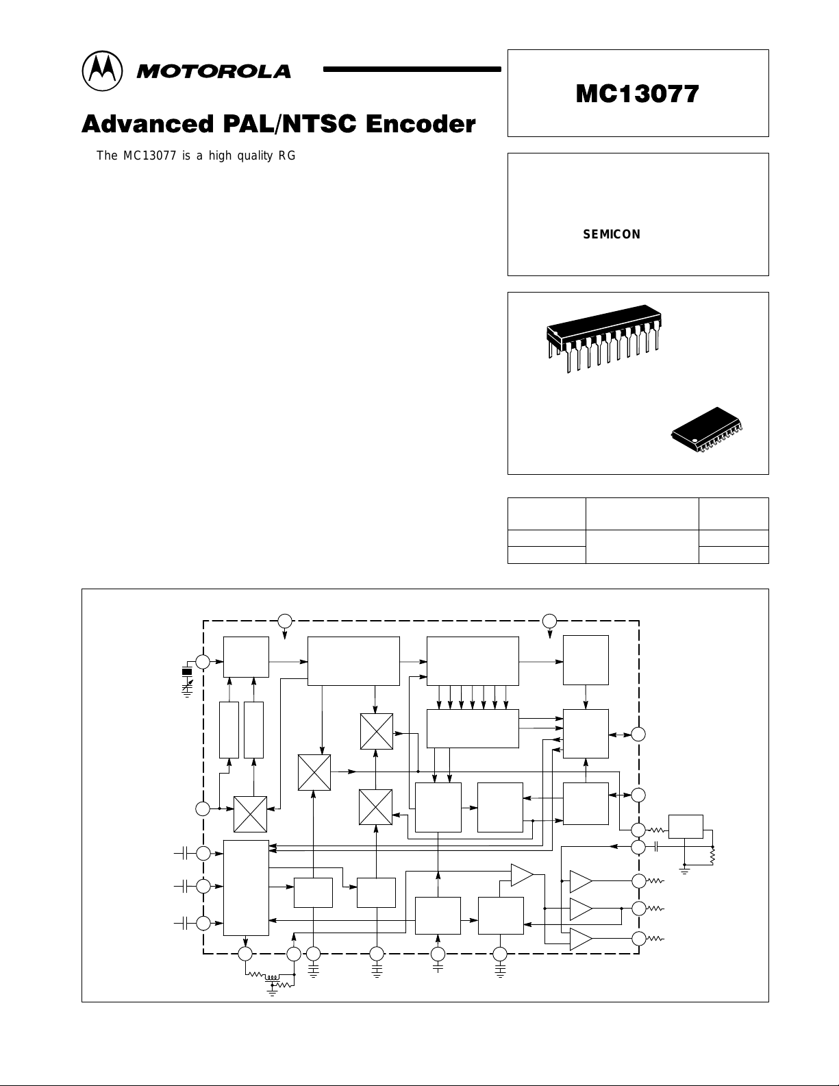
The MC13077 is a high quality RGB/YUV to NTSC/PAL encoder with
Composite Video and S–Video outputs. The IC integrates the color
difference and luma matrix circuitry, chroma modulators, subcarrier
oscillator, and logic circuitry to encode component video into a composite
video signal compatible with the NTSC/P AL standards. The IC operates off a
standard + 5.0 V supply and typically requires less than 75 mA, making it
useful in PC environments. The high degree of integration saves board
space and cost, as only passive external components are required for
operation. The IC is manufactured using Motorola’s MOSAIC process and
is available in a 20 pin DIP or SOIC package.
• Single 5.0 V Supply
• Composite Output
• S–Video Outputs
• P AL/NTSC Switchable
• P AL Squarewave Output
• P AL Sequence Resettable
• Internal/External Burst Flag
• Digitally Determined Modulator Axes
• Subcarrier Reference Drive Selectable
Order this document by MC13077/D
ADVANCED
PAL/NTSC ENCODER
SEMICONDUCTOR
TECHNICAL DATA
20
1
DW SUFFIX
PLASTIC PACKAGE
CASE 751D
(SO–20L)
PLASTIC PACKAGE
20
P SUFFIX
CASE 738
1
4x fsc Xtal/
4x fsc Input
14.32/
17.73
20 p
3.58/4.43 MHz
In/ PLL Off
Red In
1.0
µ
Green In
1.0
µ
Blue In
1.0
µ
12
13
14
V
CC
1
4x f
sc
Oscillator
8
45
PLL
LPF
Off
9
Color
Difference
Y
out
R–Y
and
B–Y
Luma
Matrix
Sync
Y
in
10 15 16
Luma Delay
1.2 k
1.2 k
°
R–Y Burst Flag
B–Y Burst Flag
B–Y
Clamp
Simplified Block Diagram
Divide by Four
Ring Counter
0
°
B–Y
Clamp
90
R–Y
Clamp
°
R–Y
Clamp
H/2
R
H
sync
Latch
Sync
Input
Divide by 512
Countdown
Decoder
H
Luma
Clamp
Sync In/
Sync Sep
MC13077DW
MC13077P
PAL
F/F
576
Luma
Clamp
ORDERING INFORMATION
Operating
Device
Gnd
11
Temperature Range
TA = 0° to +70°C
3.58/
4.43
Latch
Burst
Flag
Adjust
PAL/
NTSC
Switch
Chroma Out
Chroma In
18
19
17
20
4
3
2
Plastic DIP
Burst Flag
Out/Force Burst
Flag
PAL Squarewave
Out/ Force NTSC
Chroma
1.0 k
BPF
4.7 n
Chroma
75
S–Video
Luma
S–Video
75
Comp
Video
75
Package
SO–20L
1.1 k
MOTOROLA ANALOG IC DEVICE DATA
Motorola, Inc. 1996 Rev 2
1
Page 2
MC13077
MAXIMUM RATINGS
Rating Symbol Value Unit
Supply Voltage V
Storage Temperature T
Operating Junction Temperature T
Operating Ambient Temperature T
CC
stg
J
A
RECOMMENDED OPERATING CONDITIONS
Characteristic Min Typ Max Unit
Supply Voltage 4.5 5.0 5.5 Vdc
Sync Input Threshold Equivalent (See Figure 2) – 1.4 – Vdc
Pulse Width – 4.5 – 5.5 – µs
R, G, B Input (Amplitude for 100% Saturated Video) – 0.7 – Vpp
R–Y Input Amplitude at Pin 16 (for 100% Saturated Video) – 490 – mVpp
B–Y Input Amplitude at Pin 15 (for 100% Saturated Video) – 350 –
Y Input Amplitude (without sync) at Pins 12, 13, 14 (for 100% Saturated Video) – 700 –
Y Input Amplitude (with sync) at Delay Line – 1.0 – Vpp
External 4x Subcarrier Input to Pin 8 (If crystal is not used) – 300 – mVpp
External Subcarrier Input to Pin 9 – 0.10 to 3.0 – Vpp
Lock Range (with 4x Subcarrier Crystal specified) at Subcarrier Frequency – ± 400 – Hz
Burst Flag Input Threshold (Pin 18) – 2.5 – Vdc
NTSC/PAL Select (Pin 19) Vdc
PAL Switching Amplitude: High – 4.0 –
PAL Switching Amplitude: Low – 1.1 –
NTSC Select Threshold – 0.4 –
6.0 V
– 65 to +150 °C
+150 °C
0 to + 70 °C
ELECTRICAL CHARACTERISTICS (T
Characteristic Pin Min Typ Max Unit
Supply Current (150 Ω Load on Output Pins) 1 55 70 85 mA
Color Burst Amplitude 250 300 350 mVpp
Line–to–Line Burst Amplitude Deviation – 7.0 25 mV
Start after leading edge of Sync: NTSC (3.579 MHz)
Start after leading edge of Sync: PAL (4.43 MHz)
Duration: NTSC (3.579 MHz)
Duration: PAL (4.43 MHz)
PAL Burst Phase: Line n
PAL Burst Phase: Line n+1
NTSC Burst Phase 170 180 190
Subcarrier Leakage in Black
White (100% white)
Composite Video Output (100% saturated output)
Sync Amplitude 240 281 320 mVpp
Line–to–Line Sync Amplitude Deviation (PAL) – 7.0 – mV
Luminance Amplitude Error – – 10 %
Line–to–Line Luminance Amplitude Deviation (PAL) 2 – 3.0 – mVpp
Chrominance Amplitude Error (@ 75 Ω – – 10 %
Line–to–Line Chroma Amplitude Deviation (PAL) load) – < 14 – mVpp
Chrominance Phase Error – – 10 Degrees
Line–to–Line Chrominance Phase Error (PAL) – < 5.0 –
Black Level (RGB at Black during Blanking Intervals) – 500 – mV
Sync Tip Clamp Level above Ground 120 200 280
= 25°C, VCC = 5.0 Vdc, test circuit of Figure 1.)
A
2 & 4
(@ 75 Ω
load)
2 & 4
(@ 75 Ω
load)
–
–
–
–
125
215
–
–
5.0 to 5.3
5.4 to 5.6
9
10
135
225
–
–
–
–
–
–
145
235
25
65
Cycles
Degrees
mV
µs
2
MOTOROLA ANALOG IC DEVICE DATA
Page 3
MC13077
ELECTRICAL CHARACTERISTICS (continued) (T
= 25°C, VCC = 5.0 Vdc)
A
Characteristic Pin Min Typ Max Unit
Luma S–Video Output
Sync Amplitude 240 281 320 mVpp
Line–to–Line Sync Amplitude Deviation (PAL) 3 – 7.0 – mV
Luminance Amplitude Error (@ 75 Ω – – 10 %
Line–to–Line Luminance Amplitude Deviation (PAL) load) – 3.0 – mVpp
Black Level – 500 – mV
Sync Tip Clamp Level above Ground 120 200 280
Chroma S–Video Output
Chrominance Amplitude Error – – 10 %
Line–to–Line Chrominance Amplitude Deviation (PAL) 4 – < 14 – mVpp
Chrominance Phase Error (@ 75 Ω – – 10 Degrees
Black Level load) – 500 – mV
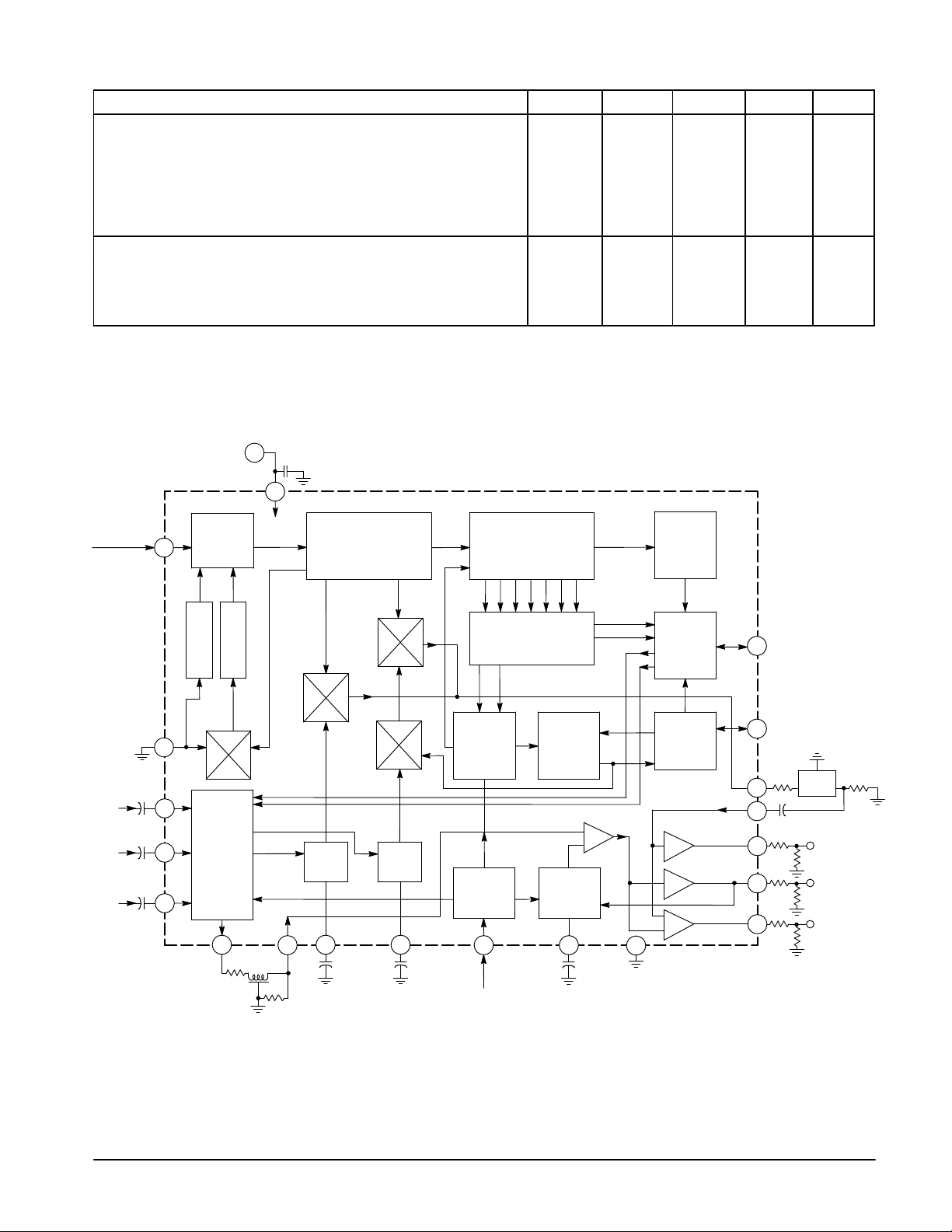
Figure 1. T est Circuit
G
1.0 µF
V
CC
1
4x Subcarrier In
1.0
µ
R
1.0
µ
G
1.0
µ
B
4x f
8
9
12
13
14
sc
Oscillator
45
°
PLL
LPF
Off
R–Y Burst Flag
B–Y Burst
Color
Difference
and
Luma
Matrix
10 15 16
Y
out
1.2 k
R–Y
B–Y
Sync
Luma Delay
1.2 k
Flag
Y
Clamp
in
Divide by Four
Ring Counter
0
°
B–Y
(B–Y) In
10 nF
90
R–Y
Clamp
°
H/2
(R–Y) In
10 nF
R
H
sync
Latch
Sync
Input
Sync In/
Sync Sep
Divide by 512
Countdown
Decoder
H
F/F PAL
Clamp
10 nF
Luma
576
Luma
Clamp
11
3.58/4.43
Switch
Ground
Latch
Burst
Flag
Adjust
PAL/
NTSC
Chroma Out
Chroma In
Burst Flag Out/
18
Force Burst Flag
PAL Squarewave
19
Out/Force NTSC
1.0 k
17
20
4
3
2
Chroma
1.0 nF
75
75
75
BPF
75
75
75
Chroma
S–Video
Luma
S–Video
Comp
Video
1.1 k
MOTOROLA ANALOG IC DEVICE DATA
3
Page 4
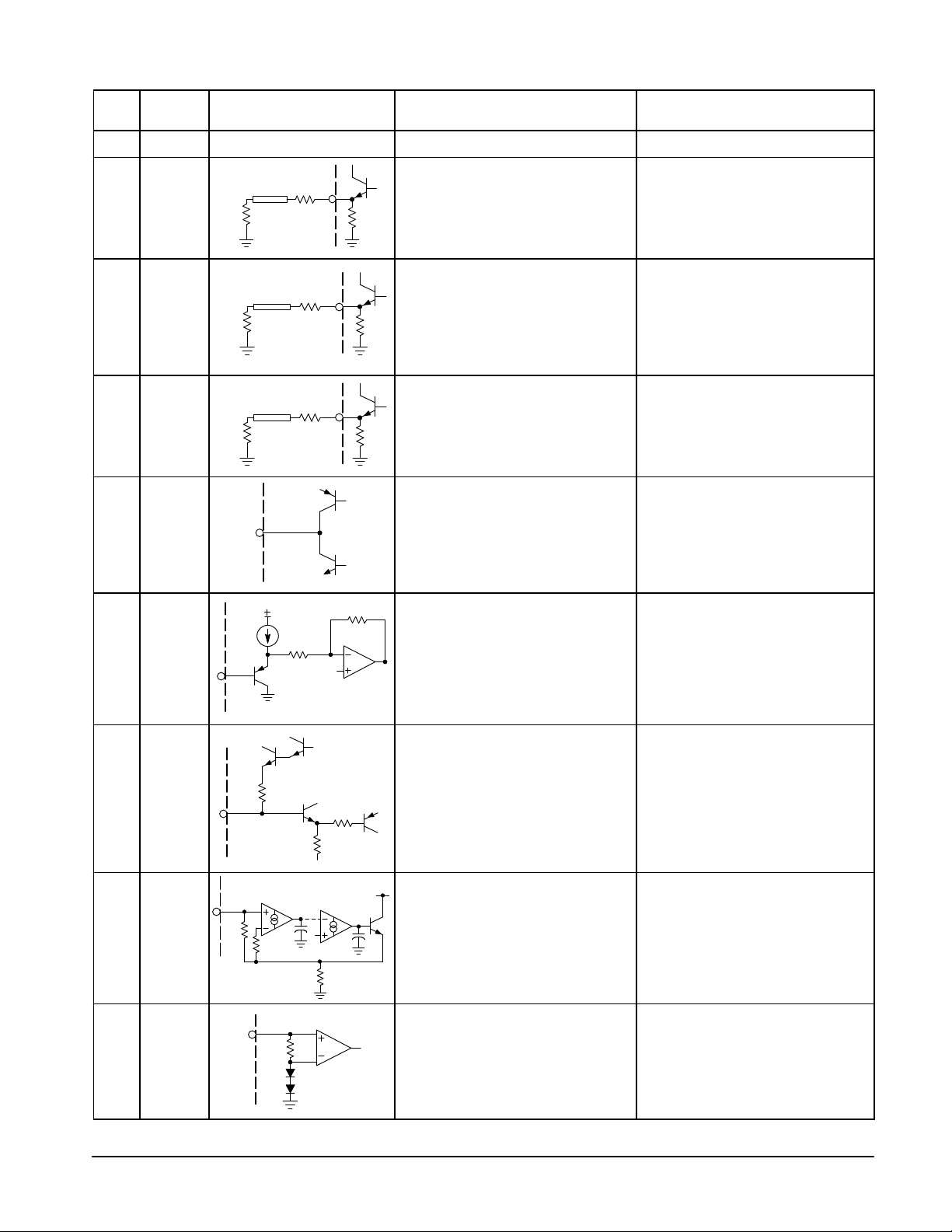
Pin Symbol
1 V
CC
2 Comp
Video
Internal Equivalent
Schematic
Zo = 75
75
Ω
Ω
75
MC13077
PIN DESCRIPTIONS
Description Expected Waveforms
Supply Voltage + 5.0 Vdc ±10%
Composite Video output. The external
75 Ω series resistor determines the
impedance of the output. The output will
Ω
1.0
drive a 75 Ω load through a 75 Ω coax.
Ω
k
1.0 Vpp (75% Color Saturation),
1.23 Vpp (100% Color Saturation) at
the 75 Ω load.
3 Luma
S–Video
4 Chroma
S–Video
5 Luma
Clamp
6 Y
In
75
75
Ω
Ω
Zo = 75
Zo = 75
Luminance S–Video output. The external
Ω
75
Ω
Ω
75
Ω
1.4 V
75 Ω series resistor determines the
impedance of the output. The output will
drive a 75 Ω load through a 75 Ω coax.
1.0
Ω
k
Chrominance S–Video output. The
external 75 Ω series resistor determines
the impedance of the output. The output
1.0
will drive a 75 Ω load through a 75 Ω
Ω
k
coax.
Luminance Output Clamp storage
capacitor. A 0.01 µF capacitor should be
connected from this pin to ground.
Luminance input from the delay line. The
delayed Luma from Pin 10 is applied at
this pin.
1.0 Vpp with sync (100% output) at the
75 Ω load.
885 mVpp (100% output) when at the
75 Ω load.
3.4 Vdc.
500 mVpp of Composite Luma when
100% saturated RGB inputs are applied.
7 Sync In/
Sync Sep
8 4x fsc Xtal
/4x fsc In
9 3.58/
4.43 MHz
In/PLL Off
4
10 k
400
10 k
gm
V
ref
2.0 V
gm
2.0 k
Composite Sync input. Negative going
sync should be applied at this pin. The
input has a threshold of 1.4 V .
V
Four times Subcarrier Frequency Crystal
CC
Oscillator pin. This pin provides for the
connection of the oscillator resonant
element. Pin may also be driven directly
with a 4x subcarrier signal.
External Subcarrier Input. This pin
provides an input to a Phase Detector and
PLL and allows phase–lock of the 4x
oscillator to an external subcarrier
reference. To disable the PLL, this pin
should be grounded. 400 Hz of pull–in and
lock–in range is possible with a crystal.
The peak voltage may not exceed VCC.
Minimum voltage should not be less than
0 V . See Figure 2 for input requirements.
300 to 600 mVpp 4x subcarrier input if
the pin is being externally driven.
Approximately 40 mVpp, if a crystal is
being used.
0.10 to 3.0 Vpp (AC coupled) of
subcarrier to phase–lock 4x oscillator or
grounded to disable the PLL.
MOTOROLA ANALOG IC DEVICE DATA
Page 5
MC13077
PIN DESCRIPTIONS (continued)
Internal Equivalent
Pin Symbol
10 Y
Out
11 Gnd Ground Ground
12 Red
13 Green
14 Blue
15 B–Y
16 R–Y
In
In
In
Clamp
Clamp
Schematic
10 k
10 k
1.4 V
20 k
V
ref
See Pin 12 Green Video input. 0.7 Vpp AC coupled (100% Color Bars).
See Pin 12 Blue Video input. 0.7 Vpp AC coupled (100% Color Bars).
Luminance Delay Line Drive Output. A
delay should be inserted between this
pin and Pin 6 to match the delay incurred
by the Chroma.
Red Video input. 0.7 Vpp AC coupled (100% Color Bars).
B–Y Clamp storage capacitor. A 0.01 µF
capacitor should be connected from this
pin to ground, unless the pin is used as
an input.
R–Y Clamp storage capacitor. A 0.01 µF
capacitor should be connected from this
pin to ground, unless the pin is used as
an input.
Description Expected Waveforms
1.0 Vpp with sync
(100% saturated Color Bar output).
If not used as an input the pin is clamped
during sync to 2.4 Vdc. Can be used as a
B–Y input (AC coupled, 350 mVpp, 100%
color saturation). Burst Flag, if disabled
at Pin 18, must be inserted here with the
following signal levels; –170 mV (NTSC),
–121 mV (PAL).
If not used as an input the pin is clamped
during sync to 2.4 Vdc. Can be used as a
R–Y input (AC coupled, 490 mVpp, 100%
color saturation). Burst Flag, if disabled
at Pin 18, must be inserted here with the
following signal level; +121 mV for PAL.
17 Chroma
Out
18 Burst Flag
Out/Force
Burst Flag
19 PAL
Square–
wave
Out/Force
NTSC
20 Chroma
In
Internal
Burst
Flag
V
CC
10 k
V
1/2 V
2.0 V
CC
10 k
CC
10 k
1.4 V
Chroma Bandpass Drive Output. 2.8 Vpp (100% Color Bars)
Burst Flag Output Disable and Force pin.
If left unconnected, internally generated
color burst will appear at Pins 2 and 4.
Burst Flag will appear at this pin (18). If
grounded, the Burst Flag will be
disabled. If externally driven from
another source of burst flag, the internal
flags will be overriden.
PAL/NTSC system switch. If grounded,
the MC13077 will encode NTSC, and if
left open, PAL.
Chroma Bandpass input. Output from
chroma bandpass filter should be
applied at this pin.
1.8 Vpp burst flag pulses if unconnected.
In PAL mode, a PAL squarewave
appears at this pin, the phase of which
can be reset by momentarily forcing the
pin to ground during the high state of
the squarewave.
1.4 Vpp (100% Color Bars) with
bandpass filter and 1.0 kΩ matching
resistors.
MOTOROLA ANALOG IC DEVICE DATA
5
Page 6

MC13077
FUNCTIONAL DESCRIPTION
Composite Sync Input
Other than the component video inputs to be encoded,
only Composite Sync is required for encoding the
components into a composite signal compatible with either
the NTSC or PAL standard. The Composite Sync input is
used internally for determining which standard to encode to,
for driving the black level clamps, and to set the timing of the
composite sync in the outputs.
The Composite Sync/Sync Separator input was designed
to accept AC or DC coupled inputs making it possible to drive
the sync input from a variety of sources. An interesting note is
that composite video can also be used for sync input. The
threshold of the sync input is 1.4 Vdc. Figure 2 shows the
requirements for sync input.
Figure 2. Sync Input Amplitude Requirements
V
CC
Baseline Voltage
Sync Tip Voltage
Sync Input
1.4 V
Gnd
Both serrated and block vertical sync can be used for
NTSC applications. PAL applications require a serrated
vertical sync. The serrations at the horizontal rate trigger the
P AL flip–flop to generate the swinging burst.
Even though the sync input of the MC13077 is well suited
for TTL interface, some functions of the IC are susceptible to
the high energy present in such signals and may be
disturbed. This disturbance may take the form of a noise
spike in the video outputs and/or a disturbance of the 4x
oscillator resulting in an incorrect encoding of the chroma
information. Therefore, it is recommended that if TTL or other
fast–edged inputs are going to be used for the sync input,
then either the amplitude and/or the edge speed of the sync
input pulse should be reduced. 300 mVpp of sync without a
reduction of edge speed has to be shown to produce
disturbance free operation. Also, a sync input of 4.0 Vpp and
edge rates of 225 ns have been shown to produce similar
results. Figure 3 shows a recommended coupling circuit for
TTL type composite sync.
Figure 3. TTL Sync Input Circuit
µ
240
0.1
7
TTL Sync
5.1 k
Luma and Color Difference Clamps
Clamping for the MC13077 occurs once every horizontal
line during sync. The absence of color creates a color
difference component voltage of zero, this null is used to
generate a reference voltage for black in the video outputs.
The clamp capacitors at Pins 5, 15 and 16 are used to store
the reference voltage during the line period.
RGB Inputs
T o encode RGB, the component video inputs (Pins 12, 13,
14) are applied to the Luma (Y) and color difference (R–Y,
B–Y) matrix. The color difference signals are then
conditioned by Sallen–key low pass filters (f–3dB = 4.0 MHz).
The inputs are designed so that 700 mVpp RGB provides
100% color saturation.
The first color difference component (R–Y) is created by
matrixing the RGB components with the following weights:
R–Y = 0.70R – 0.59G – 0.1 1B (1)
The second color difference signal (B–Y) is created in a
similar fashion by the equation:
B–Y = 0.89B – 0.59G – 0.30R (2)
These two components then receive burst flag before being
modulated by the color subcarrier to create composite
chroma.
The luma is also the result of a weighted matrixing of the
RGB components. The components and corresponding
weights are:
Y = 0.30R + 0.59G + 0.1 1B (3)
Composite sync is then added to the result of Equation 3 to
create composite luma.
The luma information thus created must be eventually
recombined with the chroma information. However, since the
chroma information created by Equations 1 and 2 is filtered
internally before being modulated then bandlimited
externally, the resultant encoded chroma experiences a
group delay that is the sum of the delay imposed by the
internal and external filtering. So, the composite luma is
output at Pin 10 so that an external delay can be inserted in
the path to match the delay incurred by the composite
chroma. The delayed composite luma is then input back into
the MC13077 at Pin 6.
Color Difference Inputs
If the MC13077 is intended to encode color difference
signals (YUV or Y, R–Y, B–Y), it becomes necessary to
bypass the color difference and luma matrix circuitry. This
can be accomplished by inputing directly to the color
modulators the color difference signals. 491 mVpp and
349 mVpp should be input to the R–Y and B–Y Clamp pins
(Pin 16 and Pin 15) respectively, to achieve 100% color
saturation in the composite video output. The luma
information can be input in two ways. The luma can be input
directly into the RGB inputs (700 mVpp without sync), or
through the delay line (1.0 Vpp with sync, sync tip–to–peak
white) in which case the RGB inputs should be cap–coupled
to ground. In either case, composite sync still needs to be
input to the MC13077 at Pin 7 (see Figures 11, 12 and 13).
If the R–Y and B–Y inputs also have burst flag, it can also
be input along with the color difference signals at these pins.
Of course, now since the color difference modulator
pre–filtering is circumvented, the delay for the luma
information should be matched only to the delay of the
bandpass filter.
6
MOTOROLA ANALOG IC DEVICE DATA
Page 7

4x f
Crystal
5–25 pF
sc
8
MC13077
9
MC13077
Figure 4. Versatility of the 4x fsc Oscillator
4x fsc Drive
Oscillator Free
Run with Crystal
(150 mV to 3.0 Vpp)
1000 pF
220
150 p
8
MC13077
9
Direct Drive of
Oscillator with
4x fsc Source
4x f
sc
Crystal
5–25 pF
f
sc
Subcarrier Reference
Input (Pull–in Range
±
of
1000 pF
400 Hz)
8
MC13077
9
Oscillator Phase Lock
with Crystal to
Subcarrier Reference
4X Subcarrier Oscillator
To encode the color difference components, an accurate
and reliable subcarrier source is required. The MC13077 has
an on–chip single pin oscillator that will free–run with a 4x f
sc
crystal, phase–lock to an external subcarrier reference with a
4x fsc crystal or resonator, or be driven externally from a 4x f
sc
source. If the 4x fsc oscillator is going to be free run, the
subcarrier input (Pin 9) should be grounded. If the 4x f
sc
oscillator is going to be phase–locked to an external
subcarrier source, the external reference should be
capacitor–coupled to Pin 9. If the 4x fsc oscillator is going to
be driven externally, Pin 8 should be driven from a network
that increases the impedance of the source at frequencies
capable of producing off–frequency oscillations. The 4x f
sc
subcarrier source, thus being defined, makes it possible to
produce accurate quadrature subcarriers for the modulators.
The 4x source is internally divided by a ring counter to
produce the quadrature subcarrier signals. These signals in
turn are provided to the color difference modulators to
produce the modulated chroma. The oscillator was designed
so that if a crystal is chosen as the resonant element of the 4x
oscillator, the crystal specifications would be common.
Crystal specifications for an adequate crystal are shown in 1
T able 1. Crystal Specifications
Frequency: 14.31818 MHz (NTSC)
Mode: Fundamental
Frequency Tolerance (@25°C), 40 ppm
Frequency Tolerance df/dfo (0° –70°C), 40 ppm
Load Capacitance: 20 pF
ESR: 50 Ω
C1(Internal Series Capacitance), 15 mpF
This crystal is a common variety and is specified as a parallel resonant.
17.734475 MHz (PAL)
Burst Flag Decoding
In order to encode to either NTSC or P AL compatibility , the
MC13077 must first determine which is the intended
standard. The MC13077 accomplishes this with an internal
decode using the sync input and the output of the divide by 4
ring counter. Internally, the Sync separator circuitry provides
an output that is sampled by the subcarrier signal from the
4x f
sc
Resonator
Subcarrier
Reference Input
1000 pF
8
MC13077
9
Oscillator Phase Lock
with Resonator to
Subcarrier Reference
ring counter. The result is an internal sync representative of
externally input sync but synchronized to the internal
subcarrier signal. This signal provides a reset for an internal
9–bit counter that provides divisions of the subcarrier signal
from the ring counter at powers of 2 (i.e. 21, 22, 23,...29 =
512). The eighth bit of the counter gives the output, fsc÷ 256.
The decision to provide burst gate timing for P AL or NTSC is
based upon the state of this output after one period of the
horizontal sync. Figure 5 shows the relationship between the
clock and the eighth bit of the counter.
Triggering of the burst PAL flip–flop due to equalizing
pulses is also inhibited by the decode circuitry. This is done
by counting out beyond a half line interval before generating
burst flag.
If the MC13077 is encoding 525/60 component video to
NTSC and the MC13077 is generating the burst flag, the start
of burst will occur 18 counts after the leading edge of sync
has been sampled, and will continue until nine cycles of burst
have occurred. Since the reset pulse of the 9–bit counter has
a resolution of 1.0/fsc, this implies that the start of burst will
occur 5.17 ± 0.1397 µs after the leading edge of sync and
also that the start (and end) of burst may differ by as much as
279.4 ns from line–to–line. If the MC13077 is encoding
625/50 to PAL, the subcarrier frequency will be
4.43361875 MHz and that implies a resolution of 225.5 ns
for the burst position. For PAL encoding, 24 counts of the
subcarrier are necessary before burst is initiated. So ten
cycles of subcarrier will occur 5.53 ± 0.1128 µs after the
leading edge of sync. After the timing of the burst gate is
selected,
the burst gate envelope is added to the color
difference components.
Another alternative to the internal determination of burst
flag is the external input of burst flag. This allows the user to
externally define the exact timing and duration of color burst.
If external burst flag is available, it can be inserted at Pin 18.
The threshold level is nominally VCC/2 and the input should
not exceed VCC. Burst will begin when the leading edge of
the burst flag input exceeds VCC/2 and will stop when it falls
below VCC/2. If it is desired to disable the burst flag, Pin 18
can be pulled low. It is also possible to insert burst flag with
the R–Y and B–Y components. This is done at the clamp pins
with the respective color difference inputs with the internal
burst flag generation disabled (Pin 18 grounded).
MOTOROLA ANALOG IC DEVICE DATA
7
Page 8

MC13077
Figure 5. Relationship Showing the Counts of a 3.58 MHz Clock
versus a 4.43 MHz Clock at the End of a Horizontal Period
f
sc
fsc/256
NTSC: (3.58 MHz) (63.56
µ
s) = 227.5 counts
Chroma Band Limiting and Luma Delay
Once the color difference and burst flag envelopes have
been modulated, the two components are internally summed
and applied to an output buffer that will drive the external
bandpass circuitry before entering the chip again at Pin 20.
The sum of the color difference modulators produces an
output that is high in harmonic content. For this reason, and
to reduce the possibility of cross color, a chroma bandpass
transformer is used to band–limit the chroma. Suggested
bandpass filters and specifications for NTSC and PAL are
shown in Figure 6a and 6b. For each of these filters,
Figure 6a. Group Delay and Magnitude
Response of the TOKO Bandpass Filter
Intended for NTSC Applications
0
Attenuation
10
20
30
ATTENUATION (dB)
40
50
RELATIVE
60
0 8.0 9.0
TOKO H286BAlS–6276DAD
NTSC Bandpass Filter
1.0 k
17
6
1.0 2.0 3.0 4.0 5.0 6.0 7.0
FREQUENCY (MHz)
4.7 nF
341
20
1.0 k
Group Delay
0.4
0.2
256 512
PAL: (4.43 MHz) (64
µ
s) = 283.75 counts
approximately 300 ns of group delay is experienced by the
filtered chroma. There is also an internal delay on the order of
100 ns due to internal filtering that must be considered. Thus
a 400 ns luma delay line is used to equalize the timing of the
luma and the chroma. Suitable 400 ns delay lines are the
TOKO H321LNP–1436PBAB and the TDK
DL122401D–1533. The delay of the luma channel is inserted
between Pins 10 and 6. Pin 10 is the buffered output of the
luma from the RGB matrix. This output is capable of driving
the external passive delay line with no external gain or
buffering required.
Figure 6b. Group Delay and Magnitude
Response of the TOKO Bandpass Filter
Intended for P AL Applications
0
Attenuation
TOKO H286BAIS–4963DAD
PAL Bandpass Filter
1.0 k
17
1.0 2.0 3.0 4.0 5.0 6.0 7.0
1
6
FREQUENCY (MHz)
4.7 nF
3
4
20
1.0 k
Group Delay
8.0
µ
GROUP DELAY ( s)
10
20
30
ATTENUATION (dB)
40
RELATIVE
50
60
0
9.0
0.4
0.2
µ
GROUP DELAY ( s)
Characteristics of TOKO Bandpass Filter
(H286BAIS – 6276DAD)
Frequency (MHz) Attenuation (dB) Group Delay (µs)
2.0 8.0 (min) 0.12
2.8 3.0 ± 3.0 0.25
3.58 Ins. Loss 3.5 (max) 0.290 ± 0.030
4.3 3.0 ± 3.0 0.24
6.2 15 (min) 0.05
8
Characteristics of TOKO Bandpass Filter
(H286BAIS – 4963DAD)
Frequency (MHz) Attenuation (dB) Group Delay (µs)
2.50 10 (min) 0.075
3.73 3.0 ± 3.0 0.24
4.43 Ins Loss 2.0 (max) 0.295 ± 0.035
5.13 3.0 ± 3.0 0.24
6.50 12 (min) 0.05
MOTOROLA ANALOG IC DEVICE DATA
Page 9

MC13077
Chroma Encoding
Modulation of the color difference components is
performed by two double–balanced mixers that are driven
from quadrature signals provided by an internal ring counter.
The quadrature signals are derived from a ring counter that is
driven by the 4x oscillator, and which makes highly accurate
quadrature angles possible.
If PAL encoding is selected, negative burst flag envelope
is provided to both B–Y and R–Y components equally, then
the R–Y envelope phase is switched positive and negative
from line–to–line to provide the PAL alternating burst phase
characteristic. An internal flip–flop that provides the internal
fH/2 switching is enabled by opening the connection at
Pin 19. If enabled, the pin will exhibit the internally generated
half line frequency squarewave. If it is desired to reverse the
sense of the P AL swinging burst, it can be done at this pin by
pulling Pin 19 low when the squarewave is high. The
component envelopes with the proper PAL burst phase are
then modulated to produce the composite chroma.
If the MC13077 is encoding to NTSC, only the B–Y color
difference component is provided a negative burst flag. This
envelope when modulated results in the characteristic –180°
phase difference between the color burst and the subcarrier
for the B–Y component. Pin 19 should be grounded for NTSC
operation to disable the PAL flip–flop.
Video Outputs
After being filtered, the composite chroma is recombined
with the composite luma information for the Composite Video
output. The composite chroma and composite luma
components are also kept separate and buffered for the
chroma S–Video and luma S–Video outputs. The video
outputs are provided with low impedance emitter–follower
stages and, therefore, require an external 75 Ω impedance
determining series resistor (see Figure 7). The outputs are
designed to drive a 75 Ω load through the external 75 Ω
series resistor.
The Composite Video output will provide 1.23 Vpp of video
(sync tip–to–peak chroma) for 100% saturated video at the
75 Ω load. Luma S–Video will be 1.0 Vpp (sync tip–to–peak
white) at the 75 Ω load and the Chroma S–Video output will
provide 885 mVpp at the 75 Ω load.
Figure 7. Composite S–Luma and
S–Chroma Video Outputs
MC13077
75
1.0 k
Ω
Ω
Zo = 75
Ω
75
Ω
APPLICATIONS INFORMATION
Figures 8 through 13 are application examples showing
the versatility of the MC13077.
Figure 8. Standard Encoder Application with RGB Inputs and Phase–Locked Subcarrier
Chroma
Bandpass
1.1 k
4.7 n
PAL/NTSC
Burst Flag
75 75 75
S-Luma
Comp. Video
+5.0 V
1.0
Chroma In
20
µ
F
CC
V
1.0
k
Chroma Out
(R-Y) Clamp
S-Chroma
Luma Clamp
(B-Y) Clamp
MC13077
Luma In
10 n
10 n10 n
1.0
B-In
14.32/
17.73
Sync In
µ
20 p
1.0
G-In
µ
1.0
R-In
1.0 n
Subcarrier In
µ
Gnd
111213141516171819
10987654321
Luma Out
1.2 k
MOTOROLA ANALOG IC DEVICE DATA
Luma Delay
1.2 k
9
Page 10

1.1 k
+5.0 V
MC13077
Figure 9. Encoder with RGB Inputs and Unlocked Subcarrier
Chroma
Bandpass
1.0
4.7 n
Chroma In
20
PAL/NTSC
Burst Flag
k
Chroma Out
(R-Y) Clamp
(B-Y) Clamp
MC13077
10 n10 n
B-In
1.0
1.0
µ
µ
G-In
R-In
1.0
µ
Gnd
111213141516171819
10987654321
1.1 k
1.2 k
14.32/
17.73
Sync In
20 p
Luma Delay
1.0
µ
F
CC
V
75 75 75
S-Luma
Comp. Video
S-Chroma
Luma Clamp
10 n
Luma In
Figure 10. Encoder with RGB Inputs and 4x Subcarrier Drive
Chroma
Bandpass
1.0
4.7 n
Chroma In
20
PAL/NTSC
Burst Flag
k
Chroma Out
(R-Y) Clamp
(B-Y) Clamp
MC13077
1.0
B-In
µ
G-In
10 n10 n
1.0
1.2 k
Luma Out
µ
µ
1.0
R-In
Gnd
111213141516171819
10
+5.0 V
1.0
10987654321
µ
F
CC
V
75 75 75
S-Luma
Comp. Video
S-Chroma
Luma Clamp
10 n
Luma In
1.2 k
Sync In
150 p
220
1.0 n
4X Subcarrier In
Luma Delay
1.2 k
Luma Out
MOTOROLA ANALOG IC DEVICE DATA
Page 11

1.1 k
+5.0 V
MC13077
Figure 11. Encoder with Luma and Color Difference Inputs
Using Phase–Locked Subcarrier
R–Y, B–Y Source
1.0
k
(R-Y) Clamp
Luma Clamp
Impedance
Ω
<500
(B-Y) Clamp
MC13077
Luma In
10 n
10 n10 n
14.32/
17.73
Sync In
20 p
1.0
4.7 n
Chroma In
20
µ
F
CC
V
Chroma
Bandpass
PAL/NTSC
Burst Flag
75 75 75
S-Luma
Comp. Video
Chroma Out
S-Chroma
Y-In
4.7
µ
Gnd
111213141516171819
10987654321
1.0 n
Subcarrier In
Luma Out
1.2 k
Luma Delay
1.2 k
Figure 12. Encoder with Composite Luma and Color Difference Inputs
Using Phase–Locked Subcarrier
R–Y, B–Y Source
1.1 k
+5.0 V
1.0
4.7 n
Chroma In
20
µ
F
CC
V
Chroma
Bandpass
PAL/NTSC
Burst Flag
75 75 75
S-Luma
Comp. Video
Chroma Out
S-Chroma
1.0
k
(R-Y) Clamp
Luma Clamp
Impedance
Ω
<500
(B-Y) Clamp
MC13077
Luma In
10 n
10 n10 n
14.32/
17.73
Sync In
1.0 n
20 p
Gnd
111213141516171819
10987654321
1.0 n
Subcarrier In
MOTOROLA ANALOG IC DEVICE DATA
1.2 k
Luma Delay
1.2 k
Composite
Y–Input
11
Page 12

MC13077
Figure 13. Encoder with Composite Luma and Color Difference Inputs
Using the Sync Separator and Having Phase–Locked Subcarrier
R–Y, B–Y Source
1.1 k
+5.0 V
1.0
4.7 n
Chroma In
20
µ
F
CC
V
Chroma
Bandpass
PAL/NTSC
Burst Flag
75 75 75
S-Luma
Comp. Video
Chroma Out
S-Chroma
1.0
k
(R-Y) Clamp
Luma Clamp
Impedance
Ω
<500
(B-Y) Clamp
MC13077
Luma In
10 n
10 n10n
14.32/
17.73
Sync In
10 n
1.0 n
20 p
Gnd
111213141516171819
10987654321
1.0 n
Subcarrier In
Recommended Vendors
Bandpass Filters
and Delay Lines
TOKO America Inc.
1250 Feehanville Drive
Mt. Prospect, IL 60056
(708) 297–0070
(708) 699–7864 (fax)
Delay Lines
TDK Corp. of America
1600 Feehanville Drive
Mt. Prospect, IL 60056
(708) 803–6100
Luma Delay
1.2 k
1.2 k
Crystals
Fox Electronics
5570 Enterprise Pkwy
Ft. Myers, FL 33905
(813) 693–0099
Standard Crystal Corporation
9940 E. Baldwin Place
El Monte, CA 91731
(818) 443–2121
Composite
Y–Input
12
MOTOROLA ANALOG IC DEVICE DATA
Page 13

MC13077
OUTLINE DIMENSIONS
P SUFFIX
PLASTIC PACKAGE
CASE 738–03
ISSUE E
-T-
SEATING
PLANE
-A-
1120
B
110
C
K
E
N
GF
D
20 PL
0.25 (0.010) T A
M M
PLASTIC PACKAGE
–A–
20
11
–B–
P10X
0.010 (0.25)
1
10
D20X
0.010 (0.25) B
M
S
A
T
S
C
SEATING
–T–
18X
G
K
PLANE
L
J 20 PL
DW SUFFIX
CASE 751D–04
(SO–20L)
ISSUE E
M
M
B
J
F
M
M
R
X 45
M M
_
0.25 (0.010) T B
NOTES:
1. DIMENSIONING AND TOLERANCING PER ANSI
Y14.5M, 1982.
2. CONTROLLING DIMENSION: INCH.
3. DIMENSION L TO CENTER OF LEAD WHEN
FORMED PARALLEL.
4. DIMENSION B DOES NOT INCLUDE MOLD
FLASH.
INCHES MILLIMETERS
MIN MINMAX MAX
DIM
A
B
C
D
E
F
G
J
K
L
M
N
NOTES:
1. DIMENSIONING AND TOLERANCING PER
ANSI Y14.5M, 1982.
2. CONTROLLING DIMENSION: MILLIMETER.
3. DIMENSIONS A AND B DO NOT INCLUDE
MOLD PROTRUSION.
4. MAXIMUM MOLD PROTRUSION 0.150
(0.006) PER SIDE.
5. DIMENSION D DOES NOT INCLUDE
DAMBAR PROTRUSION. ALLOWABLE
DAMBAR PROTRUSION SHALL BE 0.13
(0.005) TOTAL IN EXCESS OF D DIMENSION
AT MAXIMUM MATERIAL CONDITION.
DIM MIN MAX MIN MAX
A 12.65 12.95 0.499 0.510
B 7.40 7.60 0.292 0.299
C 2.35 2.65 0.093 0.104
D 0.35 0.49 0.014 0.019
F 0.50 0.90 0.020 0.035
G 1.27 BSC 0.050 BSC
J 0.25 0.32 0.010 0.012
K 0.10 0.25 0.004 0.009
M 0 7 0 7
P 10.05 10.55 0.395 0.415
R 0.25 0.75 0.010 0.029
1.070
1.010
0.260
0.240
0.180
0.150
0.022
0.015
0.050 BSC
0.070
0.050
0.100 BSC
0.015
0.008
0.140
0.110
0.300 BSC
°
°
15
0
0.040
0.020
__
25.66
6.10
3.81
0.39
1.27 BSC
1.27
2.54 BSC
0.21
2.80
7.62 BSC
°
0
0.51
INCHESMILLIMETERS
__
27.17
6.60
4.57
0.55
1.77
0.38
3.55
°
15
1.01
MOTOROLA ANALOG IC DEVICE DATA
13
Page 14

MC13077
Motorola reserves the right to make changes without further notice to any products herein. Motorola makes no warranty , representation or guarantee regarding
the suitability of its products for any particular purpose, nor does Motorola assume any liability arising out of the application or use of any product or circuit, and
specifically disclaims any and all liability, including without limitation consequential or incidental damages. “T ypical” parameters which may be provided in Motorola
data sheets and/or specifications can and do vary in different applications and actual performance may vary over time. All operating parameters, including “Typicals”
must be validated for each customer application by customer’s technical experts. Motorola does not convey any license under its patent rights nor the rights of
others. Motorola products are not designed, intended, or authorized for use as components in systems intended for surgical implant into the body, or other
applications intended to support or sustain life, or for any other application in which the failure of the Motorola product could create a situation where personal injury
or death may occur. Should Buyer purchase or use Motorola products for any such unintended or unauthorized application, Buyer shall indemnify and hold Motorola
and its officers, employees, subsidiaries, affiliates, and distributors harmless against all claims, costs, damages, and expenses, and reasonable attorney fees
arising out of, directly or indirectly, any claim of personal injury or death associated with such unintended or unauthorized use, even if such claim alleges that
Motorola was negligent regarding the design or manufacture of the part. Motorola and are registered trademarks of Motorola, Inc. Motorola, Inc. is an Equal
Opportunity/Affirmative Action Employer.
How to reach us:
USA/EUROPE /Locations Not Listed: Motorola Literature Distribution; JAPAN: Nippon Motorola Ltd.: SPD, Strategic Planning Office, 4–32–1,
P.O. Box 5405, Denver, Colorado 80217. 303–675–2140 or 1–800–441–2447 Nishi–Gotanda, Shinagawa–ku, Tokyo 141, Japan. 81–3–5487–8488
Mfax: RMFAX0@email.sps.mot.com – TOUCHTONE 602–244–6609 ASIA/PACIFIC: Motorola Semiconductors H.K. Ltd.; 8B Tai Ping Industrial Park,
INTERNET: http://motorola.com/sps
14
– US & Canada ONLY 1–800–774–1848 51 Ting Kok Road, T ai Po, N.T., Hong Kong. 852–26629298
◊
MOTOROLA ANALOG IC DEVICE DATA
Mfax is a trademark of Motorola, Inc.
MC13077/D
 Loading...