

Page 1
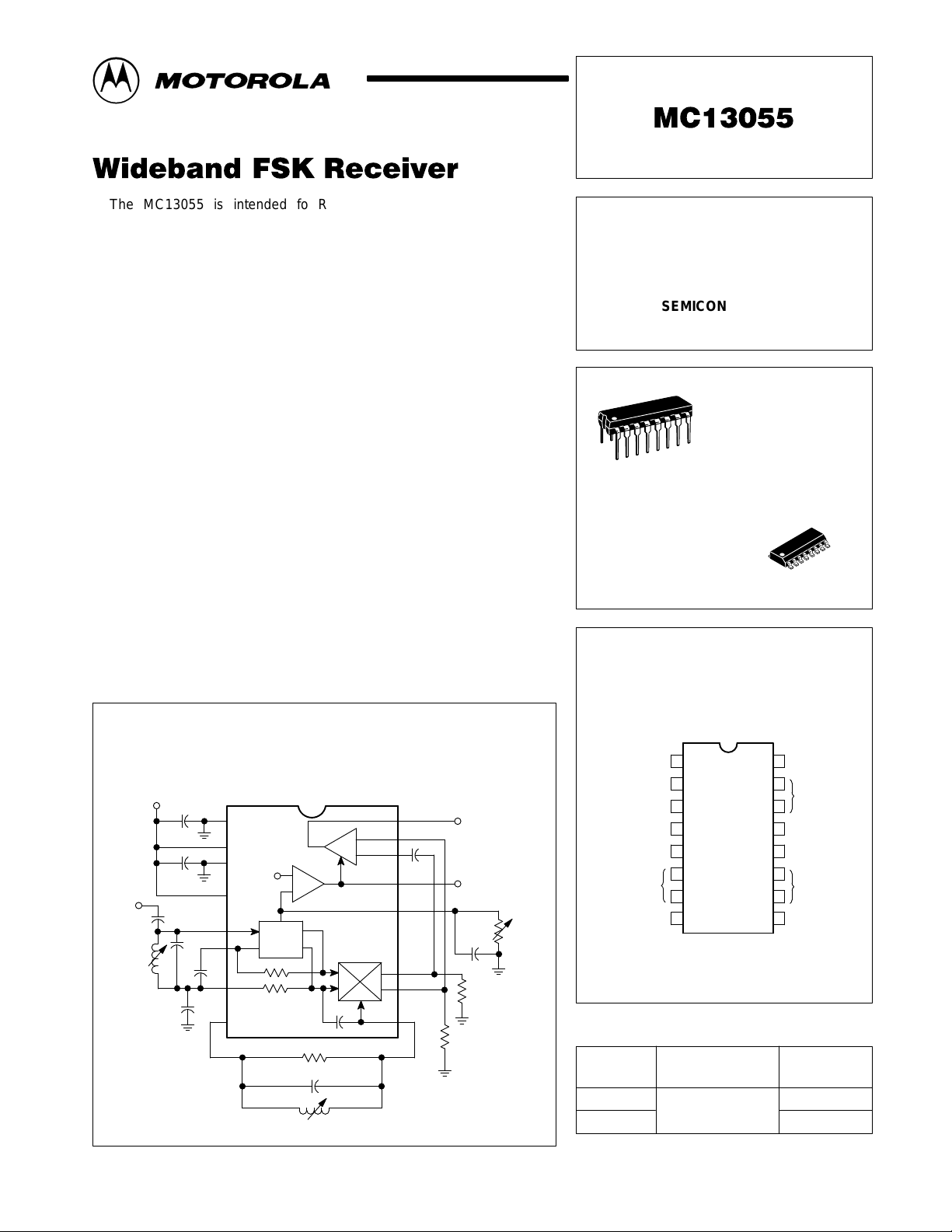
The MC13055 is intended fo RF data link systems using carrier
frequencies up to 40 MHz and FSK (frequency shift keying) data rates up to
2.0 M Baud (1.0 MHz). This design is similar to the MC3356, except that it
does not include the oscillator/mixer. The IF bandwidth has been increased
and the detector output has been revised to a balanced configuration. The
received signal strength metering circuit has been retained, as has the
versatile data slicer/comparator.
• Input Sensitivity 20 µV @ 40 MHz
• Signal Strength Indicator Linear Over 3 Decades
• Available in Surface Mount Package
• Easy Application, Few Peripheral Components
Order this document by MC13055/D
WIDEBAND
FSK
RECEIVER
SEMICONDUCTOR
TECHNICAL DATA
P SUFFIX
PLASTIC PACKAGE
CASE 648
40MHz
IF
Input
Ω
)
(50
Figure 1. Block Diagram and Application Circuit
V
CC
L1
22pF
0.01
0.01
0.01
27pF
0.1
1
2
3
0.8V
4
5
6
7
V
8
CC
–
+
Limiter
1.0k
39pF
L2
16
15
+
14
–
100pF
13
12
11
10
9
Data
Output
Carrier
Detect
68pF
3.9k
5.0k
3.9k
Squelch
Adjust
(meter)
D SUFFIX
PLASTIC PACKAGE
CASE 751B
(SO–16)
PIN CONNECTIONS
Comparator Gnd
Comparator V
CC
IF Ground
IF V
CC
Limiter Input
Limiter Bias
Quad Bias
ORDERING INFORMATION
Device
MC13055D
MC13055P
Temperature Range
1
2
3
4
5
6
7
8
Operating
TA = – 40 to +85°C
16
Data Out
+
15
Comparator
–
14
13
Carrier Detect
12
Meter Drive
11
Detector
10
Out
9
Quad Input
Package
Plastic DIP
SO–16
MOTOROLA ANALOG IC DEVICE DATA
Motorola, Inc. 1996 Rev 2
1
Page 2
MC13055
MAXIMUM RATINGS
Rating Symbol Value Unit
Power Supply Voltage V
Operating Supply Voltage Range V2, V4 3.0 to 12 Vdc
Junction Temperature T
Operating Ambient Temperature Range T
Storage Temperature Range T
Power Dissipation, Package Rating P
CC(max)
J
A
stg
D
15 Vdc
150 °C
–40 to +85 °C
–65 to +150 °C
1.25 W
ELECTRICAL CHARACTERISTICS (V
Characteristic Conditions Min Typ Max Unit
Total Drain Current 12 + 14 – 20 25 mA
Data Comparator Pull–Down Current I16 – 10 – mA
Meter Drive Slope versus Input I12 4.5 7.0 9.0 µA/dB
Carrier Detect Pull–Down Current I13 – 1.3 – mA
Carrier Detect Pull–Up Current I13 – 500 – µA
Carrier Detect Threshold Voltage V12 690 800 1010 mV
DC Output Current I10, I11 – 430 – µA
Recovered Signal V10 – V11 – 350 – mVrms
Sensitivity for 20 dB S + N/N, BW = 5.0 MHz VIN – 20 – µVrms
S + N/N at Vin = 50 µV V10 – V11 – 30 – dB
Input Impedance @ 40 MHz R
Quadrature Coil Loading R
= 5.0 Vdc, fo = 40 MHz, f
CC
Pin 5, Ground –
in
C
in
in
C
in
= 1.0 MHz, ∆f = ±1.0 MHz, TA = 25°C, test circuit of Figure 2.)
mod
Pin 9 to 8 –
–
–
4.2
4.5
7.6
5.2
–
–
–
–
Figure 2. T est Circuit
1
16
kΩ
pF
kΩ
pF
Input
V
CC
22pF
L1
0.01
0.01
27pF
0.010.01
0.1
2
3
4
5
6
7
8
1.0k
39pF
L2
2
15
14
13
12
11
10
100pF
Carrier
Detect Output
Meter Drive
Detector
Output
9
3.9k3.9k
Coils – Shielded
Coilcraft UNI–10/142
L1 Gray 8–1/2 Turns, nominal 300 nH
L2 Black 10–1/2 Turns, nominal 380 nH
MOTOROLA ANALOG IC DEVICE DATA
Page 3
MC13055
Figure 3. Overall Gain, Noise, AM Rejection Figure 4. Meter Current versus Signal
0
Output f
–10
mod
∆
f = 1.0 MHz
–20
–30
Noise
–40
–50
AMR 1.0 kHz
30%
RELATIVE OUTPUT (dB)
–60
–100
SIGNAL INPUT (dBm)
Figure 5. Untuned Input: Limiting Sensitivity
versus Frequency
–10
–20
–30
–40
–50
–60
–70
–80
, INPUT LIMITING SENSITIVITY (dBm)
–90
IN
V
–100
0
Input
10
0.1
0.1
5
51
7
MC13055
9
20k
8
f, INPUT FREQUENCY (MHz)
= 1.0 MHz
µ
600
500
400
VCC = 5.0 V, 7.0 V
3.0 V
12 V
300
200
l12, METER CURRENT ( A)
100
0–20–60 –40–80
0
–100
0–20–40–60–80
INPUT SIGNAL (dBm)
Figure 6. Untuned Input: Meter Current
versus Frequency
800
Input 0 dBm
700
–10
µ
600
–20
500
–30
–40
400
–50
300
–60
200
–70
l12, METER CURRENT ( Adc)
100
–80
0
10090807060504030200
f, INPUT FREQUENCY (MHz)
Input
0.1
0.1
MC13055
9
20k
8
5
51
7
1009080706050403020100
Figure 7. Limiting Sensitivity and Detuning
versus Supply V oltage
–40
–50
–60
–70
–80
, INPUT LIMITING SENSITIVITY (dBm)
–90
IN
V
40 MHz
Limiting
Sensitivity
VCC, SUPPLY VOLTAGE (Vdc)
Quadrature
Coil Tuning
119.05.0 7.03.00
MOTOROLA ANALOG IC DEVICE DATA
Figure 8. Detector Current and Power Supply
Current versus Supply Voltage
40 3
40.2
40.1
40.0
39.9
1200
µ
1000 50
I10 + I11
800
39.8
l10 + l11, DETECTOR CURRENT ( Adc)
600
400
200
I2 + I4
0
1.0
7.05.03.00
39.7
39.6
39.5
39.4
QUAD COIL TUNING (MHz)
39.3
39.2
15
131.0
VCC, SUPPLY VOLTAGE (Vdc)
60
40
30
20
10
l2 + I4, POWER SUPPLY CURRENT (mA)
0
13 15119.0
3
Page 4

MC13055
Figure 10. Carrier Detect Threshold versus
Figure 9. Recovered Audio versus T emperature
1000
4.0
2.0
–2.0
–4.0
–6.0
–8.0
–10
–12
V10, RELATIVE AUDIO OUTPUT (dB)
0
–60
TA, AMBIENT TEMPERATURE (
140120100806040200–20–40
°
C)
900
800
700
600
V12, CARRIER DETECT THRESHOLD (mV)
500
–60
Figure 11. Meter Current versus Temperature Figure 12. Input Limiting versus Temperature
µ
l12, METER CURRENT ( A)
600
500
400
300
200
100
–60
–10
–40
Input 0 dBm
–20
–30
–40
–50
–60
TA, AMBIENT TEMPERATURE (
–50
–60
–70
–80
, INPUT LIMITING SENSITIVITY (dBm)
–90
IN
V
140120100806040200–20
°
C)
–60
T emperature
TA, AMBIENT TEMPERATURE (
TA, AMBIENT TEMPERATURE (
140120100806040200–20–40
°
C)
140120100806040200–20–40
°
C)
Figure 13. Input Impedance, Pin 5
1.0
Cp = 4p5
0.5
0.2
0
200M
0.2
100M
0.5
0.5
50M
Rp = 4k2
Y = 0.24 + j1.1
2.01.00.2
20M
30M
2.0
10M
5.0
1.0M
5.0
1.0
4
MOTOROLA ANALOG IC DEVICE DATA
Page 5

BNC
MC13055
Figure 14. T est Fixture
(Component Layout)
.01
22P
.01
.3
µ
H
.1
27P
.01
.01
.4 µH
MC13055
1K
39P
100P
3.9K
68P
3.9K
5K
POT
4
I
CARRIER
DETECT
METER
DRIVE
DETECTOR OUTPUT
SQUELCH
CONTROL
4
I
(Circuit Side View)
DATA OUT
MC13055
GND VCC
INPUT
4
I
MOTOROLA ANALOG IC DEVICE DATA
4
I
5
Page 6

MC13055
47
2
80
76
16
74
78 79
77
94
85
92
92
89
13
91
86
14
90
87
84
83
82
81
1
48
39
38
10
11
30
29
28
27
45
15
37
8
9
36
33 34
31 32
35
26
25
46
65
49
50
51
53
52
73
Figure 15. Internal Schematic
72
71
Figure 15. d
69
70
67
66
12
68
25
26
60 61 62 63 64
58 57 56 55 54
BB
13 14 15 16 17 18 19 20 21 22 23 24
4
5
6
7
59
3
6
MOTOROLA ANALOG IC DEVICE DATA
Page 7

MC13055
GENERAL DESCRIPTION
The MC13055 is an extended frequency range FM IF,
quadrature detector, signal strength detector and data
shaper. It is intended primarily for FSK data systems. The
design is very similar to MC3356 except that the
oscillator/mixer has been removed, and the frequency
capability of the IF has been raised about 2:1. The detector
output configuration has been changed to a balanced,
open–collector type to permit symmetrical drive of the data
shaper (comparator). Meter drive and squelch features have
been retained.
The limiting IF is a high frequency type, capable of being
operated up to 100 MHz. It is expected to be used at 40 MHz
in most cases. The quadrature detector is internally coupled
to the IF, and a 2.0 pF quadrature capacitor is internally
provided. The 20 dB quieting sensitivity is approximately
20 µV, tuned input, and the IF can accept signals up to
220 mVrms without distortion or change of detector
quiescent DC level.
The IF is unusual in that each of the last 5 stages of the
6 stage limiter contains a signal strength sensitive, current
sinking device. These are parallel connected and buffered
to produce a signal strength meter drive which is fairly linear
for IF input signals of 20 µV to 20 mVrms (see Figure 4).
A simple squelch arrangement is provided whereby the
meter current flowing through the meter load resistance flips
a comparator at about 0.8 Vdc above ground. The signal
strength at which this occurs can be adjusted by changing
the meter load resistor. The comparator (+) input and output
are available to permit control of hysteresis. Good positive
action can be obtained for IF input signals of above
20 µVrms. A resistor (R) from Pin 13 to Pin 12 will provide
VCC/R of feedback current. This current can be correlated to
an amount of signal strength hysteresis by using Figure 4.
The squelch is internally connected to the data shaper.
Squelch causes the data shaper to produce a high (V
output.
The data shaper is a complete “floating” comparator, with
diodes across its inputs. The outputs of the quadrature
detector can be fed directly to either or preferably both inputs
of the comparator to produce a squared output swinging from
VCC to ground in inverted or noninverted form.
CC)
MOTOROLA ANALOG IC DEVICE DATA
7
Page 8

–T–
OUTLINE DIMENSIONS
PLASTIC PACKAGE
–A–
916
B
18
F
H
G
D
16 PL
0.25 (0.010) T
–A–
16 9
18
G
SEATING
PLANE
D
16 PL
0.25 (0.010) A
M
T
C
S
SEATING
–T–
PLANE
K
M
M
A
PLASTIC PACKAGE
CASE 751B–05
–B–
8 PLP
0.25 (0.010) B
K
C
M
S
B
S
MC13055
P SUFFIX
CASE 648–08
ISSUE R
L
J
D SUFFIX
(SO–16)
ISSUE J
M
S
R
X 45
NOTES:
1. DIMENSIONING AND TOLERANCING PER ANSI
Y14.5M, 1982.
2. CONTROLLING DIMENSION: INCH.
3. DIMENSION L TO CENTER OF LEADS WHEN
FORMED PARALLEL.
4. DIMENSION B DOES NOT INCLUDE MOLD FLASH.
5. ROUNDED CORNERS OPTIONAL.
DIM MIN MAX MIN MAX
A 0.740 0.770 18.80 19.55
B 0.250 0.270 6.35 6.85
C 0.145 0.175 3.69 4.44
D 0.015 0.021 0.39 0.53
F 0.040 0.70 1.02 1.77
G 0.100 BSC 2.54 BSC
M
_
F
J
H 0.050 BSC 1.27 BSC
J 0.008 0.015 0.21 0.38
K 0.110 0.130 2.80 3.30
L 0.295 0.305 7.50 7.74
M 0 10 0 10
S 0.020 0.040 0.51 1.01
NOTES:
1. DIMENSIONING AND TOLERANCING PER ANSI
Y14.5M, 1982.
2. CONTROLLING DIMENSION: MILLIMETER.
3. DIMENSIONS A AND B DO NOT INCLUDE
MOLD PROTRUSION.
4. MAXIMUM MOLD PROTRUSION 0.15 (0.006)
PER SIDE.
5. DIMENSION D DOES NOT INCLUDE DAMBAR
PROTRUSION. ALLOWABLE DAMBAR
PROTRUSION SHALL BE 0.127 (0.005) TOTAL
IN EXCESS OF THE D DIMENSION AT
MAXIMUM MATERIAL CONDITION.
DIM MIN MAX MIN MAX
A 9.80 10.00 0.386 0.393
B 3.80 4.00 0.150 0.157
C 1.35 1.75 0.054 0.068
D 0.35 0.49 0.014 0.019
F 0.40 1.25 0.016 0.049
G 1.27 BSC 0.050 BSC
J 0.19 0.25 0.008 0.009
K 0.10 0.25 0.004 0.009
M 0 7 0 7
____
P 5.80 6.20 0.229 0.244
R 0.25 0.50 0.010 0.019
MILLIMETERSINCHES
____
INCHESMILLIMETERS
Motorola reserves the right to make changes without further notice to any products herein. Motorola makes no warranty , representation or guarantee regarding
the suitability of its products for any particular purpose, nor does Motorola assume any liability arising out of the application or use of any product or circuit, and
specifically disclaims any and all liability, including without limitation consequential or incidental damages. “T ypical” parameters which may be provided in Motorola
data sheets and/or specifications can and do vary in different applications and actual performance may vary over time. All operating parameters, including “Typicals”
must be validated for each customer application by customer’s technical experts. Motorola does not convey any license under its patent rights nor the rights of
others. Motorola products are not designed, intended, or authorized for use as components in systems intended for surgical implant into the body, or other
applications intended to support or sustain life, or for any other application in which the failure of the Motorola product could create a situation where personal injury
or death may occur. Should Buyer purchase or use Motorola products for any such unintended or unauthorized application, Buyer shall indemnify and hold Motorola
and its officers, employees, subsidiaries, affiliates, and distributors harmless against all claims, costs, damages, and expenses, and reasonable attorney fees
arising out of, directly or indirectly, any claim of personal injury or death associated with such unintended or unauthorized use, even if such claim alleges that
Motorola was negligent regarding the design or manufacture of the part. Motorola and are registered trademarks of Motorola, Inc. Motorola, Inc. is an Equal
Opportunity/Affirmative Action Employer.
Mfax is a trademark of Motorola, Inc.
How to reach us:
USA/EUROPE/ Locations Not Listed: Motorola Literature Distribution; JAPAN: Nippon Motorola Ltd.: SPD, Strategic Planning Office, 4–32–1,
P.O. Box 5405, Denver, Colorado 80217. 303–675–2140 or 1–800–441–2447 Nishi–Gotanda, Shinagawa–ku, Tokyo 141, Japan. 81–3–5487–8488
Mfax: RMFAX0@email.sps.mot.com – TOUCHTONE 602–244–6609 ASIA/PACIFIC: Motorola Semiconductors H.K. Ltd.; 8B Tai Ping Industrial Park,
– US & Canada ONLY 1–800–774–1848 51 Ting Kok Road, T ai Po, N.T., Hong Kong. 852–26629298
INTERNET: http://motorola.com/sps
8
◊
MOTOROLA ANALOG IC DEVICE DATA
MC13055/D
 Loading...