

Page 1
Device
Operating
Temperature Range
Package
SEMICONDUCTOR
TECHNICAL DATA
DUAL CONVERSION
AM RECEIVER
ORDERING INFORMATION
MC13030DW TA = –40° to +85°C SOIC–28
DW SUFFIX
PLASTIC PACKAGE
CASE 751F
28
1
(Top View)
PIN CONNECTIONS
Order this document by MC13030/D
1
2
3
4
5
6
7
8
9
10
11
12
13
14
28
27
26
25
24
23
22
21
20
19
18
17
16
15
Mix1 In
Mix1 In
RF Gnd
FET RF AGC
RF AGC2
RF AGC Adj
Mix1 RF AGC Adj
SD Level
IF Gnd
SD IF Out
S Level Out
IF AGC In
AF Out
V
CC
VCO Out
VCO
VCO Ref
Mix1 Out
Mix1 Out
V
ref
Mix2 In
Mix2 Out
Mix2 Out
Xtal Osc E
Xtal Osc B
IF In
Det V
ref
Det In
1
MOTOROLA ANALOG IC DEVICE DATA
The MC13030 is a dual conversion AM receiver designed for car radio
applications. It includes a high dynamic range first mixer, local oscillator,
second mixer and second oscillator, and a high gain AGC’d IF and
detector. Also included is a signal strength output, two delayed RF AGC
outputs for a cascode FET/bipolar RF amplifier and diode attenuator, a
buffered IF output stage and a first local oscillator output buf fer for driving
a synthesizer . Frequency range of the first mixer and oscillator is 100 kHz
to 50 MHz.
Applications include single band and multi–band car radio receivers, and
shortwave receivers.
• Operation from 7.5 to 9.0 Vdc
• First Mixer, 3rd Order Intercept = 20 dBm
• Buffered First Oscillator Output
• Second Mixer, 3rd Order Intercept = +5.0 dBm
• No Internal Beats Between 1st and 2nd Oscillator Harmonics
• Signal Strength Output
• Limited 2nd IF Output for Frequency Counter Station Detector
• Adjustable IF Output Station Detector Level
• Adjustable RF AGC Threshold for Both Mixer Inputs
• Two Delayed AGC Outputs for Cascode RF Stage and Diode Attenuator
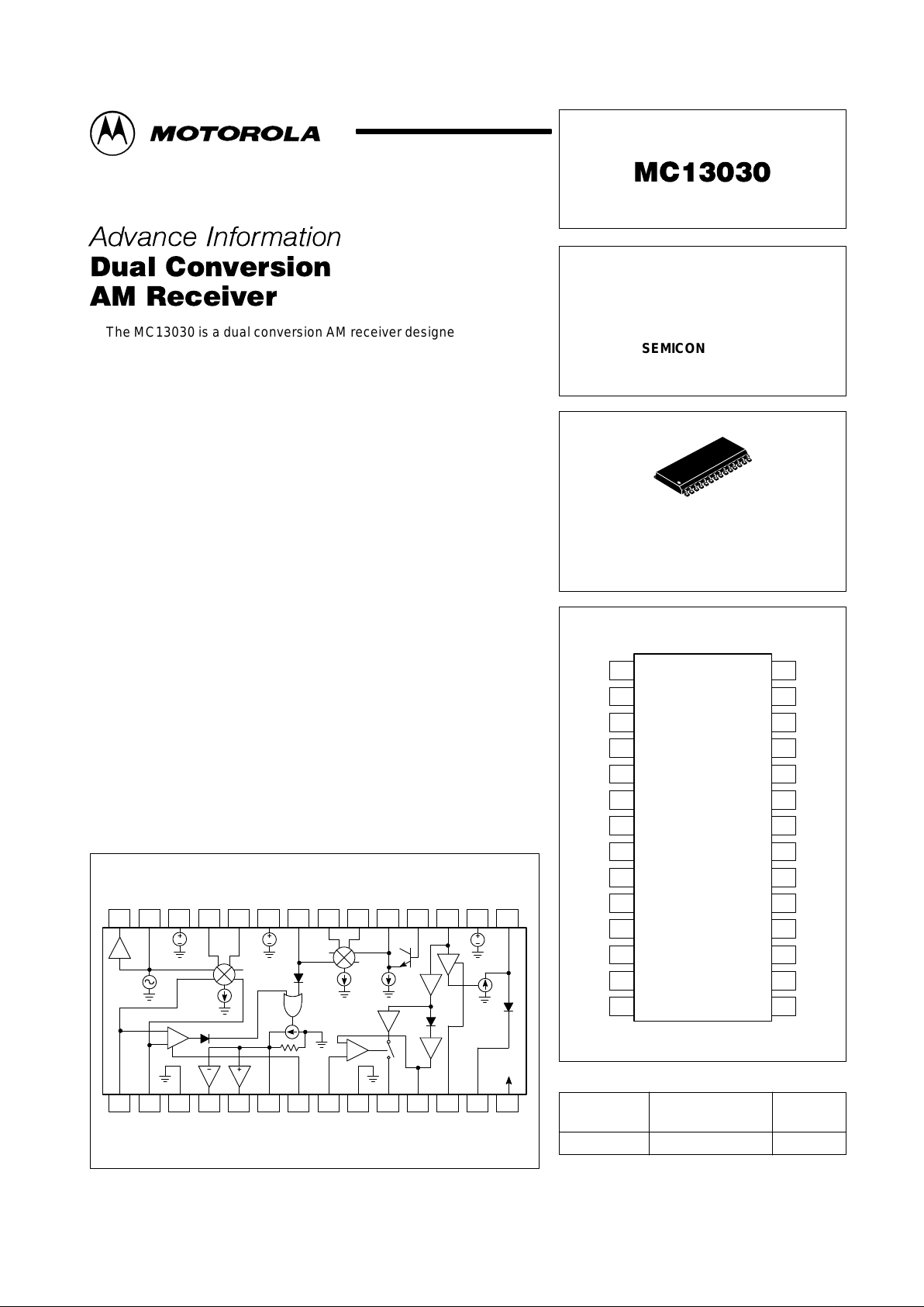
Representative Block Diagram
This device contains 335 active transistors.
1413121110987654321
1516171819202122232425262728
V
CC
VCO
5.1 V 6.5 V
Mix1
Mix2 XTal
Osc
4.1 V
3.0 mA
IF Amp
AGC
6.6 mA
Motorola, Inc. 1996 Rev 1
Page 2
MC13030
2
MOTOROLA ANALOG IC DEVICE DATA
MAXIMUM RATINGS (T
A
= 25°C, unless otherwise noted.)
Rating
Symbol Value Unit
Power Supply V
CC
10 V
Operating Temperature T
A
–40 to +85 °C
Storage Temperature T
stg
–65 to +150 °C
Junction Temperature T
J
150 °C
NOTE: ESD data available upon request.
ELECTRICAL CHARACTERISTICS (T
A
= 25°C, VCC = 8.0 V, unless otherwise noted.)
Characteristic
Condition/Pin Symbol Min Typ Max Unit
Power Supply Voltage – V
CC
7.5 8.0 9.0 V
Power Supply Current VCC = 8.0 V I
CC
26 32 44 mA
Detector Output Level Vin = 1.0 mV , 30% Mod. V13 160 200 240 mVrms
Audio S/N Ratio Vin = 1.0 mV , 30% Mod. S/N 48 52 – dB
Audio THD Vin = 1.0 mV , 30% Mod.
THD – 0.3
1.0
%
Vin = 1.0 mV , 80% Mod.
– 0.3
1.0
Vin = 2.0 mV , 80% Mod. – 0.4 1.5
Signal Strength Output Vin = 0 to 2.0 V V11 0 – 5.2 V
VCO Buffer Output – V28 178 224 282 mV
SD Output Level Vin = 1.0 mV , V11 > V8 V10 2.3 2.7 3.3 Vpp
MIXER1
Input Resistance 1 or 2 to Gnd – – 10 – kΩ
Third Order Intercept Point 1 or 2 IP3 – 127 – dBµV
Conversion Transconductance 1 or 2 to 24 + 25 g
c
– 2.2 – mS
Total Collector Current 24 + 25 I
C
– 4.6 – mA
Input IF Rejection 1 or 2 – – 45 – dB
MIXER2
Input Resistance 22 – – 2.4 – kΩ
Third Order Intercept Point 22 IP3 – 112 – dBµV
Conversion Transconductance 22 to 20 + 21 g
c
– 4.6 – mS
Total Collector Current 20 + 21 I
C
– 3.0 – mA
VCO
Minimum Oscillator Coil Parallel Impedance 27 to 26 R
P
– 3.0 – kΩ
Buffer Output Level 28 V
O
– 224 – mVrms
Stray Capacitance 27 C
S
– 7.0 – pF
IF AMPLIFIER
Input Resistance 17 R
in
– 2.0 – kΩ
Transconductance 17 to 15 g
m
– 28 – mS
Maximum Input Level 17 V
in
– 125 – mVrms
Minimum Detector Coil Parallel Impedance 17 to 15 R
L
– 15 – kΩ
RF Output Level 15, Vin = 1.0 mV – – 2.0 – Vpp
Audio Output Impedance 13 R
out
– 120 – Ω
Audio Output Level 13 @ 30% Mod. V
out
– 200 – mVrms
Page 3
MC13030
3
MOTOROLA ANALOG IC DEVICE DATA
NOTES: 1. The transformers used for at the output of the mixers are wideband 1:4 impedance ratio. The secondary load is the 50 Ω input of the spectrum
analyzer, so the impedance across the collectors of the mixer output is 200 Ω.
2.Since the VCO frequency is not critical for this measurement, a fixed tuned oscillator tuned to 11.7 MHz is used. This gives an input frequency
of 1.0 MHz.
3.The detector coil is loaded with a 10 k resistor to reduce the tuned circuit Q and to present a 10 kΩ load to the IF output for determination of IF
transconductance.
4.The RF AGC current, S output current and Pin 6 current are measured by connecting a current measuring meter to these pins, so they are effectively
shorted to ground.
5.SD adjust is adjusted by connecting a power supply or potentiometer and voltmeter to Pin 8.
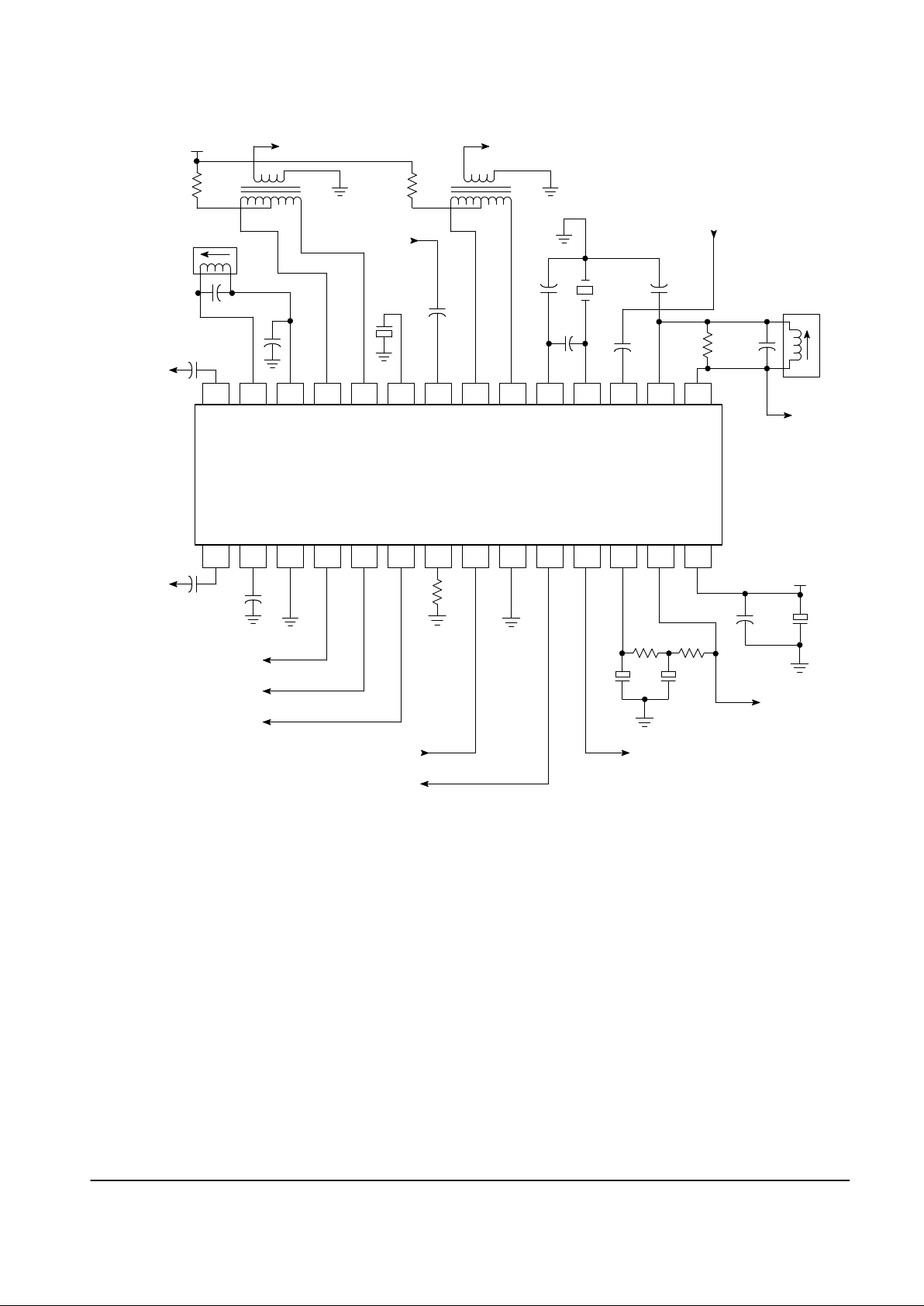
Figure 1. Test Circuit
1516171819202122232425262728
VCO
Out
VCO VCO
Ref
Mix1
Out
Mix1
OutRFV
ref
Mix2InMix2
Out
Mix2
Out
Xtal
Osc E
Xtal
Osc B
IF In Det
V
ref
Det
In
Mix1InMix1InRF
Gnd
FET
RF
AGC
RF
AGC2
RF
AGC
Adj
Mix1
RF AGC
Adj
SD
LevelIFGnd
SD IF
Out
S Level
OutIFAGC InAFOut
V
CC
Mixer1 Out Mixer2 Out
8.0 V
Mixer2 In
Osc Out
Mixer1 Input
FO = 1.0 MHz
FET RF AGC Voltage
RF AGC Current
Pin 6 Current
SD Adjust
IF Signal Out
S Output Current
Audio Out
IF Output/
Det Input
IF
Input
Adj to 11.7 MHz
2.2
µ
H
82 pF
680
µ
H
47
µ
F
8.0 V
10 k 10 k
++
22
0.1
0.1
10.245
47
0.1
1.0
µ
F
+
0.1
0.01
47
47
1:4 1:4
10 k 180 pF
0.1
0.1
R7
0.1
4.7
µ
F
+
1413121110987654321
FUNCTIONAL DESCRIPTION
The MC13030 contains all the necessary active circuits for
an AM car radio or shortwave receiver.
The first mixer is a multiplier with emitter resistors in the
lower, signal input transistors to give a high dynamic range. It
is internally connected to the first oscillator (VCO). The input
pins are 1 and 2. The input can be to either Pins 1 or 2, or
balanced. These pins are internally biased, so a dc path
between them is allowable but not necessary. The mixer
outputs are open collectors on Pins 25 and 26. They are
normally connected to a tuned transformer.
The first oscillator on Pin 27 is a negative resistance type
with automatic level control. The level is low so the signal
does not modulate the tuning diode capacitance and cause
distortion. Pin 26 is the reference voltage for the oscillator
coil. This reference is also the supply for the mixer circuits.
The upper bases of the mixer are 0.7 V below this reference.
The second mixer is similar to the first, but it is single–
ended input on Pin 22. Its outputs are open collectors on
Pins 20 and 21 which are connected to a tuned transformer.
The dynamic range of this mixer is less than the first. It is also
connected internally to an oscillator which is normally crystal
controlled. The oscillator is a standard Colpitts type with the
emitter on Pin 19 and the base on Pin 18.
The IF amplifier input is Pin 17. The AGC operates on the
input stage to obtain maximum dynamic range and minimum
distortion. The IF output, Pin 15, is a current source.
Page 4
MC13030
4
MOTOROLA ANALOG IC DEVICE DATA
Therefore, its gain is determined by the load impedance
connected between Pins 15 and 16. Pin 16 is a voltage
reference for the output. The output is internally connected to
the AM detector, and Pin 13 is the detector output. This
detector also provides the AGC signal for the IF amplifier. An
RC filter from Pin 13 to 12 removes the audio, leaving a dc
level proportional to the carrier level for AGC.
Pin 11 provides a current proportional to signal strength.
It is a current source so a resistor must be connected from
Pin 11 to ground to select the desired dc voltage range. The
current is proportional to the signal level at Pin 17, the IF
amplifier input.
A high–gain limiting amplifier is used to derive the station
detect (SD) signal output on Pin 10; this output is present only if
it is turned on by the voltage on Pin 8. If the voltage on
Pin 8 is less than the voltage on Pin 11, the output on Pin 10 is
“on”. The station detector IF output on Pin 10 is used with
synthesizers which have a frequency counting signal detector.
The RF AGC outputs on Pins 4 and 5 are controlled by the
signal levels at Mixer1 or Mixer2. Bypass capacitors are
required on Pins 6 and 4 to remove audio signals from the
AGC outputs. Pin 4 is designed to control the NPN transistor
in series with the RF amplifier FET. The voltage on Pin 4 is
5.1 V with no input signal and decreases with increasing input
signal. Pin 5 is designed to control an additional AGC circuit
at the antenna input. The voltage on Pin 5 is at 0 V with no
input signal and increases with increasing input signals. The
voltage on Pin 5 does not increase until the voltage on Pin 4
has decreased to about 1.3 V . In most cases, Pin 5 is used to
drive a diode shunt. Maximum output current is about 850 µA.
The RF AGC sensitivity is about 40 mVrms input to Mixer1
or about 2.0 mVrms input to Mixer2 at 1.0 MHz. The AGC
sensitivity for both mixers can be decreased by adding a
resistor from Pin 6 to ground. There is also an additional
amplifier between Mixer1 and its AGC rectifier. The gain of
this amplifier and AGC sensitivity for Mixer1 can be increased
by adding a resistor from Pin 7 to ground. Therefore, the
desired AGC sensitivity for both mixers can be achieved by
changing the resistors on Pins 6 and 7.
1
2
3
4
5
6
7
8
9
10
11
12
13
14
28
27
26
25
24
23
22
21
20
19
18
17
16
15
Mix1 In
Mix1 In
RF Gnd
FET RF AGC
RF AGC2
RF AGC Adj
Mix1 RF AGC Adj
SD Level
IF Gnd
SD IF Out
S Level Out
IF AGC In
AF Out
V
CC
VCO Out
VCO
VCO Ref
Mix1 Out
Mix1 Out
V
ref
Mix2 In
Mix2 Out
Mix2 Out
Xtal Osc E
Xtal Osc B
IF In
Det V
ref
Det In
Figure 2. Pin Connections and DC Voltages
5.1 V
5.1 V
5.1 V
7.8 V
7.8 V
6.5 V
3.7 V
7.9 V
7.9 V
4.4 V
5.0 V
4.8 V
4.1 V
4.1 V
3.3 V
3.3 V
0 V
5.1 to 0 V
0 to 850
µ
A
0 to 2.8 V
200 mV
43 mV
0 to 4.8 V
0 V
6.5 V
0 to 4.8 V
3.6 to 4.5 V
3.6 to 4.5 V
8.0 V
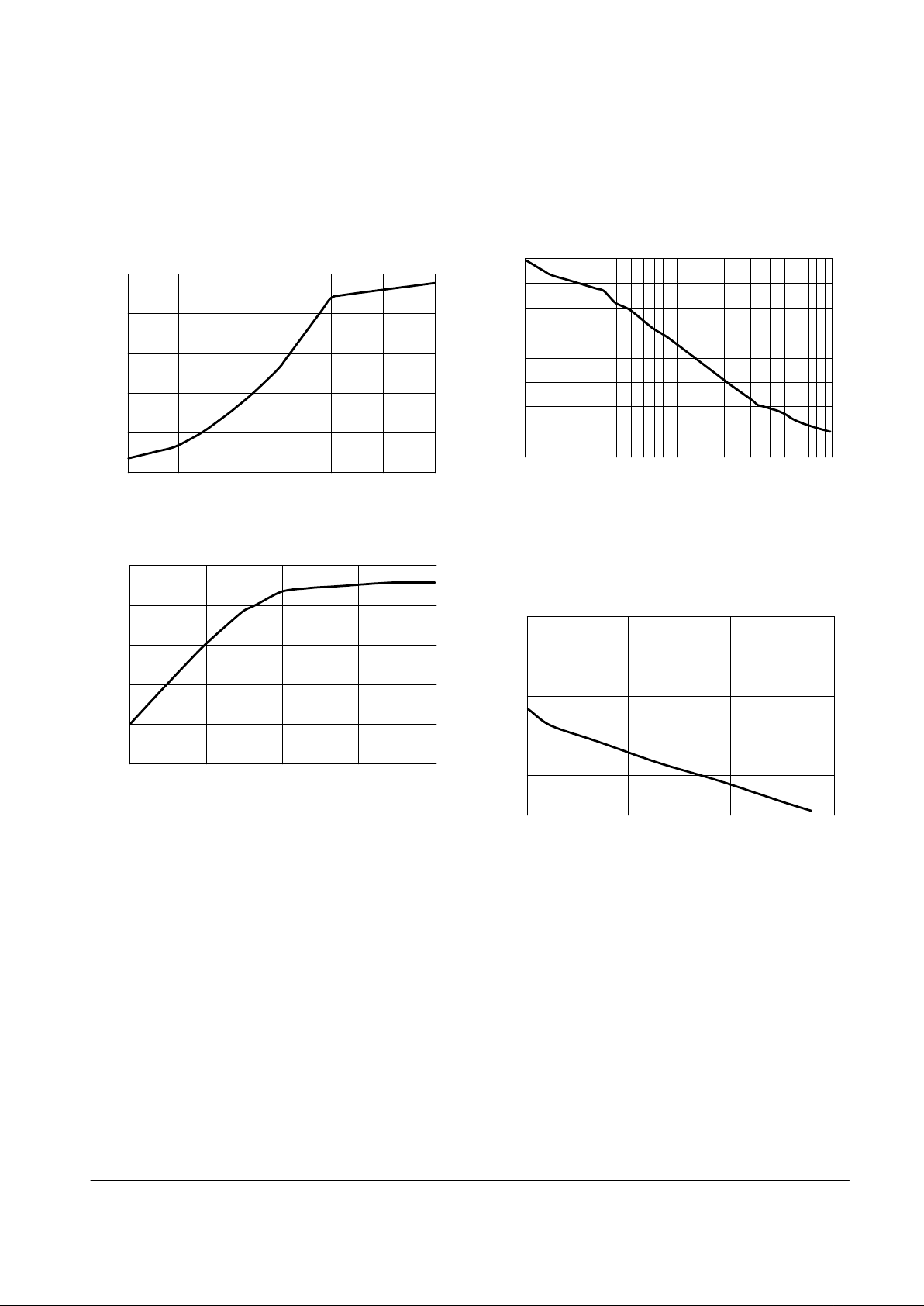
S Out versus IF Input:
The S output current at Pin 11 is provided by two
collectors, one a PNP source and the other a sink to ground.
The desired S output voltage can be selected using the curve
of Figure 3 and calculating the value of the required resistor.
Figure 3. S Output Current versus IF Input Level
IF INPUT LEVEL (dBµV)
30 40 50 100
0
20
40
60
70
PIN 11 CURRENT ( A)
60 70 80 90
µ
RF FET AGC versus Mixer1 and Mixer2 Input Level:
Figures 4 and 5 are generated with no external resistance
on Pins 4 or 6, so they represent the minimum RF AGC
sensitivity of Mixer1 and Mixer2.
Figure 4. RF AGC Voltage versus Mixer1 Input
85 90 95 100 105
0
1.0
2.0
3.0
4.0
5.0
MIXER1 INPUT LEVEL (dB
µ
V)
PIN 4 VOLTAGE (V)
Figure 5. RF AGC Voltage versus Mixer2 Input
MIXER2 INPUT LEVEL (dBµV)
65 70 75 80
0
1.0
2.0
3.0
4.0
5.0
PIN 4 VOLTAGE (V)
Page 5
MC13030
5
MOTOROLA ANALOG IC DEVICE DATA
Pin 6 Current versus Mixer1 and Mixer2 Input Level:
The internal resistance from Pin 6 to ground is 39 k.
The RF AGC voltage on Pin 4 is 2.0 V when the voltage on
Pin 6 is 1.2 V. Therefore, the desired AGC thresholds for
either mixer can be set with these curves. The design steps
are described in the design notes.
Figure 6. Pin 6 Current versus Mixer1 Input Level
MIXER1 INPUT LEVEL (dBµV)
90 100 110 120
0
50
100
150
200
250
PIN 6 CURRENT ( A)
µ
PIN 6 CURRENT ( A)
µ
Figure 7. Pin 6 Current versus Mixer2 Input Level
MIXER2 INPUT LEVEL (dBµV)
80 90 120
0
50
100
150
200
100 110
250
Mixer1 AGC Gain Increase versus R7:
Adding a resistor from Pin 7 to ground increases the AGC
sensitivity of Mixer1. The range of increase in dB can be
found from this curve. This is useful after setting up the AGC
threshold of Mixer2.
Figure 8. Mixer1 AGC Gain Increase versus R7
R7
100 10 k
0
5.0
6.0
7.0
8.0
INCREASE IN MIXER1 AGC SENSITIVITY (dB)
1.0 k
1.0
2.0
3.0
4.0
Pin 5 Current versus Pin 4 Voltage:
All the curves give Pin 4 AGC voltage versus some other
input level. This curve can be used to determine the auxiliary
AGC current from Pin 5 at a given Pin 4 voltage.
Figure 9. Pin 5 Current versus Pin 4 Voltage
PIN 5 CURRENT (mA)
0 0.4 0.8 1.2
0
1.0
2.0
3.0
4.0
5.0
PIN 4 VOLTAGE
Page 6

MC13030
6
MOTOROLA ANALOG IC DEVICE DATA
PIN FUNCTION DESCRIPTION
Pin No. Internal Equivalent Circuit Description
1, 2
12
10 k10 k
3.3 V
6.6 mA
150 150
Mixer1 Input
Pins 1 and 2 are equivalent. In the application circuit, 2 is grounded
with a capacitor and 1 is the input. If a load resistor is needed for the
input filter, it can be placed across Pins 1 and 2. Input impedance for
each pin is 10 k. IP3 (third order intercept) at the input is 20 dBm
(127 dBµ). To guarantee –50 dB IM3, the input level should not be
greater than 3.5 dBm (103 dBµ) (150 mVrms).
3
3
RF Ground
This should be connected to the ground used for the RF circuits.
4
4
5
10 k
5.1 V 4.0 V
3.4 k
FET RF AGC Output
This is the AGC for the cascode transistor connected to the RF amplifier
FET. The no–signal voltage is 5.1 V. The voltage decreases with
increasing input signals. A bypass capacitor and electrolytic capacitor
must be added to filter out RF signals on the transistor and audio signals
in the AGC signal. See Figures 4 and 5.
5
5
100 22 k
V
CC
330
RF AGC2 Output
The voltage on this pin starts at 0 and increases with increasing input
signals. It is normally used to turn on diodes or a transistor connected
across the antenna input and is AGC delayed until Pin 6 reaches 2.7 V .
If the voltage on Pin 5 decreases below 2.0 V , the voltage on this pin will
decrease from 3.1 down to about 1.5 V . The maximum output current is
about 850 µA.
6
6
330
AGC
1.0 k
39 k 3.3 k
RF AGC Adjust
An electrolytic capacitor of 1.0 µF must be connected to prevent audio
modulation of the AGC circuits. If there is no resistor on this pin, the RF
AGC starts at an input level to Mixer1 ≈ 40 mVrms or Mixer2 ≈ 2.0 mVrms.
Connecting a resistor from Pin 6 to ground increases RF levels required
for AGC to start. It should be used to set the desired AGC level of Mixer2.
If a resistor is not connected to Pin 6, unwanted RF signals will cause the
AGC to start at a very low level, and desired signals may be suppressed.
7
7
500
1.5 k
Mixer1 RF Level Adjust
A resistor from Pin 7 to ground will increase the gain of an amplifier from
the input of Mixer1 to the AGC circuit. It can be used to set the RF AGC
level of Mixer1. The minimum value of R7 is about 680 Ω.
8
8
510
3.3 k
SD
S
Station Detector Signal Level Adjust
A voltage on Pin 8 will set the desired signal strength at which the SD IF
Out on Pin 10 appears. The other input to this comparator is the S (signal
strength) signal. If Pin 8 is grounded, a square wave of the 2nd IF (usually
450 of 455 kHz) is present with very small input levels. This output could
also be used to drive an FM detector if desired.
9
9
IF Ground
Pin 9 is the ground for the IF section.
Page 7

MC13030
7
MOTOROLA ANALOG IC DEVICE DATA
PIN FUNCTION DESCRIPTION (continued)
Pin No. DescriptionInternal Equivalent Circuit
10
IF
10
10 k
SD
510
Station Detector IF Output
This output is “on” when V11 > V8. The output is an amplified and limited
2nd IF signal. The signal level is ≈ 250 mVpp when it is 100% “on”.
11
11
510
1.0 k
1.0 k
V
CC
S Level Output
This is a dc current proportional to IF input level. With a load resistor of
75 k, the dc voltage is 0 to 5.1 V.
12
12
1.0 k
V
CC
IF AGC In
The IF gain is controlled by the dc voltage on this pin. It is normally
connected to Pin 13 through an RC network to filter out the audio signal
on Pin 13. The IF gain is maximum when V13 ≈ 3.6 V. When V13
increases, the IF gain decreases.
13
100
13
V
CC
Audio Output
The dc voltage on Pin 13 is ≈ 3.6 V with no input signal and increases to
≈ 4.5 V at minimum IF gain. A nonpolarized electrolytic capacitor may be
required to couple to the audio circuits if the audio amplifier dc bias
voltage is between these voltages.
14
V
CC
14
Supply Voltage
The nominal operating voltage is 8.0 V .
15
510
510
510
15
IF Amplifier Output and Detector Input
The detector coil must be connected between Pin 15 and 16. The IF
amplifier output is a current source, the IF amplifier is a transconductance
amplifier; the gain is determined by the impedance between Pins 15 and
16. The IF amplifier gm ≈ 0.028 mho. If a wide bandwidth IF is desired, the
detector coil can be connected between Pins 15 and 16 without a tap and
then loaded with a resistor across the coil.
16
16
1.0 k
510
Detector Reference Voltage
One side of the detector coil is connected to this pin. It should be
bypassed with a 0.1 µF capacitor.
Page 8

MC13030
8
MOTOROLA ANALOG IC DEVICE DATA
PIN FUNCTION DESCRIPTION (continued)
Pin No. DescriptionInternal Equivalent Circuit
17
2.0 k
4.8 V
17
To SD
Circuit
IF Input
The IF input impedance is 2.0 k to match most ceramic 455 or 450 kHz
filters. For a ceramic filter requiring a 1.5 k load, a 5.6 k resistor in
series with a 0.01 µF capacitor should be connected from Pin 17 to
ground.
18
19
18
5.1 k
500
Crystal Oscillator Base
The crystal oscillator is a simple Colpitts type, operating at a low
current. The crystal should operate at 10.250 MHz for 450 kHz IF or
10.245 MHz for 455 kHz IF with a 20 pF load capacitance. The
oscillator signal to the second mixer is coupled from Pin 18 through an
emitter follower. If a synthesizer such as the Motorola MC145170 with
a 15 bit programmable R counter is used, the 10.245 MHz crystal can
be connected to the synthesizer, and a 200 mVpp oscillator signal
from the synthesizer can be capacitively coupled to Pin 18, so only
one crystal is needed.
19 Crystal Oscillator Emitter
The capacitive divider from Pin 18 is connected as shown in the
application circuits of Figures 10, 11, 12.
20, 21
20 21
Mixer2 Output
The maximum AC collector voltage is about 5.8 Vpp or 2.0 Vrms. The
mixer conversion transconductance gc = 0.0046 mho. The load
impedance should be selected so the mixer output does not overload
before the input.
22
5.1 V
To AGC
Circuit
2.4 k
22
51 51
3.0 mA3.7 V
Mixer2 Input
The input impedance is 2.4 k. A series R–C network from Pin 22 to
ground or a resistor from the filter to Pin 22 can be used to properly
match the filter. In most cases, a 10.7 MHz crystal filter can be connected
to Pin 22 directly without any additional components. IP3 (third order
intercept) at the input is 5.0 dBm (1 12 dBµ). T o guarantee –50 dB IM3, the
input level should not be greater than –20 dBm (87 dBµ) (22.7 mVrms).
23
23
6.5 V
V
ref
V
ref
This is the main reference voltage for most of the circuits in the IC and
should be bypassed with a 1.0 µF capacitor.
24, 25
VCO
24
5.1 V
25
Mixer1 Output
The maximum collector voltage is about 5.8 Vpp or 2.0 Vrms. The mixer
conversion transconductance gc = 0.0022. The load impedance should
be selected so the mixer output does not overload before the input.
Page 9

MC13030
9
MOTOROLA ANALOG IC DEVICE DATA
PIN FUNCTION DESCRIPTION (continued)
Pin No. DescriptionInternal Equivalent Circuit
26
V
CC
V
ref
26
75
VCO Reference
The first oscillator coil is connected from Pin 26 to 27. Pin 26 must be
bypassed to ground with a capacitor which has a low impedance at the
oscillator frequency. This capacitor also will reduce the phase noise of
the VCO.
27
7.5 k
27
to Mixer1
VCO
The VCO is a negative resistance type and has an internal level control
circuit so a tapped coil or one with a secondary is not needed. The level
is fixed at 0.8 Vpp so the oscillator signal does not modulate the tuning
diode, thus keeping the distortion low. The oscillator stray capacitance is
≈ 12 pF and the tuned circuit impedance should be greater than 3.0 k to
guarantee oscillation. Oscillator range is up to 45 MHz so it can be used
for SW receivers.
28
100
28
VCO Out
The output level is 240 mVrms (108 dBµ), high enough to drive any
CMOS synthesizer.
AM CAR RADIO DESIGN NOTES
The MC13030 AM Radio IC is intended for dual
conversion AM radios. In most cases, the 1st IF frequency
(F
IF1
) is upconverted above the highest input frequency. The
first oscillator (VCO) is tuned by a synthesizer and operates
at Fin + F
IF1
. For the 530 to 1700 kHz AM band with a
10.7 MHz first IF, the VCO goes from 11.23 to 12.40 MHz.
Therefore, F
max/Fmin
for VCO is only 1.104, so one low–cost
tuning diode can be used. Since the required tuning voltage
range can be made less than 5.0 V , it may also be possible to
drive the tuning diode directly or from the phase detector of
the synthesizer IC, such as the Motorola MC145170,
operating from 5.0 V, without using a buffer amplifier or
transistor.
If the VCO is above the incoming frequency, the image
frequency of the first mixer is at f
OSC
+ F
IF1
. For th e A M
broadcast receiver, it is around 22 MHz, so a simple LPF
can be used between the RF stage and Mixer1 input.
However, if a LPF is used, an additional coil is still needed
to supply the collector voltage of the RF amplifier. For this
reason, a BPF filter was used in the application circuit
instead, since it uses the same number of coils and gives
better performance. It is simply a lowpass to bandpass
conversion. The lowpass filter is designed to have a cutoff
frequency equal to the desired bandwidth. In this case, it
would be 1700 – 530 kHz = 1170 kHz. Then, it is
transformed to be resonant at 949 kHz, the geometric
mean of the end frequencies:
1700 x 530 = 949 kHz.
p
A balanced–to–unbalanced transformer is required at the
output of both mixers. The first one is designed so that Mixer1
has enough gain to overcome the loss of the 10.7 MHz filter
and so that the output of the mixer will not overload before the
input. The primary impedance of the transformer is relatively
low, and it may be difficult to control with commonly available
7.0 mm transformers because the number of primary turns is
quite small. It would also require a large tuning capacitance.
A better solution is to tune the secondary with a small
capacitance and then use a capacitive divider to match the
tuned circuit to the filter. This allows one transformer to be
used for either a ceramic or crystal filter. The capacitors can
be adjusted to match the filter. The recommended coil is
made this way.
If the formula: Pin = IP3 – DR/2 is used, the maximum input
level to the mixer can be calculated for a desired dynamic
range.
IP3 = 3rd order intercept level in dB (dBm or dBµ)
DR = dynamic range in dB between the desired signals
and 3rd order intermodulation products
Pin = input level in dBm or dBµ
The RF AGC level can then be adjusted so that Pin does
not exceed this level.
Whether or not a narrow bandwidth crystal or wide
bandwidth ceramic filter is used between the first and second
mixers depends on the receiver requirements. It is possible to
achieve about 50 dB adjacent channel and IM rejection with
a ceramic filter because of the wide dynamic range of the
mixers. If more than this is required, a crystal filter should be
used. If a crystal filter is used, a lower cost CFU type of
455 kHz second IF filter can be used. If a ceramic filter is
used, a CFW type filter should be used because there is no
RF section selectivity in this type of radio.
Since the wideband AGC system is quite sensitive, it can
be set to eliminate all spurious responses present at the
receiver output. However, the RF AGC will sometimes
eliminate or reduce the level of desired signals if there is a
strong signal somewhere in the bandpass of the RF circuit.
The second mixer is designed like the first and requires a
balanced output. Since its load impedance is higher, the
transformer can be designed to be tuned on the primary or
Page 10

MC13030
10
MOTOROLA ANALOG IC DEVICE DATA
secondary, but, like with the one for the first mixer, if the
secondary is tuned, the tap can be adjusted for the
impedance of the 455 kHz filter. Wideband filters usually have
a higher terminating resistance than the narrowband ones.
The recommended coil is made this way.
The IF amplifier is basically a transconductance amplifier
because the output is a current source. The output is also
internally connected to a high impedance AM detector. gm for
the IF amplifier is ≈ 0.028 mho. The voltage gain will be the
detector coil impedance x 0.028. This can be designed to
give the desired audio output level for a given RF input level.
If it is set too high, the receiver may oscillate with no input
signal. The application circuit was designed for a relatively
narrow bandwidth, so a tapped detector coil is used to get the
desired gain. If a wide bandwidth receiver is desired, the
detector coil can be untapped, and a resistor can be added
across the coil to get the desired Q.
The detector output on Pin 13 is a low impedance. It
supplies the IF AGC signal to Pin 12, so the audio must be
filtered out. The time constant of this filter is up to the
designer. The main requirement is usually the allowable
audio distortion at 100 Hz, 80% modulation. If the time
constant is made too long, the audio level will be slow to
correct when changing stations.
The Signal Strength (S) output is dependent only on the
IF amplifier input level. Its maximum voltage is about 5.0 V
with a 75 k load resistor. The range can be reduced by
using a lower value for the resistor on Pin 11. The S signal
will stop increasing when the RF AGC circuits become
active, so if the RF AGC threshold is set too low, or there is
too much loss from the Mixer2 output to the IF input, the
maximum S signal will be reduced. The desired load
resistor on Pin 11 (R 11) can be determined using the curve
of Pin 11 current versus IF input.
Setting the RF AGC threshold is probably the most difficult
because a trade–off between allowable interference and
suppression of desired signals must be made.
First select the values for both mixers:
a. Using the formula Pin = IP3 – DR/2
Select the desired dynamic range and calculate the
maximum input levels for both mixers. Remember that all
levels must be in dB, dBµV or dBm. Let DR = 50 dB. IP3
for M ixer2 = 112 dBµV. Therefore, P
inmax
= 87 dBµV. IP3
for M ixer1 = 127 dBµV. Therefore, P
inmax
= 102 d BµV.
b. First, adjust the resistor from Pin 6 to ground to give
the desired maximum input level to Mixer2. From the
curve of Pin 6 current versus Mixer2 input level,
R6 = 1.2/110 µA = 11 k. R
int
= 39 k, so R
6ext
= 15 k.
c. From the curve of Pin 6 current versus Mixer1 input level,
determine how much more gain would be required in the
Mixer1 AGC circuit to achieve the desired dynamic range
for Mixer1. From the curve of Relative Sensitivity versus
R7 determine the value of R7. Alternatively, R7 can be
adjusted to give the desired maximum input level to
Mixer1.
The resulting R7 may be too small to set the AGC
threshold of Mixer1 as low as desired. Also, if R7 is less than
680 Ω, the AGC sensitivity for the Mixer1 input falls off at
higher frequencies, so in these cases, the resistor from Pin 6
to ground must be reduced to achieve the desired level
because the overload of Mixer1 provides the most important
spurious response rejection. However, if the AGC level is set
too high, the IF in signal may become too large and the IF
amplifier can overload with strong signals. The values used in
the application are more conservative.
The gain from the antenna input to the point being
measured are shown on the AM radio application. These are
helpful when calculating audio sensitivity and troubleshooting
a new radio.
Page 11

MC13030
11
MOTOROLA ANALOG IC DEVICE DATA
FL1
T3
Figure 10.
2
8.0 V
A1
L6
C30
T1
0.01
CFU455H2
Crystal Filter
Ceramic Filter
8.0 V
8.0 V
10.5 X
Tuning Voltage
D1
C26
10.245
+
R17
C12
R5
R12
56 pF
34
In
5
1
88 X
28 27 26 25 24 23 22 21 20 19 18 17 16 15
123456 7891011121314
AF Out
0 to 4.8 V
IF Output to
RF In
47
1.0–7.0 V
MV209
C4
C20
0.1
C8
1.0
F
µ
9.8 H
µ
19335
T2
12704
C29
330 pF
47
C27
2200 pF
270 pF
C14
47 pF
X1
CFW455H
Out
Gnd Gnd Gnd
130 X
C13
22 pF
10M7A
180 k
0.1
SK107M5–AE–10A
SFE10.7MHY
123
123
C19
22 pF
C25
0.01
R13
33 k
C2
0.1
R3
1.0 k
C16
120 pF
L2
220 H
µ
L4
220 H
µ
C17
120 pF
4.5 X
R4
1.0 k
L3
220 H
µ
C18
120 pF
C15
0.1
R8
47
+
C7
1.0
F
µ
R6
33 k
R7
1.0 k
R14
56 k
R
V1
100 k
R10
68 k
C23
0.01
Signal Detector
C22
0.1
D2
1N4148
C21
0.01
+
C5
µ
C3
0.01
C1
0.1
L1
1.5 mH
R1
1.0 k
L5
33 H
µ
R2
180
Signal Strength
+
C9
+
C10
R9
10 k
R11
10 k
R15
2.7 k
+
C6
C11
0.1
B1
Bead
C28
0.01
R16
390
R18
1.5 k
IC1
MC13030
V
CC
47 F
6.5 X
µ
4.7 F
µ
47 F
AF
IF AGCI
S Out
IF Out
IF Gnd
SD Adj
M1 AGCL
RF AGCL
RF AGC2
FET AGC
RF Gnd
M1 In
M1 In
Osc Out
Osc
Osc VR
M1 Out
M1 Out
RF VR
M2 In
M2 Out
M2 Out
Xtal E
Xtal B
IF In
IF VR
Det In
D3
1N4148
Q1
J309
Q2
2N4401
Figure 10. AM Radio Application
12705
C24
27 nF
C31
0.01
FL2
µ
4.7 F
Page 12

MC13030
12
MOTOROLA ANALOG IC DEVICE DATA
SW RADIO DESIGN NOTES
The shortwave receiver was designed to cover from 5.0 to
10 MHz. This MC13030 radio has better performance than
most receivers because of the high dynamic range and
spurious rejection of the mixers.
The RF stage bandpass filter for this radio is the same type
as the one used for the car radio, but the series tuned section
was scaled down in impedance to reduce the inductance of
the coil.
Since most SW receivers include an SSB and CW mode,
the detector coil could have a secondary winding to supply
the second IF signal to this section.
The capacitors C10 and C23 have been reduced from
those in the AM radio so that the AGC system can follow
variations in signal level due to fading.
CB RADIO DESIGN NOTES
The RF stage bandpass filter for this radio consists of a
tuned input and a double tuned interstage filter. For lower cost
radios, a single tuned interstage filter could be used.
The schematic also shows a crystal 10.7 MHz 1st IF filter, but
a ceramic or coil filter could als o be used. An intermodulation
rejection of 50 dB can be obtained with a ceramic 1st IF filter.
A bipolar transistor is shown for the RF stage. A dual gate
CMOS FET could also be used with G2 connected to the
AGC voltage on Pin 4. A PIN diode is recommended for D2.
COIL DATA
T1 – Toko A119ANS–19335UH
T2 – Toko A7MNS–12704UH
T3 – Toko A7MCS–12705Y
Page 13

MC13030
13
MOTOROLA ANALOG IC DEVICE DATA
Figure 11.
2
8.0 V
A1
L6
C26
T1
0.01
Crystal Filter
8.0 V
Tuning
D1
C27
10.245
+
C12
R5
R13
56 pF
34
In
5
1
28 27 26 25 24 23 22 21 20 19 18 17 16 15
1 2 3 4 5 6 7 8 9 10 11 12 13 14
AM AF Out
0 to 4.8 V
IF Output to
RF In
47
MV209
C4
C20
0.1
C8
1.0
F
µ
2.7 H
µ
19335
T2
12704
C25
330 pF
47
C28
2200 pF
330 pF
C14
47 pF
X1
CFW455HT
Out
Gnd Gnd Gnd
FL2
C13
22 pF
10M7A
0.1
123
C19
100 pF
R14
33 k
C2
0.1
R3
1.0 k
C32
68 pF
L2
15 H
µ
L4
15 H
µ
C17
39 pF
R4
1.0 k
L3
15 H
µ
C18
39 pF
C15
0.1
R8
47
+
C7
1.0
F
µ
R6
33 k
R7
1.0 k
R10
75 k
C9
0.01
FM Detector
C22
0.1
D2
1N4148
C21
0.01
+
C5
µ
C3
0.01
C1
0.1
L1
1.5 mH
R1
1.0 k
L5
33 H
µ
R2
180
Signal Strength
+
C23
+
R9
10 k
R11
10 k
R12
2.7 k
+
C6C11
0.1
B1
Bead
R15
1.5 k
IC1
MC13030
V
CC
47 F
µ
1.0 F
µ
47 F
AF
IF AGCI
S Out
IF Out
IF Gnd
SD Adj
M1 AGCL
RF AGCL
RF AGC2
FET AGC
RF Gnd
M1 In
M1 In
Osc Out
Osc
Osc VR
M1 Out
M1 Out
RF VR
M2 In
M2 Out
M2 Out
Xtal E
Xtal B
IF In
IF VR
Det In
D3
1N4148
Q1
J309
Q2
2N4401
Figure 11. 5 to 10 MHz Radio Application
Voltage
C31
100 pF
IF Output to SSB
Demodulator
C30
0.01
T3
12705
C16
68 pF
C10
µ
1.0 F
C24
27 nF
C29
0.01
Osc Output
to Synthesizer
Page 14

MC13030
14
MOTOROLA ANALOG IC DEVICE DATA
Figure 12.
8.0 V
A1
L5
C26
T1
0.01
CFU455H2
8.0 V
8.0 V
Tuning
D1
C27
+
R5
R12
56 pF
2
In
31
28 27 26 25 24 23 22 21 20 19 18 17 16 15
123456 7891011121314
AF Out
0 to 4.8 V
IF Output to
RF In
47
MV209
C4
C20
0.1
C8
1.0
F
µ
1.0 H
µ
19335
T2
12704
C25
330 pF
47
C28
2200 pF
270 pF
C14
47 pF
Out
Gnd
C13
22 pF
C19
47 pF
R13
33 k
C2
0.1
C15
0.01
R7
47
+
C7
1.0
F
µ
R5
68 k
R6
1.0 k
R14
56 k
R
V1
100 k
R9
75 k
C23
0.01
Signal Detector
C21
0.01
D2
BA243
L1
1.0 mH
Signal Strength
+
C9
+
C10
R8
10 k
R10
10 k
R15
2.7 k
+
C6
C11
0.1
IC1
MC13030
V
CC
µ
4.7 F
µ
47 F
AF
IF AGCI
S Out
IF Out
IF Gnd
SD Adj
M1 AGCL
RF AGCL
RF AGC2
FET AGC
RF Gnd
M1 In
M1 In
Osc Out
Osc
Osc VR
M1 Out
M1 Out
RF VR
M2 In
M2 Out
M2 Out
Xtal E
Xtal B
IF In
IF VR
Det In
Figure 12. CB Radio Application
C30
33 pF
Crystal Filter
10M7A
123
R16
1.5 k
C12 0.1
T3
12705
C16
47 pF
+
C5
µ
47 F
L3
330 nH
L2
330 nH
Q1
MPS9426
R3
10 k
C1
0.01
R2
3.9 k
C17
0.01
L4
1.0 H
µ
R1
100
C3
100 pF
C29
1.8 pF
C18
120 pF
C22
470 pF
Voltage
Osc Out to Synthesizer
16.265 to 16.705 MHz
C
24
27 nF
C31
0.01
µ
4.7 F
FL1
FL2
10.245
X1
Page 15

MC13030
15
MOTOROLA ANALOG IC DEVICE DATA
R5
R13
C25
C19
R8
C30
C29
FL1
R16
R12
L6
T1
C28
C8
T2
C13
R17
C9
C12
C10
C24
C6
RV1
C7
C23
C5
R2
L1
L5
R1
C3
R3
C16
L2
L3
C17
C15
C20
C2
C4
R18
C26C27
C14
X1
R9
R11
R15
R10
R14
C31
C22
R6
R7
C21
C1
R4
L4
C18
C11
T3
FL2
D1
D2
D3
J
J
AF
GND
+8.0 V
IF OUT
S
ANT IN
GND
GND VCO V+
Q2
Q1
Figure 13. Printed Circuit Board
(Top View)
4.0
″
(Bottom View)
4.0
″
3.0
″
3.0
″
NOTE: J = Jumper
Page 16

MC13030
16
MOTOROLA ANALOG IC DEVICE DATA
DW SUFFIX
PLASTIC PACKAGE
CASE 751F–04
ISSUE E
OUTLINE DIMENSIONS
NOTES:
1. DIMENSIONING AND TOLERANCING PER
ANSI Y14.5M, 1982.
2. CONTROLLING DIMENSION: MILLIMETER.
3. DIMENSION A AND B DO NOT INCLUDE
MOLD PROTRUSION.
4. MAXIMUM MOLD PROTRUSION 0.15 (0.006)
PER SIDE.
5. DIMENSION D DOES NOT INCLUDE
DAMBAR PROTRUSION.
ALLOWABLE
DAMBAR PROTRUSION SHALL BE 0.13
(0.005) TOTAL IN EXCESS OF D DIMENSION
AT MAXIMUM MATERIAL CONDITION.
J
K
F
1
15
14
28
–A–
–B–
28X
14X
D
P
S
A
M
0.010 (0.25) B
S
T
M
0.010 (0.25) B
M
26X G
–T–
SEATING
PLANE
C
X 45R
_
M
DIM MIN MAX MIN MAX
INCHESMILLIMETERS
A 17.80 18.05 0.701 0.711
B 7.40 7.60 0.292 0.299
C 2.35 2.65 0.093 0.104
D 0.35 0.49 0.014 0.019
F 0.41 0.90 0.016 0.035
G 1.27 BSC 0.050 BSC
J 0.23 0.32 0.009 0.013
K 0.13 0.29 0.005 0.011
M 0 8 0 8
P 10.01 10.55 0.395 0.415
R 0.25 0.75 0.010 0.029
____
Motorola reserves the right to make changes without further notice to any products herein. Motorola makes no warranty , representation or guarantee regarding
the suitability of its products for any particular purpose, nor does Motorola assume any liability arising out of the application or use of any product or circuit, and
specifically disclaims any and all liability, including without limitation consequential or incidental damages. “T ypical” parameters which may be provided in Motorola
data sheets and/or specifications can and do vary in different applications and actual performance may vary over time. All operating parameters, including “Typicals”
must be validated for each customer application by customer’s technical experts. Motorola does not convey any license under its patent rights nor the rights of
others. Motorola products are not designed, intended, or authorized for use as components in systems intended for surgical implant into the body, or other
applications intended to support or sustain life, or for any other application in which the failure of the Motorola product could create a situation where personal injury
or death may occur. Should Buyer purchase or use Motorola products for any such unintended or unauthorized application, Buyer shall indemnify and hold Motorola
and its officers, employees, subsidiaries, affiliates, and distributors harmless against all claims, costs, damages, and expenses, and reasonable attorney fees
arising out of, directly or indirectly, any claim of personal injury or death associated with such unintended or unauthorized use, even if such claim alleges that Motorola
was negligent regarding the design or manufacture of the part. Motorola and are registered trademarks of Motorola, Inc. Motorola, Inc. is an Equal
Opportunity/Affirmative Action Employer.
How to reach us:
USA/EUROPE/Locations Not Listed: Motorola Literature Distribution; JAPAN: Nippon Motorola Ltd.; T atsumi–SPD–JLDC, 6F Seibu–Butsuryu–Center,
P.O. Box 20912; Phoenix, Arizona 85036. 1–800–441–2447 or 602–303–5454 3–14–2 Tatsumi Koto–Ku, Tokyo 135, Japan. 03–81–3521–8315
MFAX: RMF AX0@email.sps.mot.com – TOUCHT ONE 602–244–6609 ASIA/PACIFIC: Motorola Semiconductors H.K. Ltd.; 8B Tai Ping Industrial Park,
INTERNET: http://Design–NET.com 5 1 Ting Kok Road, Tai Po, N.T., Hong Kong. 852–26629298
MC13030/D
*MC13030/D*
◊
 Loading...