

Page 1
Order this document by MC13028A/D
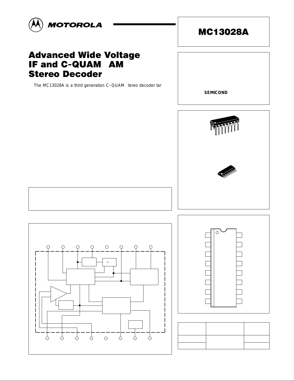
The MC13028A is a third generation C–QUAM stereo decoder targeted
for use in low voltage, low cost AM/FM E.T.R. radio applications. Advanced
features include a signal quality detector that analyzes signal strength,
signal to noise ratio, and stereo pilot tone before switching to the stereo
mode. A “blend function” much like FM stereo has been added to improve
the transition from mono to stereo. The audio output level is adjustable to
allow easy interface with a variety of AM/FM tuner chips. The external
components have been minimized to keep the total system cost low.
• Adjustable Audio Output Level
• Stereo Blend Function
• Stereo Threshold Adjustment
• Operation from 2.2 V to 12 V Supply
• Precision Pilot Tone Detector
• Forced Mono Function
• Single Pinout VCO
• IF Amplifier with IF AGC Circuit
• VCO Shutdown Mode at Weak Signal Condition
The purchase of the Motorola C–QUAMAM Stereo Decoder does not carry with such purchase any license by implication, estoppel or otherwise, under any patent rights of Motorola
or others covering any combination of this decoder with other elements including use in a
radio receiver. Upon application by an interested party, licenses are available from Motorola
on its patents applicable to AM Stereo radio receivers.
C–QUAM AM STEREO
ADVANCED WIDE VOLTAGE
IF and DECODER
for E.T.R. RADIOS
SEMICONDUCTOR
TECHNICAL DATA
16
1
P SUFFIX
PLASTIC PACKAGE
CASE 648
16
1
D SUFFIX
PLASTIC PACKAGE
CASE 751B
(SO–16)
Representative Block Diagram
VCO
AM Stereo
Decoder
IF
Amp
AGC
This device contains 679 active transistors.
B 8
Signal Quality
MOTOROLA ANALOG IC DEVICE DATA
Detector
Pilot Tone
Detector
Reg
PIN CONNECTIONS
Stereo
Filter
Bypass
Gnd
Stereo
1.0 V
Blend
1
2
3
4
5
6
7
8
Threshold Adjust
910111213141516
AGC Bypass
IF Feedback
IF Signal Input
Indicator Drive
Reference
Right Channel
16
Output
Left Channel
15
Output
Loop Filter
14
13
VCO Output
V
12
CC
Pilot Signal
11
Input
Pilot Q Detector
10
Output
Pilot I Detector
9
Output
ORDERING INFORMATION
Operating
Device
87654321
MC13028AD
MC13028AP DIP–16
Motorola, Inc. 1996 Rev 2
Temperature Range
TA = –25° to +70°C
Package
SO–16
1
Page 2
MC13028A
CC
TA
µ
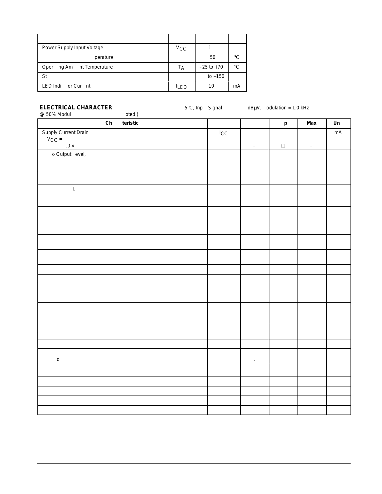
MAXIMUM RATINGS (
Power Supply Input Voltage
Operating Junction Temperature
Operating Ambient Temperature
Storage Temperature Range
LED Indicator Current
ELECTRICAL CHARACTERISTICS (V
@ 50% Modulation, unless otherwise noted.)
Supply Current Drain
VCC = 2.2 V
VCC = 8.0 V – 11 –
Audio Output Level, L+R, Mono Modulation V
RO = 1.8 k, VCC = 2.2 V, Input 55 dBµV 22 33 44
RO = 10 k, VCC = 8.0 V, Input 50 dBµV 150 200 250
RO = 10 k, VCC = 8.0 V, Input 40 dBµV 80 130 180
RO = 10 k, VCC = 8.0 V, Input 31 dBµV – 50 –
Audio Output Level, L or R Only, Stereo Modulation V
RO = 1.8 k, VCC = 2.2 V, 55 dBµV Input 35 80 106
RO = 10 k, VCC = 8.0 V 340 460 580
Output THD %
50% Stereo, L or R Only THD1 – 0.6 1.8
50% Mono, L+R THD2 – 0.3 0.6
90% Mono, L+R, Input 86 dBµV THD3 – – 1.5
Channel Separation L or R 23 35 – dB
50% L or R Only
Decoder Input Sensitivity V
V
= –10 dB
out
Force to Mono Mode, (Pin 10) – 0.25 0.3 – Vdc
Stereo Threshold Adjust (Pin 1)
Pin 1 Open
R1 = 15 k (Gnd) – 55 –
R1 = 680 k (VCC) – 48 –
Signal to Noise Ratio, RO = 10 k S/N dB
50% Stereo, L or R Only 40 62 –
50% Mono, L+R 40 59 –
Input Impedance R
(Reference Specification) C
Maximum Input Signal Level for THD ≤ 1.5% – – – 86 dBµV
Blend Voltage
Mono Mode 0.7 – 0.9
Stereo Mode 1.20 1.30 1.35
Out of Lock – 0.12 0.2
VCO Lock Range OSC
AGC Range AGC
Channel Balance C–B –1.0 – 1.0 dB
Pilot Sensitivity – – 2.5 4.0 %
TA = 25°C, unless otherwise noted.)
Rating Symbol Value Unit
Characteristic
V
CC
T
J
T
A
T
stg
I
LED
= 8.0 Vdc, TA = 25°C, Input Signal Level = 74 dBµV, Modulation = 1.0 kHz
CC
14
150
–25 to +70
–55 to +150
10
Vdc
°C
°C
°C
mA
Symbol Min Typ Max Unit
I
CC
out
out
in
S
TA
in
in
BI Vdc
tun
rng
– 9.0 11
mVrms
mVrms
– 33 – dBµV
dBµV
– 50 55
– 10 – kΩ
– 8.0 – pF
– ±2.5 – kHz
– 44 – dB
mA
2
MOTOROLA ANALOG IC DEVICE DATA
Page 3
MC13028A
Á
Á
Á
Á
Á
Á
Á
Á
Á
Á
Á
Á
Á
Á
Á
Á
Á
Á
Á
Á
Á
Á
Á
Á
Á
Á
Á
Á
Á
Á
Á
Á
Á
Á
Á
Á
Á
Á
Á
Á
Á
Á
Á
Á
Á
Á
Á
Á
Á
Á
Á
Á
Á
Á
Á
Á
Á
Á
Á
Á
Á
Á
Á
Standard T est Circuit
V
CC
IF
in
10
R1
+
µ
F
0.47
µ
F
0.01
µ
F
Gnd
Pilot Ind
LED
+
10
µ
F
Blend
Pin
1
ÁÁ
ÁÁ
ÁÁ
ÁÁ
ÁÁ
ÁÁ
ÁÁ
2
ÁÁ
ÁÁ
ÁÁ
ÁÁ
ÁÁ
ÁÁ
3
ÁÁ
ÁÁ
ÁÁ
ÁÁ
ÁÁ
ÁÁ
ÁÁ
ÁÁ
ÁÁ
MOTOROLA ANALOG IC DEVICE DATA
Symbol
S
TA
ÁÁÁ
ÁÁÁ
ÁÁÁ
ÁÁÁ
ÁÁÁ
ÁÁÁ
ÁÁÁ
AGC
cap
ÁÁÁ
ÁÁÁ
ÁÁÁ
ÁÁÁ
ÁÁÁ
ÁÁÁ
IF
FBcap
ÁÁÁ
ÁÁÁ
ÁÁÁ
ÁÁÁ
ÁÁÁ
ÁÁÁ
ÁÁÁ
ÁÁÁ
ÁÁÁ
БББББББББББББ
БББББББББББББ
БББББББББББББ
БББББББББББББ
БББББББББББББ
БББББББББББББ
БББББББББББББ
БББББББББББББ
БББББББББББББ
БББББББББББББ
БББББББББББББ
БББББББББББББ
БББББББББББББ
БББББББББББББ
БББББББББББББ
БББББББББББББ
БББББББББББББ
БББББББББББББ
БББББББББББББ
БББББББББББББ
БББББББББББББ
БББББББББББББ
10 µF
+
1
1
IF
Amp
2
AGC
3
+
AM Stereo
Decoder
4
Signal Quality
5
Detector
6
Reg
7
Pilot Tone
Detector
8
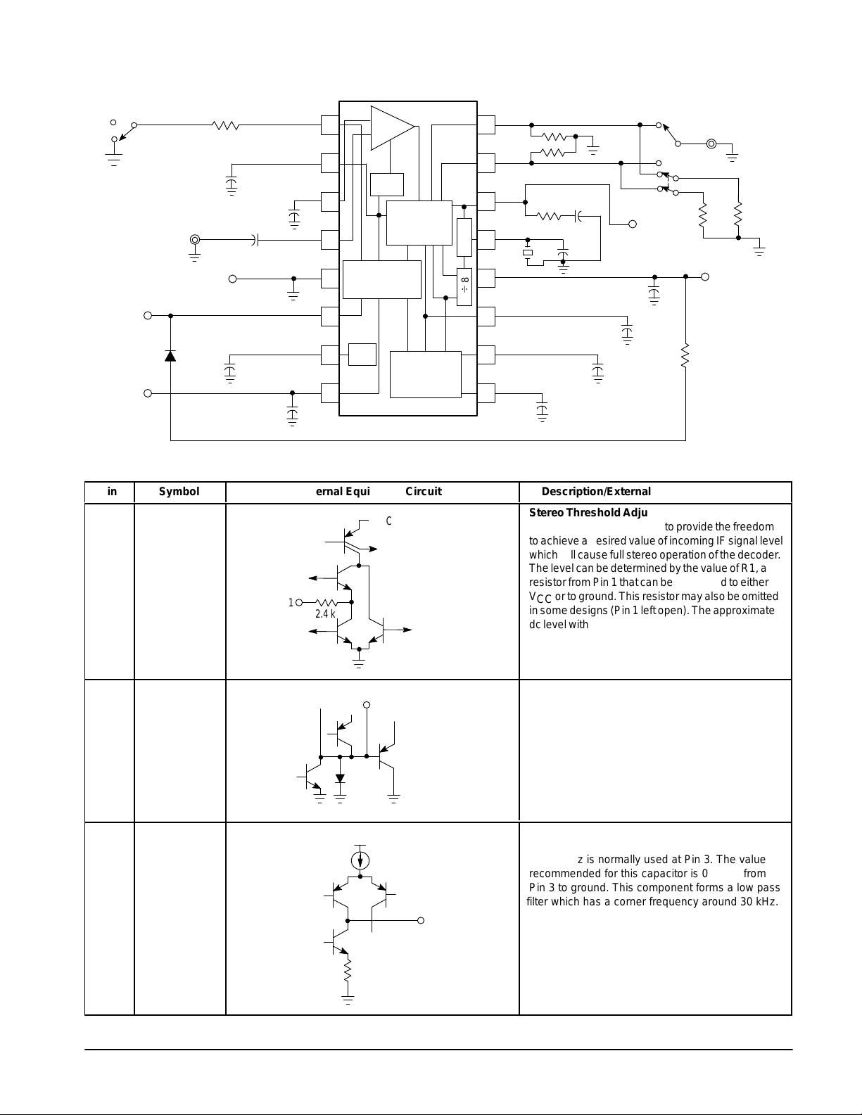
PIN FUNCTION DESCRIPTION
Internal Equivalent Circuit
V
CC
2.4 k
2
V
CC
2.0 k
Right
16
Left
15
10 k
R
O
R
O
R
L
Audio
Output
10 k
14
13
VCO
12
8
B
11
10
3.6 MHz
9
µ
10
47
µ
F
47
+
2.2 k
2.2 k
Loop
43 pF
V
+
47 µF
+
µ
F
0.22
0.47
+
F
+
µ
F
CC
2.2 k
Description/External Circuit Requirements
Stereo Threshold Adjustment Pin
The function of this circuit is to provide the freedom
ББББББББББББ
to achieve a desired value of incoming IF signal level
which will cause full stereo operation of the decoder.
ББББББББББББ
The level can be determined by the value of R1, a
ББББББББББББ
resistor from Pin 1 that can be connected to either
VCC or to ground. This resistor may also be omitted
ББББББББББББ
in some designs (Pin 1 left open). The approximate
ББББББББББББ
dc level with the pin left open is 0.6 Vdc.
ББББББББББББ
ББББББББББББ
AGC Filter Bypass Capacitor
An electrolytic capacitor is used as a bypass filter
ББББББББББББ
and it sets the time constant for the AGC circuit
ББББББББББББ
action. The recommended capacitor value is 10 µF
from Pin 2 to ground. The dc level at this pin varies
ББББББББББББ
as shown in the curve in Figure 13, AGC Voltage
versus Input Level.
ББББББББББББ
ББББББББББББ
ББББББББББББ
IF Amplifier Feedback Capacitor
ББББББББББББ
A capacitor which is specified to have a low ESR
at 450 kHz is normally used at Pin 3. The value
ББББББББББББ
recommended for this capacitor is 0.47 µF from
ББББББББББББ
Pin 3 to ground. This component forms a low pass
filter which has a corner frequency around 30 kHz.
ББББББББББББ
3
ББББББББББББ
ББББББББББББ
ББББББББББББ
ББББББББББББ
ББББББББББББ
3
Page 4
Pin
Á
Á
Á
Á
Á
Á
Á
Á
Á
Á
Á
Á
Á
Á
Á
Á
Á
Á
Á
Á
Á
Á
Á
Á
Á
Á
Á
Á
Á
Á
Á
Á
Á
Á
Á
Á
Á
Á
Á
Á
Á
Á
Á
Á
Á
Á
Á
Á
Á
Á
Á
Á
Á
Á
Á
Á
Á
Á
Á
Á
Á
Á
Á
Á
Á
Á
Á
Á
Á
Á
Á
Á
Á
Á
Á
Á
Á
Á
Á
Á
Á
Á
Á
Á
Á
Á
Á
Á
Á
Á
Á
Á
Á
Á
Á
Á
Á
Á
Á
Á
Á
Á
Á
Á
Á
Á
Á
Á
4
ÁÁ
ÁÁ
ÁÁ
ÁÁ
ÁÁ
ÁÁ
5
ÁÁ
ÁÁ
ÁÁ
ÁÁ
Symbol
IF
in
ÁÁÁ
ÁÁÁ
ÁÁÁ
ÁÁÁ
ÁÁÁ
ÁÁÁ
Gnd
ÁÁÁ
ÁÁÁ
ÁÁÁ
ÁÁÁ
MC13028A
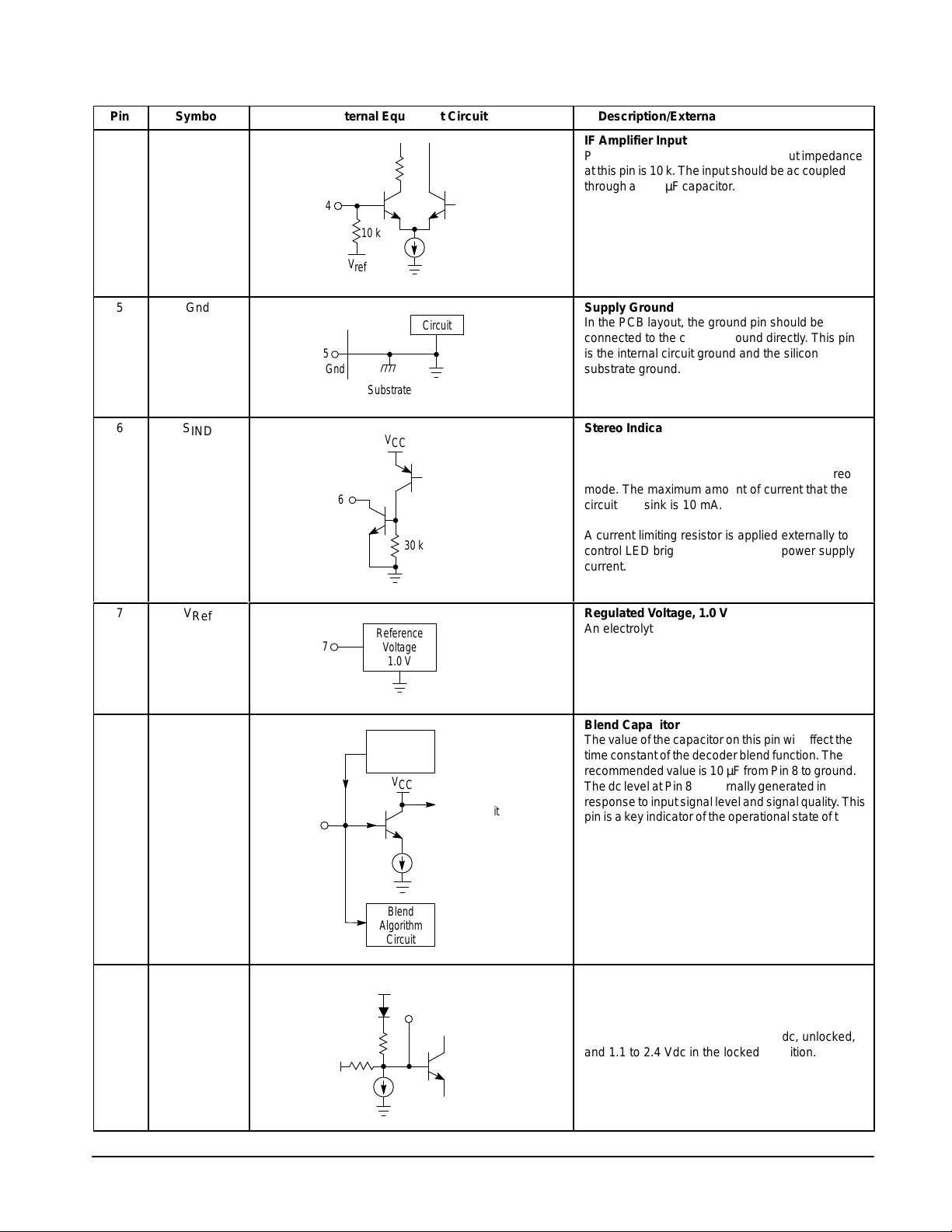
PIN FUNCTION DESCRIPTION
Internal Equivalent Circuit
БББББББББББББ
БББББББББББББ
БББББББББББББ
БББББББББББББ
БББББББББББББ
БББББББББББББ
БББББББББББББ
БББББББББББББ
БББББББББББББ
БББББББББББББ
4
5
Gnd
10 k
V
ref
Substrate
Circuit
Description/External Circuit Requirements
IF Amplifier Input
Pin 4 is the IF input pin. The typical input impedance
ББББББББББББ
at this pin is 10 k. The input should be ac coupled
ББББББББББББ
through a 0.01 µF capacitor.
ББББББББББББ
ББББББББББББ
ББББББББББББ
ББББББББББББ
Supply Ground
In the PCB layout, the ground pin should be
ББББББББББББ
connected to the chassis ground directly. This pin
ББББББББББББ
is the internal circuit ground and the silicon
substrate ground.
ББББББББББББ
ББББББББББББ
6
ÁÁ
ÁÁ
ÁÁ
ÁÁ
ÁÁ
ÁÁ
ÁÁ
7
ÁÁ
ÁÁ
ÁÁ
8
ÁÁ
ÁÁ
ÁÁ
ÁÁ
ÁÁ
ÁÁ
ÁÁ
ÁÁ
ÁÁ
ÁÁ
9
ÁÁ
ÁÁ
ÁÁ
ÁÁ
ÁÁ
ÁÁ
4
S
IND
ÁÁÁ
ÁÁÁ
ÁÁÁ
ÁÁÁ
ÁÁÁ
ÁÁÁ
ÁÁÁ
V
Ref
ÁÁÁ
ÁÁÁ
ÁÁÁ
CAP
Blend
ÁÁÁ
ÁÁÁ
ÁÁÁ
ÁÁÁ
ÁÁÁ
ÁÁÁ
ÁÁÁ
ÁÁÁ
ÁÁÁ
ÁÁÁ
I
Pilot
ÁÁÁ
ÁÁÁ
ÁÁÁ
ÁÁÁ
ÁÁÁ
ÁÁÁ
V
43 k
CC
30 k
Reference
Voltage
1.0 V
Blend Cap
Charging
Circuit
V
CC
Blend
Algorithm
Circuit
V
CC
9
Pilot Indicator
Driver Circuit
БББББББББББББ
БББББББББББББ
БББББББББББББ
БББББББББББББ
БББББББББББББ
БББББББББББББ
БББББББББББББ
БББББББББББББ
БББББББББББББ
БББББББББББББ
БББББББББББББ
БББББББББББББ
БББББББББББББ
БББББББББББББ
БББББББББББББ
БББББББББББББ
БББББББББББББ
БББББББББББББ
БББББББББББББ
БББББББББББББ
БББББББББББББ
БББББББББББББ
БББББББББББББ
БББББББББББББ
БББББББББББББ
БББББББББББББ
6
7
8
V
reg
Stereo Indicator Driver
This driver circuit is intended to light an LED or
ББББББББББББ
other indicator when the decoder receives the
ББББББББББББ
proper input signals and switches into the stereo
mode. The maximum amount of current that the
ББББББББББББ
circuit can sink is 10 mA.
ББББББББББББ
A current limiting resistor is applied externally to
ББББББББББББ
control LED brightness versus total power supply
current.
ББББББББББББ
ББББББББББББ
Regulated Voltage, 1.0 V
An electrolytic capacitor used as a bypass filter is
ББББББББББББ
recommended from Pin 7 to ground. The capacitor
value should be 10 µF.
ББББББББББББ
ББББББББББББ
Blend Capacitor
ББББББББББББ
The value of the capacitor on this pin will effect the
time constant of the decoder blend function. The
ББББББББББББ
recommended value is 10 µF from Pin 8 to ground.
ББББББББББББ
The dc level at Pin 8 is internally generated in
response to input signal level and signal quality. This
ББББББББББББ
pin is a key indicator of the operational state of the IC
ББББББББББББ
(see text Functional Description). It is recommended
to discharge the blend capacitor externally when
ББББББББББББ
changing stations.
ББББББББББББ
ББББББББББББ
ББББББББББББ
ББББББББББББ
Pilot I Detector Output
The Pilot I Detector output requires a 10 µF
ББББББББББББ
electrolytic capacitor to ground. The value of this
capacitor sets the pilot acquisition time. The dc
ББББББББББББ
level at Pin 9 is approximately 1.0 Vdc, unlocked,
ББББББББББББ
and 1.1 to 2.4 Vdc in the locked condition.
ББББББББББББ
ББББББББББББ
ББББББББББББ
MOTOROLA ANALOG IC DEVICE DATA
Page 5
Pin
Á
Á
Á
Á
Á
Á
Á
Á
Á
Á
Á
Á
Á
Á
Á
Á
Á
Á
Á
Á
Á
Á
Á
Á
Á
Á
Á
Á
Á
Á
Á
Á
Á
Á
Á
Á
Á
Á
Á
Á
Á
Á
Á
Á
Á
Á
Á
Á
Á
Á
Á
Á
Á
Á
Á
Á
Á
Á
Á
Á
Á
Á
Á
Á
Á
Á
Á
Á
Á
Á
Á
Á
Á
Á
Á
Á
Á
Á
Á
Á
Á
Á
Á
Á
Á
Á
Á
Á
Á
Á
Á
Á
Á
10
ÁÁ
ÁÁ
ÁÁ
ÁÁ
ÁÁ
ÁÁ
ÁÁ
ÁÁ
11
ÁÁ
ÁÁ
ÁÁ
ÁÁ
ÁÁ
ÁÁ
ÁÁ
ÁÁ
ÁÁ
12
ÁÁ
ÁÁ
ÁÁ
ÁÁ
ÁÁ
Symbol
Q
Pilot
ÁÁÁ
ÁÁÁ
ÁÁÁ
ÁÁÁ
ÁÁÁ
ÁÁÁ
ÁÁÁ
ÁÁÁ
PILOT
fil
ÁÁÁ
ÁÁÁ
ÁÁÁ
ÁÁÁ
ÁÁÁ
ÁÁÁ
ÁÁÁ
ÁÁÁ
ÁÁÁ
V
CC
ÁÁÁ
ÁÁÁ
ÁÁÁ
ÁÁÁ
ÁÁÁ
MC13028A
PIN FUNCTION DESCRIPTION
Internal Equivalent Circuit
5.0 k
30 k
V
10
CC
V
V
CC
CC
2.0 k
V
CC
12
V
CC
БББББББББББББ
БББББББББББББ
БББББББББББББ
БББББББББББББ
БББББББББББББ
БББББББББББББ
БББББББББББББ
БББББББББББББ
БББББББББББББ
БББББББББББББ
БББББББББББББ
БББББББББББББ
11
БББББББББББББ
БББББББББББББ
БББББББББББББ
БББББББББББББ
БББББББББББББ
БББББББББББББ
БББББББББББББ
БББББББББББББ
БББББББББББББ
БББББББББББББ
Description/External Circuit Requirements
Pilot Q Detector Output
ББББББББББББ
This pin is connected to the Pilot Q detector and
requires a 0.47 µF capacitor to ground to filter the
ББББББББББББ
error line voltage at the PLL pilot tone detector. If the
ББББББББББББ
value of this capacitor is made too large, the
decoder may be prevented from coming back into
ББББББББББББ
stereo after a signal drop out has been experienced
in the field. The force to mono function is also
ББББББББББББ
accomplished at this pin by pulling the dc voltage
ББББББББББББ
level at the pin below 1.0 V.
ББББББББББББ
ББББББББББББ
Pilot Signal Input
ББББББББББББ
A capacitor to ground forms a filter for the pilot input
signal. The recommended value of the capacitor is
ББББББББББББ
0.22 µF . The dc level at Pin 1 1 is approximately
ББББББББББББ
1.0 Vdc.
ББББББББББББ
ББББББББББББ
ББББББББББББ
ББББББББББББ
ББББББББББББ
ББББББББББББ
Supply Voltage (VCC)
The operating supply voltage range is from 1.8 Vdc
ББББББББББББ
to 12 Vdc.
ББББББББББББ
ББББББББББББ
ББББББББББББ
ББББББББББББ
13
ÁÁ
ÁÁ
ÁÁ
ÁÁ
ÁÁ
ÁÁ
ÁÁ
ÁÁ
ÁÁ
ÁÁ
MOTOROLA ANALOG IC DEVICE DATA
OSC
in
ÁÁÁ
ÁÁÁ
ÁÁÁ
ÁÁÁ
ÁÁÁ
ÁÁÁ
ÁÁÁ
ÁÁÁ
ÁÁÁ
ÁÁÁ
БББББББББББББ
БББББББББББББ
БББББББББББББ
БББББББББББББ
БББББББББББББ
БББББББББББББ
БББББББББББББ
БББББББББББББ
БББББББББББББ
БББББББББББББ
2.2 k
V
13
V
reg
reg
3.1 k
3.0 k
6.3 pF
15 k
Oscillator Input
The oscillator pin requires a ceramic resonator and
ББББББББББББ
parallel capacitor connected to ground. The
ББББББББББББ
recommended source for the ceramic resonator is
Murata, part number CSA 3.60MGF108.
ББББББББББББ
A 43 pF NPO capacitor is in parallel with the
resonator. The dc level at Pin 13 is approximately
ББББББББББББ
1.1 Vdc.
ББББББББББББ
ББББББББББББ
ББББББББББББ
ББББББББББББ
ББББББББББББ
ББББББББББББ
5
Page 6
Pin
Á
Á
Á
Á
Á
Á
Á
Á
Á
Á
Á
Á
Á
Á
Á
Á
Á
Á
Á
Á
Á
Á
Á
Á
Á
Á
Á
Á
Á
Á
Á
Á
Á
Á
Á
Á
Á
Á
Á
Á
Á
Á
Á
Á
Á
Á
Á
Á
Á
Á
Á
Á
Á
Á
Á
Á
Á
Á
Á
Á
Á
Á
Á
Á
Á
Á
Á
Á
Á
Á
Á
Á
Á
Á
Á
Á
Á
Á
Á
Á
Á
14
ÁÁ
ÁÁ
ÁÁ
ÁÁ
ÁÁ
ÁÁ
ÁÁ
ÁÁ
ÁÁ
ÁÁ
ÁÁ
Symbol
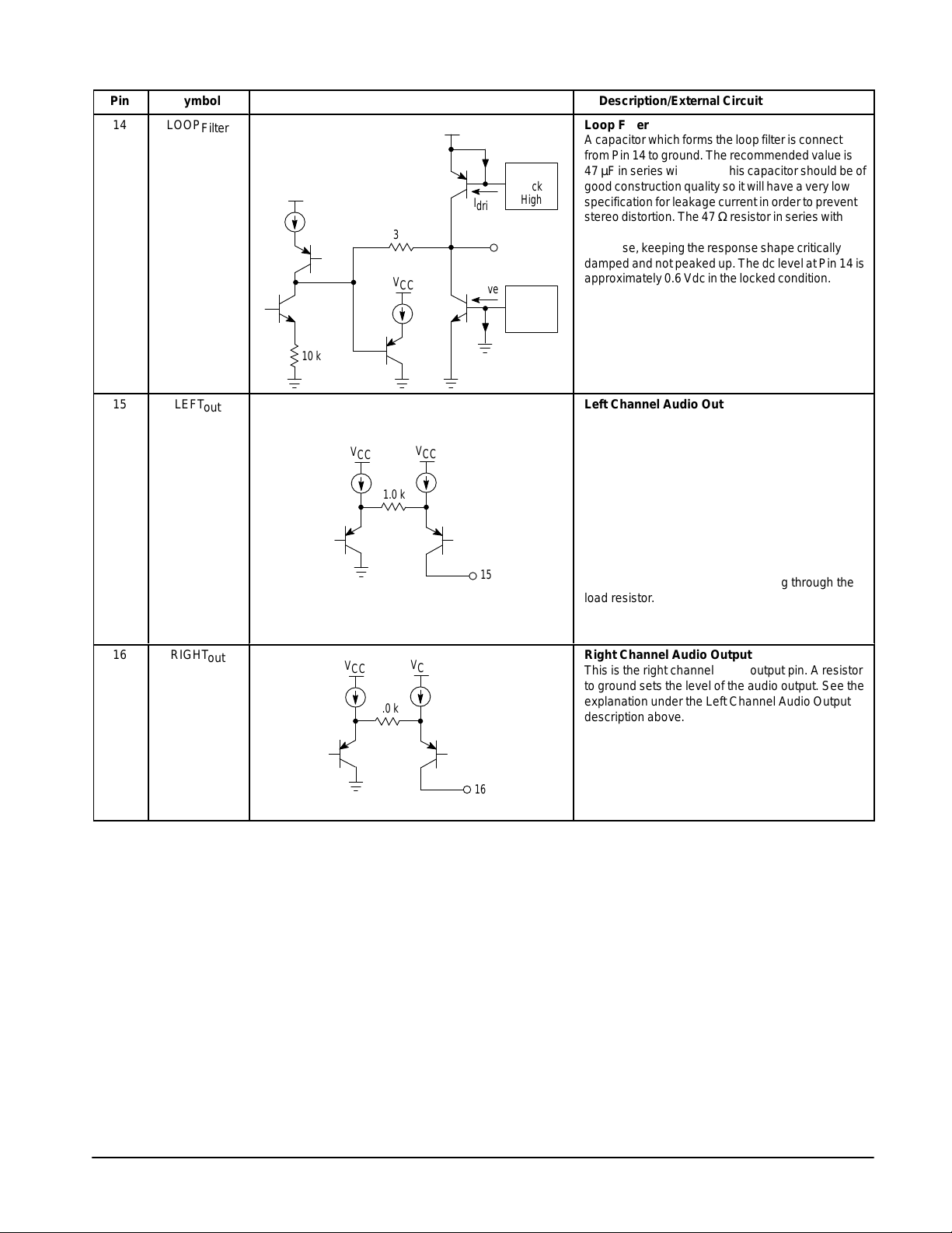
LOOP
Filter
ÁÁÁ
ÁÁÁ
ÁÁÁ
ÁÁÁ
ÁÁÁ
ÁÁÁ
ÁÁÁ
ÁÁÁ
ÁÁÁ
ÁÁÁ
ÁÁÁ
MC13028A
PIN FUNCTION DESCRIPTION
Internal Equivalent Circuit
V
БББББББББББББ
БББББББББББББ
БББББББББББББ
V
CC
БББББББББББББ
БББББББББББББ
БББББББББББББ
БББББББББББББ
БББББББББББББ
БББББББББББББ
БББББББББББББ
10 k
БББББББББББББ
390
V
CC
CC
I
drive
I
drive
Fast
Lock
High
14
Fast
Lock
Low
Description/External Circuit Requirements
Loop Filter
ББББББББББББ
A capacitor which forms the loop filter is connected
from Pin 14 to ground. The recommended value is
ББББББББББББ
47 µF in series with 47 Ω. This capacitor should be of
ББББББББББББ
good construction quality so it will have a very low
specification for leakage current in order to prevent
ББББББББББББ
stereo distortion. The 47 Ω resistor in series with the
capacitor controls the PLL corner frequency
ББББББББББББ
response, keeping the response shape critically
ББББББББББББ
damped and not peaked up. The dc level at Pin 14 is
approximately 0.6 Vdc in the locked condition.
ББББББББББББ
ББББББББББББ
ББББББББББББ
ББББББББББББ
ББББББББББББ
15
ÁÁ
ÁÁ
ÁÁ
ÁÁ
ÁÁ
ÁÁ
ÁÁ
ÁÁ
ÁÁ
ÁÁ
16
ÁÁ
ÁÁ
ÁÁ
ÁÁ
ÁÁ
ÁÁ
ÁÁ
LEFT
out
ÁÁÁ
ÁÁÁ
ÁÁÁ
ÁÁÁ
ÁÁÁ
ÁÁÁ
ÁÁÁ
ÁÁÁ
ÁÁÁ
ÁÁÁ
RIGHT
out
ÁÁÁ
ÁÁÁ
ÁÁÁ
ÁÁÁ
ÁÁÁ
ÁÁÁ
ÁÁÁ
БББББББББББББ
БББББББББББББ
БББББББББББББ
БББББББББББББ
БББББББББББББ
БББББББББББББ
БББББББББББББ
БББББББББББББ
БББББББББББББ
БББББББББББББ
БББББББББББББ
БББББББББББББ
БББББББББББББ
БББББББББББББ
БББББББББББББ
БББББББББББББ
БББББББББББББ
V
CC
V
CC
1.0 k
1.0 k
V
CC
15
V
CC
16
Left Channel Audio Output
This is the left channel audio output pin from which
ББББББББББББ
the IC can provide 1.3 µApp drive current for each
ББББББББББББ
percent of mono modulation. A resistor to ground
sets the level of the audio output.
ББББББББББББ
For example,
ББББББББББББ
drive per % mod) = 130 µApp flowing through the
ББББББББББББ
load resistor. (For a 2.2 k load, 286 mVpp is then
the output signal voltage.) When dealing with
ББББББББББББ
stereo signals, multiply the mod level by 2; i.e.
(left only mod) x 2 (stereo factor) x 1.3 µApp (IC
ББББББББББББ
drive per % mod) = 130 µApp flowing through the
ББББББББББББ
load resistor.
ББББББББББББ
ББББББББББББ
Right Channel Audio Output
ББББББББББББ
This is the right channel audio output pin. A resistor
to ground sets the level of the audio output. See the
ББББББББББББ
explanation under the Left Channel Audio Output
ББББББББББББ
description above.
ББББББББББББ
ББББББББББББ
ББББББББББББ
ББББББББББББ
100%
(mono mod) x 1.3 µApp (IC
50%
6
MOTOROLA ANALOG IC DEVICE DATA
Page 7

MC13028A
Figure 1. T ypical Circuit for E.T.R. Applications
Right Output
Left Output
RF AGC’d IF Signal from
Mixer (450 kHz from
Tuner IC Section)
Threshold Adjust
NRSC Roll–Off Filter
16 15 14 13 12 11 10 9
IF
Amp
Stereo
12345678
R1
10
R
O
R
O
+
µ
F
47
(Note 1)
47
AM Stereo
Decoder
AGC
AGC
BypassIFBypass
+
µ
F 0.01 µF
+
0.47 µF
(Note 5)
(Note 2)
(Note 3)
VCO
IF
Input
V
CC
0.22
(Note 4)
43 pF
B
8
Signal Quality
Detector
Gnd Stereo
µ
F
Pilot
Input
Indicator
0.47
10
µ
F
++
Pilot Q
Input
Pilot Tone
Detector
Reg
Ref
++
10 µF
10
µ
F
µ
F
Pilot I
Input
Blend
(Note 6)
+
47 µF
Optional
Force to
Mono
Scan
Mute
NOTES: 1. The 47 µF capacitor is recommended to be a low leakage type capacitor. Leakage current due to this capacitor causes
increase in stereo distortion and decreased separation performance.
2.The recommended source for this part is Murata Products. CSA3.60MGF108. The location of this part should be carefully
considered during the layout of the decoder circuit. This part should not be near the audio signal paths, the 25 Hz pilot filter
lines, or the VCC high current lines, and the ceramic element ground line should be direct to the chassis ground lead in order
to avoid any oscillator inter–modulation.
3.The 43 pF capacitor is recommended to be a NPO type ceramic part. Changing the value of this capacitor alters the lock
range of the decoder PLL.
4.The tolerance on the value of the 0.22 µF capacitor should be within ±20% for the full design temperature range of operation.
Any reduction in the value of this capacitor due to temperature excursions will reduce the pilot tone circuit sensitivity.
5.The 0.47 µF capacitor is recommended to be a low ESR type capacitor, (less than 1.5 Ω) in order to avoid increased audio
output distortions under weak input signal conditions with higher modulation levels.
6.The scan/mute function is located on the Blend pin at Pin 8. To provide this function, Pin 8 should be pulled down below 0.3 V
until the decoder and the synthesizer have both locked to a new station.
MOTOROLA ANALOG IC DEVICE DATA
7
Page 8

MC13028A
FUNCTIONAL DESCRIPTION
Introduction
The MC13028A is designed as a low voltage, low cost
decoder for the C–QUAM AM Stereo technology and is
completely compatible with existing monaural AM
transmissions. The IC requires relatively few, inexpensive
external parts to produce a full featured C–QUAM AM Stereo
implementation. The layout is straightforward and should
produce excellent stereo performance. This device performs
the function of IF amplification, AGC, modulation detection,
pilot tone detection, signal quality inspection, and left and
right audio output matrix operation. The IC is targeted for use
in portable and home AM Stereo radio applications.
A simple overview follows which traces the path of the
input signal information to the MC13028A all the way to the
audio output pins of the decoder IC.
From the appropriate pin of an AM IC, the IF amplifier
circuit of the MC13028A receives its input at Pin 4 as a
450 kHz, typically modulated C–QUAM signal. The input
signal level for stereo operation can vary from 47 dBµV to
about 90 dBµV. A specific threshold level between these
limits can be designed into a receiver by the choice of the
resistor value for R1 connected to Pin 1. This IC design
incorporates feedback in the IF circuit section which provides
excellent dc balance in the IF amplifier. This balanced
condition also guarantees excellent monophonic
performance from the decoder. An IF feedback filter at Pin 3
is formed by a 0.47 µF low leakage capacitor. It is used to
filter out the unwanted audio which is present on the IF
amplifier feedback line at higher modulation levels under
weak input RF signal conditions. Elimination of the unwanted
signal helps to decrease the amount of distortion in the audio
output of the stereo decoder under these particular input
conditions. An AGC circuit controls the level of IF signal
which is subsequently fed to the detector circuits. An AGC
bypass capacitor is connected to Pin 2 and forms a single
pole low pass filter. The value of this part also sets the time
constant for the AGC circuit action.
The amplified C–QUAM IF signal is fed simultaneously to
the envelope detector circuit, and to a C–QUAM converter
circuit. The envelope detector provides the L+R (mono)
signal output which is fed to the stereo matrix. In the
converter circuit, the C–QUAM signal is restored to a Quam
signal. This is accomplished by dividing the C–QUAM IF
signal by the demodulated cos φ term. The cos φ term is
derived from the phase modulated IF signal in an active
feedback loop. Cosine φ is detected by comparing the
envelope detector and the in–phase detector outputs in the
high speed comparator/feedback loop. Cosine φ is extracted
from the I detector output and is actively transferred through
feedback to the output of the comparator. The output of the
comparator is in turn fed to the control input of the divider,
thus closing the feedback loop of the converter circuit. In this
process, the cos φ term is removed from the divider IF output,
thus allowing direct detection of the L–R by the quadrature
detector. The audio outputs from both the envelope and the
L–R detectors are first filtered to minimize the second
harmonic of the IF signal. Then they are fed into a matrix
circuit where the Left channel and the Right channel outputs
can be extracted at Pins 15 and 16. (The outputs from the I
and Q detectors are also filtered similarly.) At this time, a
stereo indicator driver circuit, which can sink up to 10 mA, is
also enabled. The stereo output will occur if the input IF
signal is: larger than the stereo threshold level, not too noisy ,
and if a proper pilot tone is present. If these three conditions
are not met, the blend circuit will begin to force monaural
operation at that time.
A blend circuit is included in this design because
conditions occur during field use that can cause input signal
strength fluctuation, strong unwanted co–channel or power
line interference, and/or multi–path or re–radiation. When
these aberrant conditions occur, rapid switching between
stereo and mono might occur, or the stereo quality might be
degraded enough to sound displeasing. Since these
conditions could be annoying to the normal listener, the
stereo information is blended towards a monaural output.
This circuit action creates a condition for listening where
these aberrant effects are better tolerated by the consumer .
Intentional mono operation is a feature sometimes
required in receiver designs. There are several ways in which
to accomplish this feat. First, a resistor from Pin 10 to ground
can be switched into the circuit. A value of 1.0 k is adequate
as is shown in the schematic in Figure 18. A second method
to force the decoder into mono is simply to shunt Pin 10 to
ground through an NPN transistor (collector to Pin 10, emitter
to ground), where the base lead is held electrically “high” to
initiate the action.
A third method to force a mono condition upon the
decoder is to shunt Pin 8 of the decoder to ground through
an NPN transistor as described above. Effectively, this
operation discharges the blend capacitor (10 µF), and the
blend function takes over internally forcing the decoder into
mono. This third method does not necessarily require extra
specific parts for the forced mono function as the first two
examples do. The reason for this is that most electronically
tuned receiver designs require an audio muting function
during turn on/turn off, tuning/scanning, or band switching
(FM to AM). When the muting function is designed into an
AM Stereo receiver, it also should include a blend capacitor
reset (discharge) function which is accomplished in this case
by the use of an NPN transistor shunting Pin 8 to ground,
(thus making the addition of a forced mono function almost
“free”). The purpose of the blend reset during muting is to
re–initialize the decoder back into the “fast lock” mode from
which stereo operation can be attained much quicker after
any of the interruptive activities mentioned earlier, (i.e. turn
on, tuning, etc.).
The VCO in this IC is a phase shift oscillator type design
that operates with a ceramic resonator at eight times the IF
frequency, or 3.60 MHz. With IF input levels below the
stereo threshold level, the oscillator is not operational. This
feature helps to eliminate audio tweets under low level,
noisy input conditions.
8
MOTOROLA ANALOG IC DEVICE DATA
Page 9

MC13028A
The phase locked loop (PLL) in the MC13028A is locked to
the L–R signal. This insures good stereo distortion
performance at the higher levels of left only or right only
modulations. Under normal operating conditions, the PLL
remains locked because of the current flow capability of the
loop driver circuit. This high gain, high impedance circuit
performs optimally when the current flow is balanced. The
balanced condition is enhanced by the loop driver filter circuit
connected between Pin 14 and ground. The filter circuit
consists of a 47 Ω resistor in series with a 47 µF capacitor. The
47 Ω resistor is to set the Fast Lock rate. It is recommended
that the capacitor be a very low leakage type electrolytic, or a
tantalum composition part because any significant amount of
leakage current flowing through the capacitor will unbalance
the loop driver circuit and result in less than optimum stereo
performance, see Figures 10 and 11.
The pilot tone detector circuit is fed internally from the Q
detector output signal. The circuit input employs a low pass
filter at Pin 11 that is designed to prevent the pilot tone
detector input from being overloaded by higher levels of L–R
modulation. The filter is formed by a 0.22 µF capacitor and
the input impedance of the first amplifier. A pilot I detector
DISCUSSION OF GRAPHS AND FIGURES
If the general recommendations put forth in this application
guide are followed, excellent stereo performance should
result.
The curves in Figures 2 through 7 depict the separation
and the distortion performance in stereo for 30%, 50%, and
65% single channel modulations respectively. The data for
these figures were collected under the conditions of
VCC = 8.0 V and RO = 10 k in both the left and the right
channels as applied to the application circuit of Figure 1. A
very precise laboratory generator was used to produce the
AM Stereo test signal of 450 kHz at 70 dBµV fed to Pin 4. An
NRSC post detection filter was not present at the time of
these measurements. The audio separation shows an
average performance at 30% and 50% modulations of
– 45 dB in the frequency range of 2.0 kHz to 5.0 kHz. The
corresponding audio distortions under these conditions are
about 0.28% at 30% modulation, and about 0.41% at 50%
modulation.
Figure 6 shows that the typical separation at 65%
modulation in the 2.0 kHz to 5.0 kHz region is about –37 dB,
and the corresponding audio distortion shown in Figure 7 is
about 1.0%. The performance level of these sinusoidal
signals is somewhat less than those discussed in the
circuit employs a capacitor to ground at Pin 9 to operate in
conjunction with an internal resistor to create an RC
integration time. The value of the capacitor determines the
amount of time required to produce a stereo indication. This
amount must include the time it takes to check for the
presence of detector falsing due to noise or interference,
station retuning by the customer, and pilot dropout in the
presence of heavy interference. The pilot Q detector utilizes
a filter on its pilot tone PLL error line at Pin 10. This capacitor
to ground (usually 0.47 µF) is present to filter any low
frequency L–R information that may be present on the error
line. If the value of this capacitor is allowed to be too small,
L–R modulation ripple on the error line may get large enough
to cause stereo dropout. If the capacitor value is made too
large, the pilot tone may be prevented from being reacquired
if it is somehow lost due to fluctuating field conditions.
A 1.0 V reference level is created internally from the V
source to the IC. This regulated line is used extensively by
circuits throughout the MC13028A design. An electrolytic
capacitor from Pin 7 to ground is used as a filter for the
reference voltage.
previous paragraph due to the internal operation of the
clamping circuits. In the field, the transmitters at AM Stereo
radio stations are not usually permitted to modulate single
channel levels past 70%. Therefore these conditions do not
occur very often during normal broadcast material.
The roll–off at both the low and high frequencies of the
30% single channel driven responses is due to the fact that a
post detection bandpass filter of 60 Hz to 10 kHz was used in
the measurement of the data, while a post detection filter of
2.0 Hz to 20 kHz was used for the collection of data in the
50% and 65% modulation examples. The tighter bandwidth
was used while collecting the performance data at 30%
modulation levels in order to assure that the distortion
measurement was indicative of the true distortion products
measured near the noise floor and thus not encumbered by
residual noise and hum levels which would erroneously add
to the magnitude of the harmonic distortion data. Note in
Figure 8 the traces of noise response for the four different
bandwidths of post detection filtering. It can be seen that the
noise floors improve steadily with increasing levels of
incoming 450 kHz as the value of the lower corner frequency
of the filter is increased. Data for the stereo noise floors was
collected with the decoder in the forced stereo mode.
CC
MOTOROLA ANALOG IC DEVICE DATA
9
Page 10

MC13028A
0
–10
–20
–30
SEPARATION (dB)
–40
–50
0
–10
Figure 2. Single Channel Separation
at 30% Modulation
Desired Channel
See Text
Undesired Channel
100
f, FREQUENCY (Hz)
1.0 k 10 k 1.0 k 10 k
Figure 4. Single Channel Separation
at 50% Modulation
Desired Channel
10
1.0
DISTORTION (%)
0.1
10
Figure 3. Single Channel Distortion
at 30% Modulation
100
f, FREQUENCY (Hz)
Figure 5. Single Channel Distortion
at 50% Modulation
–20
–30
SEPARATION (dB)
–40
–50
0
–10
–20
–30
SEPARATION (dB)
–40
Undesired Channel
100
f, FREQUENCY (Hz)
1.0 k 10 k 1.0 k 10 k
Figure 6. Single Channel Separation
at 65% Modulation
Desired Channel
Undesired Channel
1.0
DISTORTION (%)
0.1
10
1.0
DISTORTION (%)
100
f, FREQUENCY (Hz)
Figure 7. Single Channel Distortion
at 65% Modulation
10
–50
100
0.1
f, FREQUENCY (Hz) f, FREQUENCY (Hz)
100
1.0 k 10 k1.0 k 10 k
MOTOROLA ANALOG IC DEVICE DATA
Page 11

Figure 8. Stereo Noise and Stereo Composite
Distortion when Mono Transmitted
10
0
–10
Stereo Audio Level
Stereo Composite Distortion
MC13028A
7.0
6.0
5.0
Figure 9. R1 versus Stereo Threshold Point
1000
R1 to V
CC
–20
Noise
5.0 Hz to 3.0 kHz
–30
–40
–50
RESPONSE FOR 30%, MONO MODULATION (dB)
40
50 Hz to 3.0 kHz
50 60 70 80 48 50 60
SIGNAL STRENGTH (dBµV)
100 Hz to 3.0 kHz
Figure 10. Decoder Separation versus Filter
Capacitor (Pin 14) Leakage Current
50
45
40
35
SEPARATION (dB)
30
25
400 Hz to 3.0 kHz
4.0
3.0
2.0
1.0
0
DISTORTION FOR 80% MONO MODULATION (%)
Ω
100
R1 (k )
R1 to Gnd
10–60
46
52 54 56 58
STEREO THRESHOLD (dB
Figure 11. Decoder Distortion versus Filter
Capacitor (Pin 14) Leakage Current
2.0
1.0
µ
V)
20
– 600
– 400 – 400
Figure 12. Low Frequency Corner
4.0
Loop Filter 47 µF
0
– 4.0
– 8.0
PLL LOOP RESPONSE (dB)
10
– 200 0 200 400 600 – 200 0 200 400 600
LEAKAGE CURRENT (10–9)
DISTORTION, 50% SINGLE CHANNEL MOD
– 600
LEAKAGE CURRENT (10–9)
Figure 13. AGC Voltage versus
of PLL Response
Loop Filter 15 µF
MODULA TION FREQUENCY (Hz)
Loop Filter 4.7 µF
100
500
400
300
200
AGC VOLTAGE LEVEL (mV)
100
0–12
40
Input Signal Level
50 60 70 80
INPUT SIGNAL STRENGTH (dB
90
µ
V)
MOTOROLA ANALOG IC DEVICE DATA
11
Page 12

MC13028A
Figure 9 presents more detailed information with respect
to the value of resistor R1 at Pin 1 versus the desired
incoming signal level for stereo threshold.
Figures 10 and 11, discussed briefly in the Pin Function
Description Section, show the importance of using a quality
component at Pin 14 to ground. It can be seen that an
electrolytic capacitor leakage current of 600 nA can
unbalance the PLL to the point where stereo performance
may degrade to only 25 dB of separation with a
corresponding 2.0% distortion at 50% modulation levels.
The value of the capacitor connected to Pin 14 (47 µF) is
also a factor in the determination of the low frequency corner
of the PLL circuit response. Three traces of PLL response
appear in Figure 12 where they have been plotted for three
different values of loop filter capacitor. The recommended
value of 47 µF provides the best response shape in this
particular circuit set–up where a Murata Products
CSA3.60MGF108 part is used.
AM STEREO TUNER / FM STEREO IF
Description of Application
This application combines a Sanyo LA1832M with the
Motorola MC13028A AM Stereo decoder IC. The LA1832
provides an FM IF, FM multiplex detection, AM tuning, and
the AM IF functions. The MC13028A provides the AM Stereo
detection as well as Left and Right audio outputs. An
MC145151 synthesizer provides the frequency control of the
local oscillator contained within the LA1832. Frequency
selection is by means of a switch array attached to the
synthesizer. The application circuit is shown in Figure 18.
Circuit Board Description
The copper side layout and the component locations are
shown in Figure 19. The view is from the plating side of the
board, with the components shown in hidden view. Several
jumper wires are placed on the component side of the board
to complete the circuit. Posts are provided for electrical
connections to the circuit. The circuit board has been scaled
to fit the page, however, the dimensions provide the true size.
Circuit Description
The Sanyo data sheet for the LA1832 should be
consulted for an understanding of the FM detection and
multiplex decoding.
Figure 13 presents the response of the AGC voltage
versus decoder input signal level. This is a typical response
when the IC is used as shown in the application schematic of
Figure 1. The trace begins approximately at the point of
decoder sensitivity, and rises rapidly until reaching the area
of stereo sensitivity, approximately 50 dBµV. Thereafter, the
circuit responds in a linear fashion for the next 30 dB of input
signal increase.
Figures 14 through 17 inclusively depict the VCC ripple
rejection performance for the MC13028A under mono and
stereo conditions for nominal and for low values of VCC. It
should be noted that this data was collected without any V
filtering. As one might expect, the ripple rejection is better in
mono than in stereo. When the decoder operates in stereo,
the VCO is functional, thus the decoder becomes more
susceptible to audio ripple on the VCC line. Under normal
operating conditions, with the recommended value of 47 µF
at Pin 12 and 10 µF at Pin 7, a VCC ripple reading will be
virtually the same as measuring the noise floor of the IC.
Special Parts
The following information provides circuit function, part
number, and the manufacturer’s name for special parts
identified by their schematic symbol. Where the part is not
limited to a single source, a description sufficient to select a
part is given.
U1 IC – AM Stereo Decoder
MC13028AD by Motorola
U2 IC – AM/FM IF and Multiplex Tuner
LA1832M by Sanyo
U3 IC – Frequency Synthesizer
MC145151DW2 by Motorola
T1 AM IF Coil
A7NRES–11148N by TOKO
F1 AM IF Ceramic Filter
SFG450F by Murata
F2 FM IF Detector Resonator
CDA10.7MG46A by Murata
F3 FM Multiplex Decoder Resonator
CSB456F15 by Murata
F4 AM Tuner Block
BL–70 by Korin Giken
X1 10.24 MHz Crystal, Fundamental Mode,
A T Cut, 18 pF Load Cap, 35 Ω maximum series R.
HC–18/U Holder
X2 3.6 MHz AM Stereo Decoder Resonator
CSA3.60MGF108 by Murata
S5 8 SPST DIP Switch
CC
12
MOTOROLA ANALOG IC DEVICE DATA
Page 13

–20
–30
–40
RESIDUAL (dB)
–50
Figure 14. Mono VCC Ripple Rejection
µ
F
300
100 mV
pp
VCC = 4.0 V
VCC = 6.0 V
VCC = 8.0 V
VCC = 10 V
VCC = 12 V
50
V
CC
Decoder
10 k 10 k
MC13028A
L
R
–20
–30
–40
RESIDUAL (dB)
–50
Figure 15. Mono Low Voltage
VCC Ripple Rejection
VCC = 3.0 V
VCC = 4.0 V
VCC = 2.0 V
VCC = 2.1 V
VCC = 2.5 V
–60
–20
–30
–40
RESIDUAL (dB)
–50
–60
Figure 16. Stereo VCC Ripple Rejection
300
µ
VCC = 4.0 V
100 mV
VCC = 8.0 V
VCC = 10 V
VCC = 12 V
100
F
pp
Decoder
50
V
CC
VCC = 6.0 V
10 k 10 k
–60
100
1.0 k100 1.0 k
RIPPLE FREQUENCY (Hz)RIPPLE FREQUENCY (Hz)
Figure 17. Stereo Low Voltage
VCC Ripple Rejection
0
L
R
–20
–30
RESIDUAL (dB)
–40
–50
–60
–10
VCC = 3.0 V
VCC = 4.0 V
100
VCC = 2.0 V
VCC = 2.5 V
1.0 k1.0 k
RIPPLE FREQUENCY (Hz)RIPPLE FREQUENCY (Hz)
MOTOROLA ANALOG IC DEVICE DATA
13
Page 14

MC13028A
Figure 18. MC13028A Decoder IC Application
Left
F
µ
C20
Figure 18. MC13028A Decoder IC Application
10
C39
R14
Stereo Tuning
F
µ
1.0
C14
R3
C6
C5 0.1
C41
0.001
6.81 k
F
µ
47
10.2 k
R15
3.01 k
F
µ
C34
2.2
Stereo
F
µ
10
AM Audio
F
µ
C19
10
16151413121110
1234567
MC13028A
F
µ
C10
10
392
R18
D2 D3
C30
12
R17
43 k
F
µ
1.0
C25
S2
AM
FM
Mono
FM S3
C43
0.01
F
µ
C42
10
Left
Right
FM Audio
Right
C13
R2
F
µ
C11
0.47
F2
R20
1.0 k
1.0 k
R19
C44
0.001
6.81 k
CDA10.7
LA1832M
0.01
C4
R40
47.5
U1
Murata
MG46A
121110
131415161718192021
F3
F
µ
47
43
C9
3.6 MHz
X2
C30.22
Mono
AM
C2
0.47
F
9
µ
C1
10
F
µ
8
C22
10
F
µ
C23
10
C12 0.01
9876543
U2
F
µ
22
0.047
0.0047
0.0012
F
µ
C40
1.0
C37 C35 C36
C38
R36
1.0 k
S4 Stereo
2
222324
Korin Giken
BL-70 Ant. Tuning Block
6
1
CC
V
C34
C49
TOKO
F4
C4810C47
68
U3
A7NRES–11148N
450 kHz IF
C52
F
µ
C53
100
F
µ
2.2
D7
1N4148
0.01
C8
0.1
X1
F
C7
µ
100
MC145151DW
T1
1
C29
0.01
R34
R39
3
12
Input
AM Ant.
10.24 MHz
28272625242322212019181716
2345678
1
SFG450F
Murata
F1
4
3
2
0.047
C27
F
µ
C28
10 k
10
3.32 k
4
L.O.
5
6
C57
R29
30 VAR
10
9
127
15
1011121314
2N3904
Q3
392
R26
332
R30
Q4
2N3906
C26
0.047
301
R25
R21
51.1
Input
FM IF
12 3
R24
R28
2.74 k
3.65 k
Q2
R35
4
6
1234567 8
Q1
2N3904
681
C51
C50
CC
V
S5
R27
2.21 k
2N3904
332
R22
127
R23
0.68
0.022
C15
8.0 V
(Binary Coded, 8 Bits)
÷
AM Frequency Set Switch
Local Osc. Frequency 10 kHz
D9
1N4148
D8
1N4148
0.01
Gnd
14
MOTOROLA ANALOG IC DEVICE DATA
Page 15

D9
Q1
MC13028A
Figure 19. MC13028A Decoder IC Application Circuit Board
C49
C47
R27
C57
C48
R28
R24
Q4
Q2
X1
+
C7
Q3
C8
1
U3
S5
C15
18
12.50
cm
11.50
cm
0.50 cm
F2
C52
C53
D8
+
R21
D3
D2
C1
R36
R23
+
R22
C6
+
R20
S4
D7
R19
C22
T1
R18
R17
+
C5
R30
C30
C2
C23
R29
+
C3
R26
F1
U1
R25
C11
1
R40
C12
+
X2
R15
+
C26
C25
+
C24
+
C10
C9
+
C29
C4
R39
+
R14
C28
C27
1
U2
S2
R34
C14
R2
C20
+
C19
+
C13
C39
+
R3
S3
C50
R35
C51
C34
+
C40
+
+
C41
C43
MC13028A
C44
C36
+
C42
BL70
+
F4
C35
C37
C38
F3
0.50 cm 8.0 cm
MOTOROLA ANALOG IC DEVICE DATA
9.0 cm
15
Page 16

MC13028A
The LA1832 tuner IC (U2) is set for AM operation by
switch S2 connecting Pin 12 to ground. An AM Stereo signal
source is applied to Pin 2 of the RF coil contained within the
BL–70 tuning block. That coil applies the signal to Pin 21 of
U2. The L.O. coil is connected from Pin 23 to VCC. The
secondary is tuned by a varactor which is controlled by a dc
voltage output from the synthesizer circuit. The reactance of
this oscillator tank is coupled back to Pin 23. It is through this
reactance that the frequency of the L.O. is determined. A
buffered output from the L.O. emerges at Pin 24. This signal
is routed to Pin 1 of the synthesizer (U3), thus completing the
frequency control loop.
The mixer output at Pin 2 is applied to the IF coil T1. Coil
T1 provides the correct impedance to drive the ceramic
bandpass filter F1. The IF signal returns to U2 through
Pin 4, and also to the input, Pin 4 of the AM Stereo decoder
(U1). The ceramic filter F1 is designed to operate into a
load resistance of 2.0 kΩ. This load is provided at Pin 4 of
U2.
The stereo outputs exit from Pins 15 and 16 of U1. The
design amplitudes of the audio outputs will vary according to
the values used for the resistors to ground at Pins 15 and 16
of the decoder, (labeled RO in the Electrical Characteristics
Table and the Test Circuit on page 2 and 3, and in Figure 1,
and called R2 and R3 in Figure 18). While the values chosen
for RO are left to the discretion of the designer, the numbers
chosen in this data sheet are reflective of those required to
set the general industry standard levels of audio outputs in
receiver designs.
Pins 15 and 16 are also good locations for the insertion of
simple RC filters that are used to comply with the United
States NRSC requirement for the shape of the overall
receiver audio response. The following curve, Figure 20,
shows the response of this U.S. standard.
Figure 20. NRSC De–Emphasis Curve
for the United States
0
– 2.0
– 4.0
– 6.0
ATTENUATION (dB)
– 8.0
–10
100
200 500 1.0 k 2.0 k 10 k
f, FREQUENCY (Hz)
5.0 k
There are many design factors that affect the shape of the
receiver response, and they must all be considered when
trying to approximate the NRSC de–emphasis response. The
mixer output transformer (IF coil, T1), and ceramic filter
probably have the greatest contribution to the frequency
response. The ceramic filter can be tailored from its rated
response by the choice of transformer impedance and
bandwidth. When designing an overall audio response
shape, the response of the speakers or earphones should
also be considered.
Component Values.
The Pin Function Description table gives specific
information on the choice of components to be used at
each pin of U1. A similar section in the Sanyo LA1832 data
sheet should be consulted as to the components to be used
with U2.
Tuning
The frequency to which the test circuit will tune is set by
the eight binary switches contained in the S5 assembly,
numbered from 1 to 8. Number 1 connects to Pin 11 of U3
and number 8 connects to Pin 18. The other switches
connect to the pins in between and in order. Each individual
switch is a SPST type.
To tune to a specific RF frequency, a computation must be
made in order to ascertain the divide ratio to input to the
synthesizer via the switch array. The divide ratio is simply the
eight digit binary equivalent number for the local oscillator
frequency divided by 10 kHz. The local oscillator frequency is
the desired RF frequency plus 450 kHz, the IF frequency . Any
local oscillator value within the AM band can be represented
by a binary number. Each binary bit represents a switch
setting where a “1” is an open switch and a “0” is a closed
switch. The most significant bit represents switch 8 which is
connected to Pin 18.
To illustrate, consider the setting for an input frequency of
1070 kHz. (This frequency was used to test the circuit board
as described further on.) The local oscillator frequency is
1070 kHz plus 450 kHz which equals 1520 kHz. Dividing by
10 kHz yields the number 152. The binary number for 152 is
10011000. Thus the switches are set to:
Switch
Position Number
8 Open 1
7 Closed 0
6 Closed 0
5 Open 1
4 Open 1
3 Closed 0
2 Closed 0
1 Closed 0
Circuit Adjustments
The FM circuit requires no adjustment. The AM L.O. must
be able to tune from 980 to 2150 kHz to cover the broadcast
range. Adjust the core of the L.O. coil if needed in order to be
able to cover this range. The AM RF coil and trimmer can be
adjusted for best signal after connection to the loop antenna.
The coil is adjusted near the low end of the band, and the
trimmer is adjusted at the top of the band. The IF coil, T1, is
first adjusted for maximum signal out of the filter, F1. This is
a “coarse” adjustment. The final “fine tune” adjustment
occurs after the following conditions are met. From an AM
Stereo generator with the pilot tone off, feed the decoder an
input signal of approximately 70 dBµV that is modulated with
an 80% L–R audio signal at 3.0 kHz. While monitoring either
the left or the right output from the decoder on an
oscilloscope, precisely fine tune the IF coil for a minimum
residual signal, see the following diagram. If there is no
sideband tilt in the system, this adjustment should hold for
both channels. Otherwise, the best compromise adjustment
for both channels should be used.
16
MOTOROLA ANALOG IC DEVICE DATA
Page 17

MC13028A
Figure 21. Decoder Signal Output for Mistuned
and Tuned Condition with Input Signal of 80%
L–R at 3.0 kHz
Mistuned
Tuned
Figure 22. MC13028A/LA1832 Application Circuit Board T est Setup
AM Ant. Input
Am Stereo
Generator
1070 kHz
Ω
Output
50
50
Ω
1
AM Circuit Test
resistor is placed on the AM antenna input. The AM Stereo
generator is connected to the AM antenna input.
Measurements of audio level in mono mode are made with
an audio voltmeter connected through a FET probe (pilot
signal “off”). Measurements of audio level and distortion in
stereo mode (pilot signal “on”) are made using a pilot
rejection filter ahead of the distortion analyzer or the audio
meter. The pilot rejection filter has a rejection ratio that should
exceed 20 to 25 dB. Typical data is shown in Figures 23–26.
Figures 23 and 24 were read on the left channel in mono
mode. Figures 25–26 were in stereo mode.
Ant. Tuning Block
+
The connections for test are as shown in Figure 22. A 50 Ω
Audio Voltmeter
FET Probe
Pilot Filter
Left
and
Buffer Amp
MC13028A/LA1832 Application
Circuit Board Test
U1
MC13028A
AM Stereo Audio Output
Right
+
For Stereo Measurements, Pilot On
Distortion
Analyzer
and
Audio Voltmeter
MOTOROLA ANALOG IC DEVICE DATA
17
Page 18

MC13028A
Figure 23. Left AM Output at 30% Modulation Figure 24. Left AM Output at 80% Modulation
10
7.0
0
Out
1000 kHz
6.0
7.0
1000 kHz
6.0
–10
–20
dB OUT
–30
–40
–50
–60
0
10
0
–10
dB OUT
–20
0 dB = 90 mVrms
Noise
Distortion
Figure 25. AM Output Right Channel Only
Modulated at 50%
Out
0 dB = 150 mVrms
Distortion
5.0
4.0
3.0
2.0
0
5.0
4.0
3.0
2.0
1.0
% DISTORTION
% DISTORTION
5.0
4.0
3.0
% DISTORTION
2.0
1.0
0
0
10
0
–10
dB OUT
–20
2020 100
40 60 80 100 12040 60 80 120
PEAK (dB
µ
V)INPUT (dBµV)
Figure 26. AM Output Left Channel Only
Modulated at 50%
Out
0 dB = 150 mVrms
Distortion
5.0
4.0
3.0
2.0
% DISTORTION
–30
Channel Separation
–40
100
1.0
0
–30
Channel Separation
–40
100
1.0
1.0 k 10 k1.0 k 10 k
TONE (Hz)TONE (Hz)
0
18
MOTOROLA ANALOG IC DEVICE DATA
Page 19

–T
SEATING
–
PLANE
MC13028A
OUTLINE DIMENSIONS
D SUFFIX
PLASTIC PACKAGE
CASE 751B–05
(SO–16)
M
ISSUE J
M M
R X 45°
NOTES:
1. DIMENSIONING AND TOLERANCING PER ANSI
Y14.5M, 1982.
2. CONTROLLING DIMENSION: MILLIMETER.
3. DIMENSIONS A AND B DO NOT INCLUDE
MOLD PROTRUSION.
4. MAXIMUM MOLD PROTRUSION 0.15 (0.006)
PER SIDE.
5. DIMENSION D DOES NOT INCLUDE DAMBAR
PROTRUSION. ALLOWABLE DAMBAR
PROTRUSION SHALL BE 0.127 (0.005) TOTAL
IN EXCESS OF THE D DIMENSION AT
MAXIMUM MATERIAL CONDITION.
MILLIMETERS INCHES
MIN MINMAX MAX
DIM
F
J
A
B
C
D
F
G
J
K
M
P
R
10.00
9.80
4.00
3.80
1.75
1.35
0.49
0.35
1.25
0.40
1.27 BSC 0.050 BSC
0.25
0.19
0.25
0.10
7
0
°
°
6.20
5.80
0.50
0.25
0.386
0.150
0.054
0.014
0.016
0.008
0.004
0
0.229
0.010
0.393
0.157
0.068
0.019
0.049
0.009
0.009
7
°
°
0.244
0.019
–A
–
916
–B
P 8 PL
1
–
8
0.25 (0.010) B
G
K
C
D 16 PL
0.25 (0.010) T B A
M
S S
–A
–
916
B
18
F
C
S
SEATING
–T
PLANE
–
H
G
D
16 PL
K
M M
TA0.25 (0.010)
P SUFFIX
PLASTIC PACKAGE
CASE 648–08
ISSUE R
L
J
NOTES:
1. DIMENSIONING AND TOLERANCING PER ANSI
Y14.5M, 1982.
2. CONTROLLING DIMENSION: INCH.
3. DIMENSION L TO CENTER OF LEADS WHEN
FORMED PARALLEL.
4. DIMENSION B DOES NOT INCLUDE MOLD FLASH.
5. ROUNDED CORNERS OPTIONAL.
INCHES MILLIMETERS
MIN MINMAX MAX
DIM
A
0.740
B
0.250
C
0.145
D
0.015
F
0.040
G
0.100 BSC
H
M
J
K
L
M
S
0.050 BSC
0.008
0.110
0.295
0
°
0.020
0.770
0.270
0.175
0.021
0.070
0.015
0.130
0.305
10
0.040
18.80
19.55
6.35
6.85
3.69
4.44
0.39
0.53
1.02
1.77
2.54 BSC
1.27 BSC
0.21
0.38
2.80
3.30
7.50
7.74
0
10
°
0.51
1.01
°
°
MOTOROLA ANALOG IC DEVICE DATA
19
Page 20

MC13028A
Motorola reserves the right to make changes without further notice to any products herein. Motorola makes no warranty , representation or guarantee regarding
the suitability of its products for any particular purpose, nor does Motorola assume any liability arising out of the application or use of any product or circuit, and
specifically disclaims any and all liability, including without limitation consequential or incidental damages. “T ypical” parameters which may be provided in Motorola
data sheets and/or specifications can and do vary in different applications and actual performance may vary over time. All operating parameters, including “Typicals”
must be validated for each customer application by customer’s technical experts. Motorola does not convey any license under its patent rights nor the rights of
others. Motorola products are not designed, intended, or authorized for use as components in systems intended for surgical implant into the body, or other
applications intended to support or sustain life, or for any other application in which the failure of the Motorola product could create a situation where personal injury
or death may occur. Should Buyer purchase or use Motorola products for any such unintended or unauthorized application, Buyer shall indemnify and hold Motorola
and its officers, employees, subsidiaries, affiliates, and distributors harmless against all claims, costs, damages, and expenses, and reasonable attorney fees
arising out of, directly or indirectly, any claim of personal injury or death associated with such unintended or unauthorized use, even if such claim alleges that
Motorola was negligent regarding the design or manufacture of the part. Motorola and are registered trademarks of Motorola, Inc. Motorola, Inc. is an Equal
Opportunity/Affirmative Action Employer.
How to reach us:
USA/EUROPE/Locations Not Listed: Motorola Literature Distribution; JAPAN: Nippon Motorola Ltd.; Tatsumi–SPD–JLDC, 6F Seibu–Butsuryu–Center,
P.O. Box 20912; Phoenix, Arizona 85036. 1–800–441–2447 or 602–303–5454 3–14–2 T atsumi Koto–Ku, Tokyo 135, Japan. 03–81–3521–8315
MFAX: RMF AX0@email.sps.mot.com – TOUCHT ONE 602–244–6609 ASIA/PACIFIC: Motorola Semiconductors H.K. Ltd.; 8B Tai Ping Industrial Park,
INTERNET: http://Design–NET.com 51 Ting Kok Road, Tai Po, N.T., Hong Kong. 852–26629298
20
◊
MOTOROLA ANALOG IC DEVICE DATA
MC13028A/D
*MC13028A/D*
 Loading...