

Page 1
Device
Operating
Temperature Range
Package
SEMICONDUCTOR
TECHNICAL DATA
NTSC/PAL CHROMA 10
COLOR TV and
TIMEBASE PROCESSOR
ORDERING INFORMATION
MC13017P TA = 0° to +70°C Plastic DIP
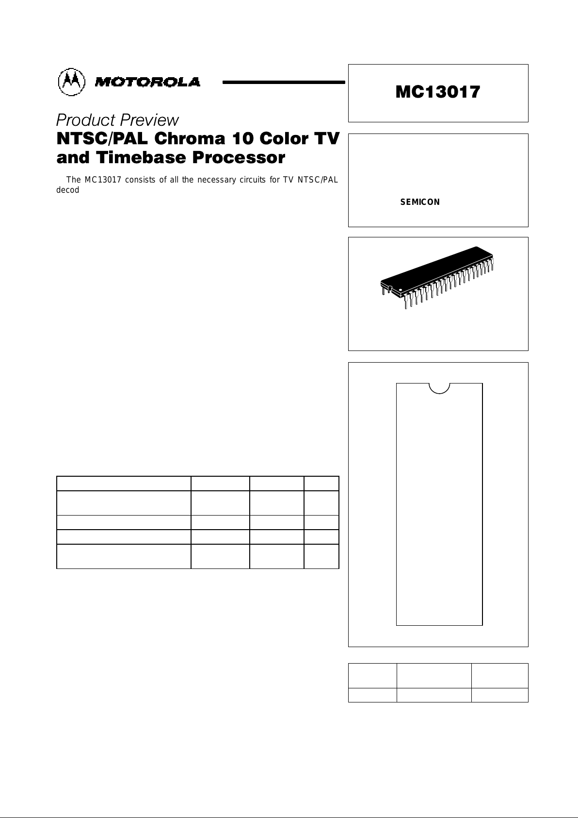
PIN CONNECTIONS
Order this document by MC13017/D
P SUFFIX
PLASTIC PACKAGE
CASE 711
40
1
20
19
212290° FLT
VCO FLT
U I/P
V I/P
18
17
16
15
14
23
24
25
26
27
Xtal Drive
Xtal FB
Gnd
DC Ref & BL
B O/P
ID
Sat
DL C
DL E
ACC
G O/P
R O/P
Sandcastle
Pulse
Brightness
Contrast
X–Ray
H. Freq
PD1
H. Flyback
PD2
H. O/P
H. Gnd
V
CC2
28
29
30
31
32
33
34
35
36
37
38
39
40
13
12
11
10
9
8
7
6
5
4
3
2
1
Chroma I/P
Hue
V
CC1
+ 12 V
Luma I/P
Sync I/P
Sync Sep Cap
V. Height
Ramp Cap
Buffer Ramp
V. Out
V. Feedback
V. Gnd
V
CC3
(Top View)
1
MOTOROLA ANALOG IC DEVICE DATA
The MC13017 consists of all the necessary circuits for TV NTSC/PAL
decoding and timebase processing. It forms a kit set with the MC44301 VIF
and the TDA3190 Sound IF and Power for a low cost, high performance CTV
system.
• On–Chip Sync Separator
• Dual Loop Horizontal Timebase
• Direct Locked Vertical Counter
• X–Ray Protection
• Noise Blanking on Sync Separator
• NTSC/PAL Color Decoding
• Direct Interface with SECAM TDA3030B
• 4.43/3.579 MHz Crystal Reference
• Three DC High Impedance Control Outputs for Contrast, Brightness, and
Saturation
• 12 V Supply
• Vertical Ramp Buffer Output
• Sandcastle Output
• Hue Control
MAXIMUM RATINGS
(TA = 25°C, unless otherwise noted.)
Rating
Symbol Value Unit
Power Supply Voltages V
CC1
, V
CC3
V
CC2
15
10
V
Operating Temperature Range T
A
0 to +70 5C
Storage Temperature Range T
stg
– 55 to +125 °C
Horizontal Output Voltage
Vertical Output Voltage
V
OH
V
OV
8.0
4.0
V
Motorola, Inc. 1995This document contains information on a product under development. Motorola reserves the right
to change or discontinue this product without notice.
Page 2
MC13017
2
MOTOROLA ANALOG IC DEVICE DATA
PIN FUNCTION DESCRIPTION
Pin Function Description
1 V
CC3
+12 V supply for V
CC2
power regulator.
2 Vert Gnd Vertical output analog ground.
3 Vert Feedback The Ramp on Pin 6 is internally inverted, level shifted and subtracted from the input to Pin 3. The
result appears as an output on an open collector at Pin 4.
4 Vert Out Vertical ramp output to external vertical power drive.
5 Buffer Ramp The vertical buffer ramp output of Pin 6.
6 Ramp Cap The external cap is charged by a current controlled through vertical height control Pin 7 to
produce a vertical ramp. The discharge of the cap is controlled internally by the vertical counter.
7 Vert Height Current input for vertical height control.
8, 9 Sync Sep Cap,
Sync I/P
Sync separator input is a NPN transistor stage with the signal presented at its base with a peak
level of about 4.0 V. The emitter is brought out to Pin 8 through a 200 Ω resistor so that a
capacitor with a series resistor may be connected. The circuit behaves as a peak detector with a
slicing level controlled by the choice of charge and discharge resistors. An additional time
constant is connected through a diode to prevent the slice level from riding up on the field sync.
11 V
CC1
+12 V supply for chroma.
12 Hue This is Hue control for NTSC system. It should be connected to V
CC1
at PAL system. When
voltage at Pin 12 is smaller than 8.0 V , NTSC mode is selected.
15 DL E Delay line drive open emitter terminal.
16 DL C Delay line drive open collector terminal.
18 ID Filter An external filter cap is connected at this pin for ID circuit.
19, 20 V, U V, U inputs after delay line to detectors.
21 90° Filter 90° phase shifter filter.
22 VCO Filter Color reference VCO filter.
23
24
Xtal 2
Xtal 1
A 4.43 MHz (PAL), or 3.579 MHz (NTSC) crystal is connected to the internal VCO for color
subcarrier reference frequency.
30 Sandcastle
Pulse Output
The Sandcastle Pulse Output is delivered through 200 Ω from an emitter–follower with 10 kΩ
pull–down. The blanking duration is determined by the applied flyback pulse. The burst gate
determined by the second half of the flyback levels are: Blanking (4.0 V), Burst Gate (11 V).
35 PD1 Horizontal phase detector current output. The PLL 1 is locked to the sync input
with 2H oscillator.
36 Horiz Flyback Horizontal flyback, a positive input pulse exceeded threshold of 1.0 V is required, input
impedance is between 600 and 2.0 kΩ so that a minimum of 0.5 mA current
is needed to exceed the threshold voltage. The recommended peak current is
2.0 mA.
37 PD2 Second horizontal phase detector current output. The function of PLL 2 is to adjust the horizontal
drive in order to maintain the flyback in phase with the oscillator.
38 Horiz Out This is a saturated NPN transistor with a 2.0 kΩ internal load to regulate
supply V
CC2.
39 Horiz Gnd Horizontal analog output grounding should be connected nearby the external horizontal output
stage.
40 V
CC2
Regulated supply to horizontal timebase section. A diode is in series with 270 Ω from
V
CC3
+ 12 V to block the high voltage startup supply of 10 mA for horizontal oscillator.
Page 3

MC13017
3
MOTOROLA ANALOG IC DEVICE DATA
P SUFFIX
PLASTIC PACKAGE
CASE 711–03
ISSUE C
OUTLINE DIMENSIONS
NOTES:
1. POSITIONAL TOLERANCE OF LEADS (D), SHALL
BE WITHIN 0.25 (0.010) AT MAXIMUM MATERIAL
CONDITION, IN RELATION TO SEATING PLANE
AND EACH OTHER.
2. DIMENSION L TO CENTER OF LEADS WHEN
FORMED PARALLEL.
3. DIMENSION B DOES NOT INCLUDE MOLD FLASH.
1 20
40 21
B
A
C
SEATING
PLANE
DFGH
K
N
M
J
L
DIM MIN MAX MIN MAX
INCHESMILLIMETERS
A 51.69 52.45 2.035 2.065
B 13.72 14.22 0.540 0.560
C 3.94 5.08 0.155 0.200
D 0.36 0.56 0.014 0.022
F 1.02 1.52 0.040 0.060
G 2.54 BSC 0.100 BSC
H 1.65 2.16 0.065 0.085
J 0.20 0.38 0.008 0.015
K 2.92 3.43 0.115 0.135
L 15.24 BSC 0.600 BSC
M 0 15 0 15
N 0.51 1.02 0.020 0.040
_ _ _ _
Page 4

MC13017
4
MOTOROLA ANALOG IC DEVICE DATA
Motorola reserves the right to make changes without further notice to any products herein. Motorola makes no warranty , representation or guarantee regarding
the suitability of its products for any particular purpose, nor does Motorola assume any liability arising out of the application or use of any product or circuit, and
specifically disclaims any and all liability, including without limitation consequential or incidental damages. “Typical” parameters can and do vary in different
applications. All operating parameters, including “T ypicals” must be validated for each customer application by customer’s technical experts. Motorola does
not convey any license under its patent rights nor the rights of others. Motorola products are not designed, intended, or authorized for use as components in
systems intended for surgical implant into the body, or other applications intended to support or sustain life, or for any other application in which the failure of
the Motorola product could create a situation where personal injury or death may occur. Should Buyer purchase or use Motorola products for any such
unintended or unauthorized application, Buyer shall indemnify and hold Motorola and its officers, employees, subsidiaries, affiliates, and distributors harmless
against all claims, costs, damages, and expenses, and reasonable attorney fees arising out of, directly or indirectly, any claim of personal injury or death
associated with such unintended or unauthorized use, even if such claim alleges that Motorola was negligent regarding the design or manufacture of the part.
Motorola and are registered trademarks of Motorola, Inc. Motorola, Inc. is an Equal Opportunity/Affirmative Action Employer.
How to reach us:
USA /EUROPE: Motorola Literature Distribution; JAPAN: Nippon Motorola Ltd.; Tatsumi–SPD–JLDC, Toshikatsu Otsuki,
P.O. Box 20912; Phoenix, Arizona 85036. 1–800–441–2447 6F Seibu–Butsuryu–Center, 3–14–2 Tatsumi Koto–Ku, Tokyo 135, Japan. 03–3521–8315
MFAX: RMFAX0@email.sps.mot.com – TOUCHTONE (602) 244–6609 HONG KONG: Motorola Semiconductors H.K. Ltd.; 8B Tai Ping Industrial Park,
INTERNET: http://Design–NET.com 51 Ting Kok Road, Tai Po, N.T., Hong Kong. 852–26629298
MC13017/D
*MC13017/D*
◊
 Loading...