

Page 1
SEMICONDUCTOR TECHNICAL DATA
1
REV 1
Motorola, Inc. 1997
2/97
The MC12430 is a general purpose synthesized clock source targeting
applications that require both serial and parallel interfaces. Its internal
VCO will operate over a range of frequencies from 400 to 800MHz. The
differential PECL output can be configured to be the VCO frequency
divided by 1, 2, 4 or 8. With the output configured to divide the VCO
frequency by 2, and with a 16.000MHz external quartz crystal used to
provide the reference frequency, the output frequency can be specified in
1MHz steps. The PLL loop filter is fully integrated so that no external
components are required.
• 50 to 800MHz Differential PECL Outputs
• ±25ps Peak–to–Peak Output Jitter
• Fully Integrated Phase–Locked Loop
• Minimal Frequency Over–Shoot
• Synthesized Architecture
• Serial 3–Wire Interface
• Parallel Interface for Power–Up
• Quartz Crystal Interface
• 28–Lead PLCC Package
• Operates from 3.3V or 5.0V Power Supply
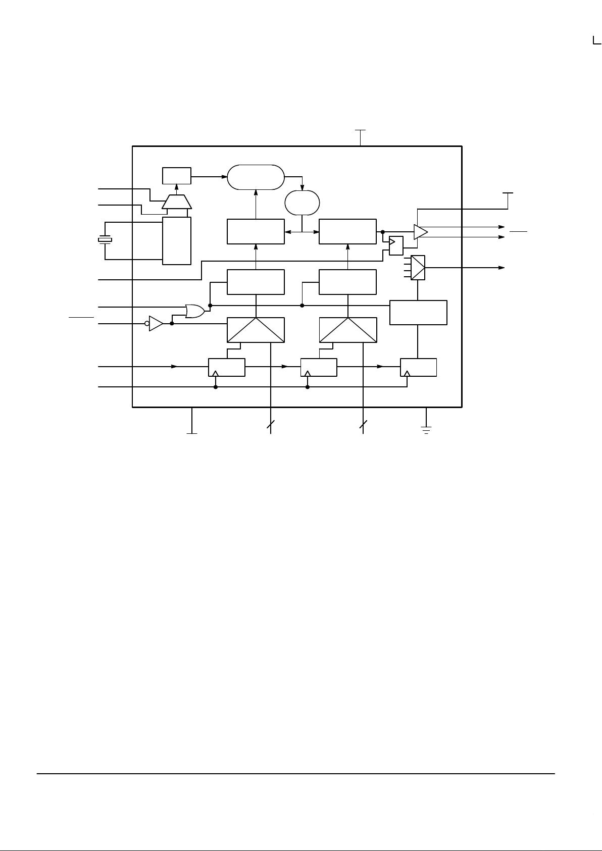
Functional Description
The internal oscillator uses the external quartz crystal as the basis of
its frequency reference. The output of the reference oscillator is divided
by 8 before being sent to the phase detector. With a 16MHz crystal, this
provides a reference frequency of 2MHz. Although this data sheet
illustrates functionality only for a 16MHz crystal, any crystal in the
10–20MHz range can be used.
The VCO within the PLL operates over a range of 400 to 800MHz. Its output is scaled by a divider that is configured by either
the serial or parallel interfaces. The output of this loop divider is applied to the phase detector.
The phase detector and loop filter attempt to force the VCO output frequency to be M times the reference frequency by
adjusting the VCO control voltage. Note that for some values of M (either too high or too low) the PLL will not achieve loop lock.
The output of the VCO is also passed through an output divider before being sent to the PECL output driver. This output divider
(N divider) is configured through either the serial or the parallel interfaces, and can provide one of four division ratios (1, 2, 4 or 8).
This divider extends performance of the part while providing a 50% duty cycle.
The output driver is driven differentially from the output divider, and is capable of driving a pair of transmission lines terminated
in 50Ω to VCC – 2.0. The positive reference for the output driver and the internal logic is separated from the power supply for the
phase–locked loop to minimize noise induced jitter.
The configuration logic has two sections: serial and parallel. The parallel interface uses the values at the M[8:0] and N[1:0]
inputs to configure the internal counters. Normally, on system reset, the P_LOAD
input is held LOW until sometime after power
becomes valid. On the LOW–to–HIGH transition of P_LOAD
, the parallel inputs are captured. The parallel interface has priority
over the serial interface. Internal pullup resistors are provided on the M[8:0] and N[1:0] inputs to reduce component count in the
application of the chip.
The serial interface centers on a fourteen bit shift register. The shift register shifts once per rising edge of the S_CLOCK input.
The serial input S_DATA must meet setup and hold timing as specified in the AC Characteristics section of this document. The
configuration latches will capture the value of the shift register on the HIGH–to–LOW edge of the S_LOAD input. See the
programming section for more information.
The TEST output reflects various internal node values, and is controlled by the T[2:0] bits in the serial data stream. See the
programming section for more information.
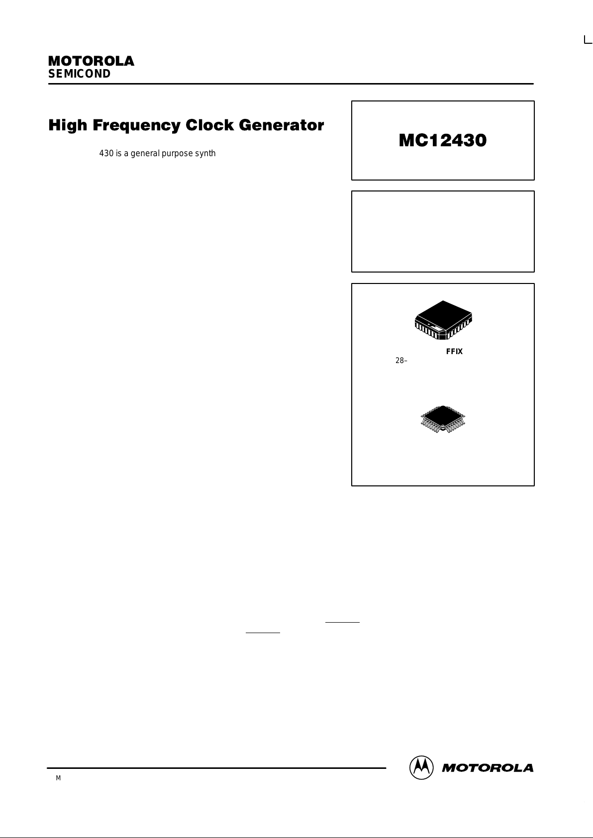
HIGH FREQUENCY PLL
CLOCK GENERATOR
FN SUFFIX
28–LEAD PLCC PACKAGE
CASE 776–02
FA SUFFIX
32–LEAD TQFP PACKAGE
CASE 873A–02
Page 2
MC12430
MOTOROLA TIMING SOLUTIONS
BR1333 — Rev 6
2
1
N[1]
N[0]
M[8]
M[7]
M[6]
M[5]
M[4]XTAL1
XTAL_SEL
FREF_EXT
PLL–V
CC
S_LOAD
S_DATA
S_CLOCK
4
3
2
28
27
26
25
24
23
22
21
20
19
18
17
16
15
14
13
12
11109
7
8
6
5
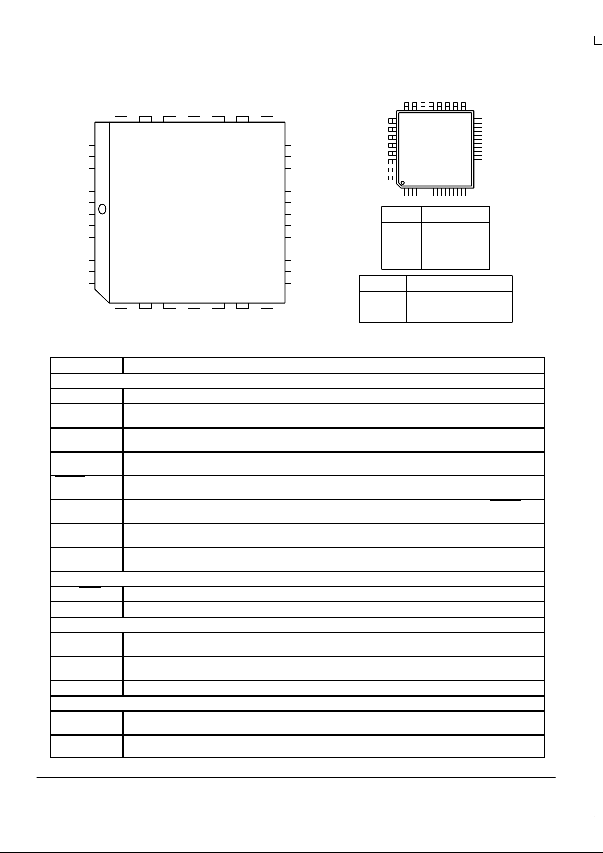
28–Lead Pinout (Top View)
P_LOAD
VCCFOUT FOUT GND VCCTEST GND
M[3]M[2]M[1]M[0]
OE
XTAL2
N[1:0]
0 0
0 1
1 0
1 1
Output Division
2
4
8
1
Input
XTAL_SEL
OE
0
FREF_EXT
Disabled
1
XTAL
Enabled
32–Lead Pinout
TBD
PIN DESCRIPTIONS
Pin Name Function
Inputs
XTAL1, XTAL2 These pins form an oscillator when connected to an external series–resonant crystal.
S_LOAD
(Int. Pulldown)
This pin loads the configuration latches with the contents of the shift registers. The latches will be transparent when this
signal is HIGH, thus the data must be stable on the HIGH–to–LOW transition of S_LOAD for proper operation.
S_DATA
(Int. Pulldown)
This pin acts as the data input to the serial configuration shift registers.
S_CLOCK
(Int. Pulldown)
This pin serves to clock the serial configuration shift registers. Data from S_DATA is sampled on the rising edge.
P_LOAD
(Int. Pullup)
This pin loads the configuration latches with the contents of the parallel inputs .The latches will be transparent when this
signal is LOW, thus the parallel data must be stable on the LOW–to–HIGH transition of P_LOAD
for proper operation.
M[8:0]
(Int. Pullup)
These pins are used to configure the PLL loop divider. They are sampled on the LOW–to–HIGH transition of P_LOAD. M[8]
is the MSB, M[0] is the LSB.
N[1:0]
(Int. Pullup)
These pins are used to configure the output divider modulus. They are sampled on the LOW–to–HIGH transition of
P_LOAD
.
OE
(Int. Pullup)
Active HIGH Output Enable. The Enable is synchronous to eliminate possibility of runt pulse generation on the F
OUT
output.
Outputs
F
OUT
, F
OUT
These differential positive–referenced ECL signals (PECL) are the output of the synthesizer.
TEST The function of this output is determined by the serial configuration bits T[2:0]. The output is single–ended ECL.
Power
V
CC
This is the positive supply for the internal logic and the output buffer of the chip, and is connected to +3.3V or 5.0V
(VCC = PLL_VCC). Current drain through VCC ≈ 85mA.
PLL_V
CC
This is the positive supply for the PLL, and should be as noise–free as possible for low–jitter operation. This supply is
connected to +3.3V or 5.0V (VCC = PLL_VCC). Current drain through PLL_VCC ≈ 15mA.
GND These pins are the negative supply for the chip and are normally all connected to ground.
Other
FREF_EXT
(Int. Pulldown)
LVCMOS/CMOS input which can be used as the PLL reference.
XTAL_SEL
(Int. Pullup)
LVCMOS/CMOS input that selects between the crystal and the FREF_EXT source for the PLL reference signal. A HIGH
selects the crystal input.
Page 3
MC12430
TIMING SOLUTIONS
BR1333 — Rev 6
3 MOTOROLA
9–BIT SR 2–BIT SR 3–BIT SR
DIV 8
MC12430 BLOCK DIAGRAM
16MHz
S_LOAD
P_LOAD
S_DATA
S_CLOCK
XTAL1
XTAL2
OSC
4
5
PHASE
DETECTOR
28
7
9–BIT DIV M
COUNTER
LATCH
VCO
DIV N
(1, 2, 4, 8)
LATCH
400–800
MHz
FOUT
FOUT
+3.3 or 5.0V
25
24
23
V
CC0
LATCH
TEST
20
+3.3 or 5.0V
PLL_V
CC
2MHz
F
REF
01
27
26
01
V
CC1
+3.3 or 5.0V
M[8:0]
9
8:16
N[1:0]
2
17, 1821 22, 19
OE
6
FREF_EXT
2
XTAL_SEL
3
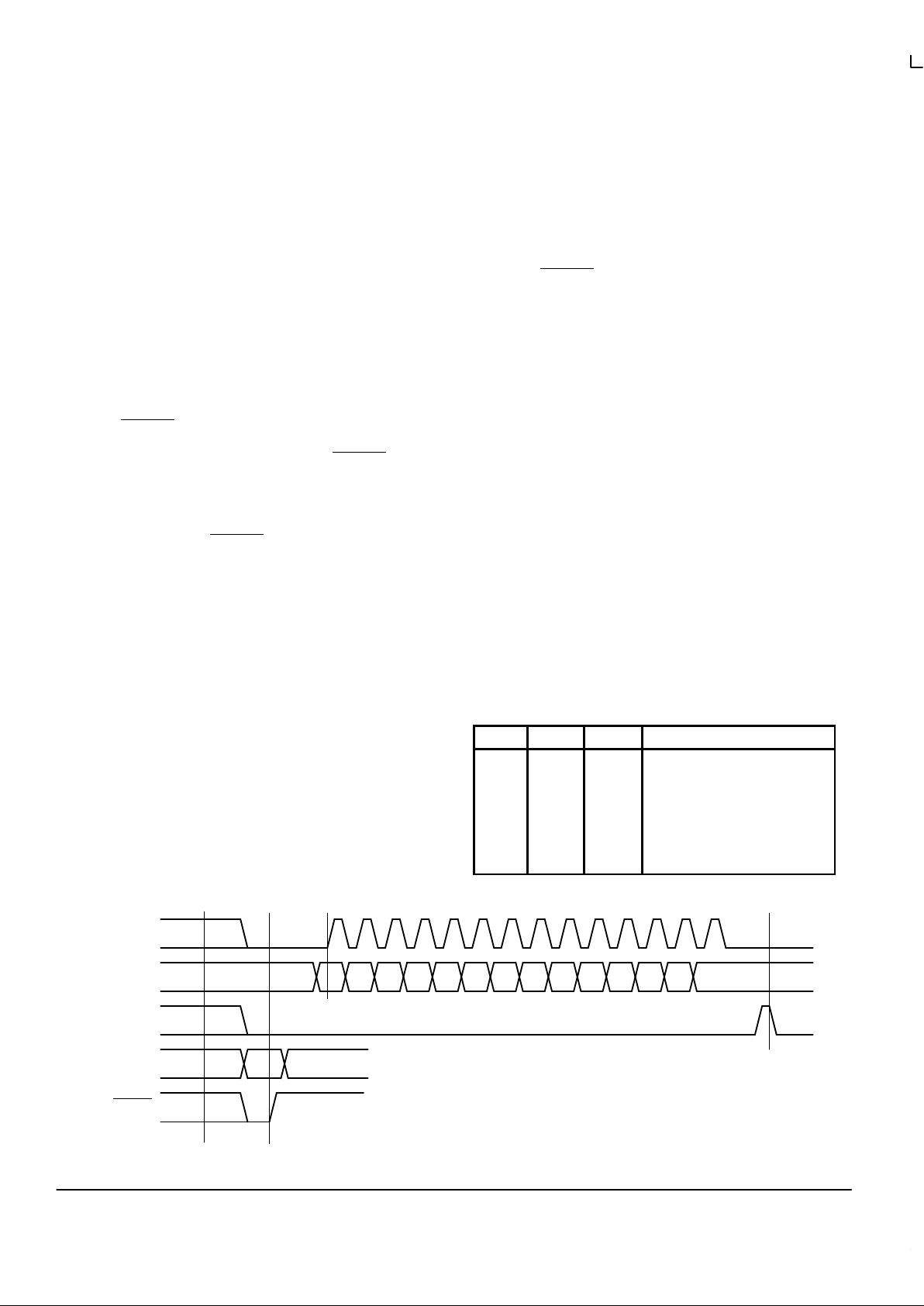
PROGRAMMING INTERF ACE
Programming the device amounts to properly configuring
the internal dividers to produce the desired frequency at the
outputs. The output frequency can by represented by this
formula:
FOUT = (F
XTAL
÷ 8) x M ÷ N (1)
Where F
XTAL
is the crystal frequency, M is the loop divider
modulus, and N is the output divider modulus. Note that it is
possible to select values of M such that the PLL is unable to
achieve loop lock. To avoid this, always make sure that M is
selected to be 200 ≤ M ≤ 400 for any input reference.
Assuming that a 16MHz reference frequency is used the
above equation reduces to:
FOUT = 2 x M ÷ N
Substituting the four values for N (1, 2, 4, 8) yields:
FOUT = 2M, FOUT = M,
FOUT = M ÷ 2 and FOUT = M ÷ 4
for 200 < M < 400
The user can identify the proper M and N values for the
desired frequency from the above equations. The four output
frequency ranges established by N are 400–800MHz,
200–400MHz, 100–200MHz and 50–100MHz respectively.
From these ranges the user will establish the value of N
required, then the value of M can be calculated based on the
appropriate equation above. For example if an output
frequency of 131MHz was desired the following steps would
be taken to identify the appropriate M and N values. 131MHz
falls within the frequency range set by an N value of 4 so N
[1:0] = 01. For N = 4 FOUT = M ÷ 2 and M = 2 x FOUT.
Therefore M = 131 x 2 = 262, so M[8:0] = 100000110.
Following this same procedure a user can generate any
whole frequency desired between 50 and 800MHz. Note that
for N > 2 fractional values of FOUT can be realized. The size
of the programmable frequency steps (and thus the indicator
of the fractional output frequencies acheivable) will be equal
to FXTAL ÷ 8 ÷ N.
For input reference frequencies other than 16MHz the set
of appropriate equations can be deduced from equation 1.
For computer applications another useful frequency base
would be 16.666MHz. From this reference one can generate
a family of output frequencies at multiples of the 33.333MHz
PCI clock. As an example to generate a 133.333MHz clock
Page 4
MC12430
MOTOROLA TIMING SOLUTIONS
BR1333 — Rev 6
4
from a 16.666MHz reference the following M and N values
would be used:
FOUT = 16.666 ÷ 8 x M ÷ N = 2.083333 x M ÷ N
Let N = 4, M = 133.3333 ÷ 2.083333 x 4 = 256
The value for M falls within the constraints set for PLL
stability, therefore N[1:0] = 01 and M[8:0} = 10000000. If the
value for M fell outside of the valid range a different N value
would be selected to try to move M in the appropriate
direction.
The M and N counters can be loaded either through a
parallel or serial interface. The parallel interface is controlled
via the P_LOAD
signal such that a LOW to HIGH transition
will latch the information present on the M[8:0] and N[1:0]
inputs into the M and N counters. When the P_LOAD
signal is
LOW the input latches will be transparent and any changes
on the M[8:0] and N[1:0] inputs will affect the FOUT output
pair. To use the serial port the S_CLOCK signal samples the
information on the S_DA TA line and loads it into a 14 bit shift
register. Note that the P_LOAD
signal must be HIGH for the
serial load operation to function. The Test register is loaded
with the first three bits, the N register with the next two and
the M register with the final eight bits of the data streeam on
the S_DATA input. For each register the most significant bit is
loaded first (T2, N1 and M8). A pulse on the S_LOAD pin
after the shift register is fully loaded will transfer the divide
values into the counters. The HIGH to LOW transition on the
S_LOAD input will latch the new divide values into the
counters. NO TAG illustrates the timing diagram for both a
parallel and a serial load of the MC12430 synthesizer.
M[8:0] and N[1:0] are normally specified once at power–up
through the parallel interface, and then possibly again
through the serial interface. This approach allows the
application to come up at one frequency and then change or
fine–tune the clock as the ability to control the serial interface
becomes available. To minimize transients in the frequency
domain, the output should be varied in the smallest step size
possible. The bandwidth of the PLL is such that frequency
stepping in 1MHz steps at the maximum S_CLOCK
frequency or less will cause smooth, controlled slewing of the
output frequency.
The TEST output provides visibility for one of the several
internal nodes as determined by the T[2:0] bits in the serial
configuration stream. It is not configurable through the
parallel interface. The T2, T1 and T0 control bits are preset to
‘000’ when P_LOAD
is LOW so that the PECL FOUT outputs
are as jitter–free as possible. Any active signal on the TEST
output pin will have detrimental affects on the jitter of the
PECL output pair. In normal operations, jitter specifications
are only guaranteed if the TEST output is static. The serial
configuration port can be used to select one of the alternate
functions for this pin.
Most of the signals available on the TEST output pin are
useful only for performance verification of the MC12430
itself. However the PLL bypass mode may be of interest at
the board level for functional debug. When T[2:0] is set to 110
the MC12430 is placed in PLL bypass mode. In this mode the
S_CLOCK input is fed directly into the M and N dividers. The
N divider drives the FOUT differential pair and the M counter
drives the TEST output pin. In this mode the S_CLOCK input
could be used for low speed board level functional test or
debug. Bypassing the PLL and driving FOUT directly gives
the user more control on the test clocks sent through the
clock tree. NO TAG shows the functional setup of the PLL
bypass mode. Because the S_CLOCK is a CMOS level the
input frequency is limited to 250MHz or less. This means the
fastest the FOUT pin can be toggled via the S_CLOCK is
250MHz as the minimum divide ratio of the N counter is 1.
Note that the M counter output on the TEST output will not be
a 50% duty cycle due to the way the divider is implemented.
T2 T1 T0 TEST (Pin 20)
0
0
0
0
1
1
1
1
0
0
1
1
0
0
1
1
0
1
0
1
0
1
0
1
SHIFT REGISTER OUT
HIGH
FREF
M COUNTER OUT
FOUT
LOW
PLL BYPASS
FOUT/4
Figure 1. Timing Diagram
S_CLOCK
S_DATA
S_LOAD
M[8:0]
N[1:0]
P_LOAD
T2 T1 T0 N1 N0 M8 M7 M6 M5 M4 M3 M2 M1
M0
M, N
First
Bit
Last
Bit
Page 5

MC12430
TIMING SOLUTIONS
BR1333 — Rev 6
5 MOTOROLA
Figure 2. Serial Test Clock Block Diagram
FDIV4
MCNT
LOW
FOUT
MCNT
FREF
HIGH
TEST
MUX
7
0
TEST
FOUT
(VIA ENABLE GATE)
N DIVIDE
(1, 2, 4, 8)
0
1
PLL 12430
LATCH
Reset
PLOADB
M COUNTER
SLOAD
T0
T1
T2
VCO_CLK
SHIFT
REG
14–BIT
DECODE
SDATA
SCLOCK
MCNT
FREF
SEL_CLK
•
T2=T1=1, T0=0: Test Mode
•
SCLOCK is selected, MCNT is on TEST output, SCLOCK DIVIDE BY N is on FOUT pin
PLOADB acts as reset for test pin latch. When latch reset T2 data is shifted out TEST pin.
DC CHARACTERISTICS (TA = 0° to 70°C, VCC = 3.3V to 5.0V ±5%)
Symbol Characteristic Min Typ Max Unit Condition
V
IH
Input HIGH Voltage 2.0 V VCC = 3.3 to 5.0V
V
IL
Input LOW Voltage 0.8 V VCC = 3.3 to 5.0V
I
IN
Input Current 1.0 mA
V
OH
Output HIGH Voltage 2.17 2.50 V V
CC0
= 3.3V
1
V
OL
Output LOW Voltage 1.41 1.76 V V
CC0
= 3.3V
1
I
CC
Power Supply Current V
CC
PLL_V
CC
85
15
100
20
mA
1. Output levels will vary 1:1 with V
CC0
variation.
Page 6

MC12430
MOTOROLA TIMING SOLUTIONS
BR1333 — Rev 6
6
AC CHARACTERISTICS (TA = 0° to 70°C, VCC = 3.3V to 5.0V ±5%)
Symbol Characteristic Min Max Unit Condition
F
MAXI
Maximum Input Frequency S_CLOCK
Xtal Oscillator
FREF_EXT
10
10
10
20
Note 3.
MHz Note 2.
F
MAXO
Maximum Output Frequency VCO (Internal)
FOUT
400
50
800
800
MHz
t
LOCK
Maximum PLL Lock Time 10 ms
t
jitter
Cycle–to–Cycle Jitter (Peak–to–Peak) Note 4. ±25
±65
ps N = 2, 4, 8; Note 5.
N = 1; Note 5.
t
s
Setup Time S_DATA to S_CLOCK
S_CLOCK to S_LOAD
M, N to P_LOAD
20
20
20
ns
t
h
Hold Time S_DATA to S_CLOCK
M, N to P_LOAD
20
20
ns
tpw
MIN
Minimum Pulse Width S_LOAD
P_LOAD
50
50
ns
tr, t
f
Output Rise/Fall FOUT 300 800 ps 20%–80%
2. 10MHz is the maximum frequency to load the feedback devide registers. S_CLOCK can be switched at higher frequencies when used as a
test clock in TEST_MODE 6.
3. Maximum frequency on FREF_EXT is a function of the internal M counter limitations. The phase detector can handle up to 100MHz on the input,
but the M counter must remain in the valid range of 200 ≤ M ≤ 400. See the programming section on page 3 of this data sheet fore more details.
4. See Applications Information below for additional information.
5. 50Ω to VCC – 2.0V pull–down.
APPLICATIONS INFORMATION
Using the On–Board Crystal Oscillator
The MC12430 features a fully integrated on–board crystal
oscillator to minimize system implementation costs. The
oscillator is a series resonant, multivibrator type design as
opposed to the more common parallel resonant oscillator
design. The series resonant design provides better stability
and eliminates the need for large on chip capacitors. The
oscillator is totally self contained so that the only external
component required is the crystal. As the oscillator is
somewhat sensitive to loading on its inputs the user is
advised to mount the crystal as close to the MC12430 as
possible to avoid any board level parasitics. To facilitate
co–location surface mount crystals are recommended, but
not required.
The oscillator circuit is a series resonant circuit and thus
for optimum performance a series resonant crystal should be
used. Unfortunately most crystals are characterized in a
parallel resonant mode. Fortunately there is no physical
difference between a series resonant and a parallel resonant
crystal. The difference is purely in the way the devices are
characterized. As a result a parallel resonant crystal can be
used with the MC12430 with only a minor error in the desired
frequency. A parallel resonant mode crystal used in a series
resonant circuit will exhibit a frequency of oscillation a few
hundred ppm lower than specified, a few hundred ppm
translates to kHz inaccuracies. In a general computer
application this level of inaccuracy is immaterial. Table 1
below specifies the performance requirements of the crystals
to be used with the MC12430.
Table 1. Crystal Specifications
Parameter Value
Crystal Cut Fundamental AT Cut
Resonance Series Resonance*
Frequency Tolerance ±75ppm at 25°C
Frequency/Temperature Stability ±150pm 0 to 70°C
Operating Range 0 to 70°C
Shunt Capacitance 5–7pF
Equivalent Series Resistance (ESR) 50 to 80Ω
Correlation Drive Level 100µW
Aging 5ppm/Yr (First 3 Y ears)
* See accompanying text for series versus parallel resonant
discussion.
Page 7

MC12430
TIMING SOLUTIONS
BR1333 — Rev 6
7 MOTOROLA
Power Supply Filtering
The MC12430 is a mixed analog/digital product and as
such it exhibits some sensitivities that would not necessarily
be seen on a fully digital product. Analog circuitry is naturally
susceptible to random noise, especially if this noise is seen
on the power supply pins. The MC12430 provides separate
power supplies for the digital ciruitry (VCC) and the internal
PLL (PLL_VCC) of the device. The purpose of this design
technique is to try and isolate the high switching noise digital
outputs from the relatively sensitive internal analog
phase–locked loop. In a controlled environment such as an
evaluation board this level of isolation is sufficient. However,
in a digital system environment where it is more difficult to
minimize noise on the power supplies a second level of
isolation may be required. The simplest form of isolation is a
power supply filter on the PLL_VCC pin for the MC12430.
NO TAG illustrates a typical power supply filter scheme.
The MC12430 is most susceptible to noise with spectral
content in the 1KHz to 1MHz range. Therefore the filter
should be designed to target this range. The key parameter
that needs to be met in the final filter design is the DC voltage
drop that will be seen between the VCC supply and the
PLL_VCC pin of the MC12430. From the data sheet the
I
PLL_VCC
current (the current sourced through the PLL_VCC
pin) is typically 15mA (20mA maximum), assuming that a
minimum of 3.0V must be maintained on the PLL_VCC pin
very little DC voltage drop can be tolerated when a 3.3V V
CC
supply is used. The resistor shown in NO TAG must have a
resistance of 10–15Ω to meet the voltage drop criteria. The
RC filter pictured will provide a broadband filter with
approximately 100:1 attenuation for noise whose spectral
content is above 20KHz. As the noise frequency crosses the
series resonant point of an individual capacitor it’s overall
impedance begins to look inductive and thus increases with
increasing frequency. The parallel capacitor combination
shown ensures that a low impedance path to ground exists
for frequencies well above the bandwidth of the PLL.
Figure 3. Power Supply Filter
PLL_VCC
VCC
MC12430
0.01µF
22
µ
F
0.01
µ
F
3.3V or
5.0V
RS=10–15
Ω
A higher level of attenuation can be acheived by replacing
the resistor with an appropriate valued inductor. A 1000µH
choke will show a significant impedance at 10KHz
frequencies and above. Because of the current draw and the
voltage that must be maintained on the PLL_VCC pin a low
DC resistance inductor is required (less than 15Ω). Generally
the resistor/capacitor filter will be cheaper, easier to
implement and provide an adequate level of supply filtering.
The MC12430 provides sub–nanosecond output edge
rates and thus a good power supply bypassing scheme is a
must. NO TAG shows a representaive board layout for the
MC12430. There exists many different potential board
layouts and the one pictured is but one. The important aspect
of the layout in NO TAG is the low impedance connections
between VCC and GND for the bypass capacitors.
Combining good quality general purpose chip capacitors with
good PCB layout techniques will produce effective capacitor
resonances at frequencies adequate to supply the
instantaneous switching current for the 12430 outputs. It is
imperative that low inductance chip capacitors are used; it is
equally important that the board layout does not introduce
back all of the inductance saved by using the leadless
capacitors. Thin interconnect traces between the capacitor
and the power plane should be avoided and multiple large
vias should be used to tie the capacitors to the buried power
planes. Fat interconnect and large vias will help to minimize
layout induced inductance and thus maximize the series
resonant point of the bypass capacitors.
Figure 4. PCB Board Layout for MC12430
C2
1
C3
R1
Xtal
C1 C1
R1 = 10–15
Ω
C1 = 0.01µF
C2 = 22
µ
F
C3 = 0.1
µ
F
= V
CC
= GND
= Via
Note the dotted lines circling the crystal oscillator
connection to the device. The oscillator is a series resonant
circuit and the voltage amplitude across the crystal is
relatively small. It is imperative that no actively switching
signals cross under the crystal as crosstalk energy coupled
to these lines could significantly impact the jitter of the device.
Special attention should be paid to the layout of the crystal to
ensure a stable, jitter free interface between the crystal and
the on–board oscillator.
Although the MC12430 has several design features to
minimize the susceptibility to power supply noise (isolated
power and grounds and fully differential PLL) there still may
be applications in which overall performance is being
degraded due to system power supply noise. The power
supply filter and bypass schemes discussed in this section
Page 8

MC12430
MOTOROLA TIMING SOLUTIONS
BR1333 — Rev 6
8
should be adequate to eliminate power supply noise related
problems in most designs.
Jitter Performance of the MC12430
The MC12430 exhibits long term and cycle–to–cycle jitter
which rivals that of SAW based oscillators. This jitter
performance comes with the added flexibility one gets with a
synthesizer over a fixed frequency oscillator.
Figure 5. RMS PLL Jitter versus VCO Frequency
0
5
10
15
20
25
400 500 600 700 800
N=2
N=4
N=8
VCO Frequency (MHz)
RMS Jitter (ps)
Figure 5 illustrates the RMS jitter performance of the
MC12430 across its specified VCO frequency range. Note
that the jitter is a function of both the output frequency as well
as the VCO frequency, however the VCO frequency shows a
much stronger dependence. The data presented has not
been compensated for trigger jitter, this fact provides a
measure of guardband to the reported data. In addition the
data represents long term period jitter, the cycle–to–cycle
jitter could not be measured to the level of accuracy required
with available test equipment but certainly will be smaller
than the long term period jitter.
The most commonly specified jitter parameter is
cycle–to–cycle jitter. Unfortunately with today’s high
performance measurement equipment there is no way to
measure this parameter for jitter performance in the class
demonstrated by the MC12430. As a result different methods
are used which approximate cycle–to–cycle jitter. The typical
method of measuring the jitter is to accumulate a large
number of cycles, create a histogram of the edge placements
and record peak–to–peak as well as standard deviations of
the jitter. Care must be taken that the measured edge is the
edge immediately following the trigger edge. The
oscilloscope cannot collect adjacent pulses, rather it collects
pulses from a very large sample of pulses. It is safe to
assume that collecting pulse information in this mode will
produce period jitter values somewhat larger than if
consecutive cycles (cycle–to–cycle jitter) were measured. All
of the jitter data reported on the MC12430 was collected in
this manner.
Figure 6. RMS Jitter versus Output Frequency
0
5
10
15
20
25
25 50 75 100 125 150 175 200 225 250 275 300 325 350 375 400
Output Frequency (MHz)
RMS Jitter (ps)
6.25ps Reference
Figure 6 shows the jitter as a function of the output
frequency. For the 12430 this information is probably of more
importance. The flat line represents an RMS jitter value that
corresponds to an 8 sigma ±25ps peak–to–peak long term
period jitter. The graph shows that for output frequencies
from 87.5 to 400MHz the jitter falls within the ±25ps
peak–to–peak specification. The general trend is that as the
output frequency is decreased the output edge jitter will
increase.
The jitter data from Figure 5 and Figure 6 do not include
the performance of the 12430 when the output is in the divide
by 1 mode. In divide by one mode the output signal is a
digitally doubled version of the VCO output. The period of the
outputs of the digital doubler is dependent on the duty cycle
of the VCO output. Since the VCO output duty cycle cannot
be guaranteed to be always 50% the resulting 12430 output
in divide by one mode will be bimodal at times. Since a
bimodal distribution cannot be acurately represented with an
rms value, peak–to–peak values of jitter for the divide by one
mode are presented.
NO TAG shows the peak–to–peak jitter of the 12430
output in divide by one mode as a function of output
frequency. Notice that as with the other modes the jitter
improves with increasing frequency. The ± 65ps shown in the
data sheet table represents a conservative value of jitter,
especially for the higher vco, and thus output frequencies.
Figure 7. Peak–to–Peak Jitter versus
Output Frequency
40
60
80
100
120
140
400 500 600 700 800
Spec Limit
N=1
Output Frequency (MHz)
Peak–to–Peak Jitter (ps)
The jitter data presented should provide users with
enough information to determine the effect on their overall
Page 9

MC12430
TIMING SOLUTIONS
BR1333 — Rev 6
9 MOTOROLA
timing budget. The jitter performance meets the needs of
most system designs while adding the flexibility of frequency
margining and field upgrades. These features are not
available with a fixed frequency SAW oscillator.
Output Voltage Swing vs Frequency
In the divide by one mode the output rise and fall times will
limit the peak to peak output voltage swing. For a 400MHz
output the peak to peak swing of the 12430 output will be
approximately 700mV. This swing will gradually degrade as
the output frequency increases, at 800MHz the output swing
will be reduced to approximately 400mV. For a worst case
analysis it would be safe to assume that the 12430 output will
always generate at least a 400mV output swing. Note that
most high speed ECL receivers require only a few hundred
millivolt input swings for reliable operation. As a result the
output generated by the 12430 will, under all conditions, be
sufficient for clocking standard ECL devices. Note that if a
larger swing is desired the 12430 could drive a single gate
ECLinPS Lite amplifier like the MC100LVEL16. The LVEL16
will speed up the output edge rates and produce a full swing
ECL output at 800MHz.
Page 10

MC12430
MOTOROLA TIMING SOLUTIONS
BR1333 — Rev 6
10
OUTLINE DIMENSIONS
FN SUFFIX
PLASTIC PLCC PACKAGE
CASE 776–02
ISSUE D
0.007 (0.180) T L
–M
SNSM
0.007 (0.180) T L
–M
SNSM
0.007 (0.180) T L
–M
SNSM
0.010 (0.250) T L
–M
SNSS
0.007 (0.180) T L
–M
SNSM
0.010 (0.250) T L
–M
SNSS
0.007 (0.180) T L
–M
SNSM
0.007 (0.180) T L
–M
SNSM
0.004 (0.100)
SEATING
PLANE
–T
–
12.32
12.32
4.20
2.29
0.33
0.66
0.51
0.64
11.43
11.43
1.07
1.07
1.07
—
2
°
10.42
1.02
12.57
12.57
4.57
2.79
0.48
0.81
—
—
11.58
11.58
1.21
1.21
1.42
0.50
10
°
10.92
—
1.27 BSC
A
B
C
E
F
G
H
J
K
R
U
V
W
X
Y
Z
G1
K1
MIN MINMAX MAX
INCHES MILLIMETERS
DIM
NOTES:
1. DATUMS –L–, –M–, AND –N– DETERMINED
WHERE TOP OF LEAD SHOULDER EXITS
PLASTIC BODY AT MOLD PARTING LINE.
2. DIM G1, TRUE POSITION TO BE MEASURED
AT DATUM –T–, SEATING PLANE.
3. DIM R AND U DO NOT INCLUDE MOLD FLASH.
ALLOWABLE MOLD FLASH IS 0.010 (0.250)
PER SIDE.
4. DIMENSIONING AND TOLERANCING PER ANSI
Y14.5M, 1982.
5. CONTROLLING DIMENSION: INCH.
6. THE PACKAGE TOP MAY BE SMALLER THAN
THE PACKAGE BOTTOM BY UP TO 0.012
(0.300). DIMENSIONS R AND U ARE
DETERMINED AT THE OUTERMOST
EXTREMES OF THE PLASTIC BODY
EXCLUSIVE OF MOLD FLASH, TIE BAR
BURRS, GATE BURRS AND INTERLEAD
FLASH, BUT INCLUDING ANY MISMATCH
BETWEEN THE TOP AND BOTTOM OF THE
PLASTIC BODY.
7. DIMENSION H DOES NOT INCLUDE DAMBAR
PROTRUSION OR INTRUSION. THE DAMBAR
PROTRUSION(S) SHALL NOT CAUSE THE H
DIMENSION TO BE GREATER THAN 0.037
(0.940). THE DAMBAR INTRUSION(S) SHALL
NOT CAUSE THE H DIMENSION TO BE
SMALLER THAN 0.025 (0.635).
VIEW S
B
U
Z
G1
X
VIEW D–D
H
K
F
VIEW S
G
C
Z
A
R
E
J
0.485
0.485
0.165
0.090
0.013
0.026
0.020
0.025
0.450
0.450
0.042
0.042
0.042
—
2
°
0.410
0.040
0.495
0.495
0.180
0.110
0.019
0.032
—
—
0.456
0.456
0.048
0.048
0.056
0.020
10
°
0.430
—
0.050 BSC
–N
–
Y BRK
D
D
W
–M
–
–L
–
28 1
V
G1
K1
Page 11

MC12430
TIMING SOLUTIONS
BR1333 — Rev 6
11 MOTOROLA
OUTLINE DIMENSIONS
FA SUFFIX
TQFP PACKAGE
CASE 873A–02
ISSUE A
DETAIL Y
A
S1
VB
1
8
9
17
25
32
AE
AE
P
DETAIL Y
BASE
N
J
DF
METAL
SECTION AE–AE
G
SEATING
PLANE
R
Q
_
W
K
X
0.250 (0.010)
GAUGE PLANE
E
C
H
DETAIL AD
NOTES:
1. DIMENSIONING AND TOLERANCING PER ANSI
Y14.5M, 1982.
2. CONTROLLING DIMENSION: MILLIMETER.
3. DATUM PLANE –AB– IS LOCATED AT BOTTOM OF
LEAD AND IS COINCIDENT WITH THE LEAD
WHERE THE LEAD EXITS THE PLASTIC BODY AT
THE BOTTOM OF THE PARTING LINE.
4. DATUMS –T–, –U–, AND –Z– TO BE DETERMINED
AT DATUM PLANE –AB–.
5. DIMENSIONS S AND V TO BE DETERMINED AT
SEATING PLANE –AC–.
6. DIMENSIONS A AND B DO NOT INCLUDE MOLD
PROTRUSION. ALLOWABLE PROTRUSION IS
0.250 (0.010) PER SIDE. DIMENSIONS A AND B
DO INCLUDE MOLD MISMATCH AND ARE
DETERMINED AT DATUM PLANE –AB–.
7. DIMENSION D DOES NOT INCLUDE DAMBAR
PROTRUSION. DAMBAR PROTRUSION SHALL
NOT CAUSE THE D DIMENSION TO EXCEED
0.520 (0.020).
8. MINIMUM SOLDER PLATE THICKNESS SHALL BE
0.0076 (0.0003).
9. EXACT SHAPE OF EACH CORNER MAY VARY
FROM DEPICTION.
DIMAMIN MAX MIN MAX
INCHES
7.000 BSC 0.276 BSC
MILLIMETERS
B 7.000 BSC 0.276 BSC
C 1.400 1.600 0.055 0.063
D 0.300 0.450 0.012 0.018
E 1.350 1.450 0.053 0.057
F 0.300 0.400 0.012 0.016
G 0.800 BSC 0.031 BSC
H 0.050 0.150 0.002 0.006
J 0.090 0.200 0.004 0.008
K 0.500 0.700 0.020 0.028
M 12 REF 12 REF
N 0.090 0.160 0.004 0.006
P 0.400 BSC 0.016 BSC
Q 1 5 1 5
R 0.150 0.250 0.006 0.010
V 9.000 BSC 0.354 BSC
V1 4.500 BSC 0.177 BSC
__
____
DETAIL AD
A1
B1
V1
4X
S
4X
B1 3.500 BSC 0.138 BSC
A1 3.500 BSC 0.138 BSC
S 9.000 BSC 0.354 BSC
S1 4.500 BSC 0.177 BSC
W 0.200 REF 0.008 REF
X 1.000 REF 0.039 REF
9
–T–
–Z–
–U–
T–U0.20 (0.008) ZAC
T–U0.20 (0.008) ZAB
0.10 (0.004) AC
–AC–
–AB–
M
_
8X
–T–, –U–, –Z–
T–U
M
0.20 (0.008) ZAC
Page 12

MC12430
MOTOROLA TIMING SOLUTIONS
BR1333 — Rev 6
12
Motorola reserves the right to make changes without further notice to any products herein. Motorola makes no warranty , representation or guarantee regarding
the suitability of its products for any particular purpose, nor does Motorola assume any liability arising out of the application or use of any product or circuit, and
specifically disclaims any and all liability, including without limitation consequential or incidental damages. “T ypical” parameters which may be provided in Motorola
data sheets and/or specifications can and do vary in different applications and actual performance may vary over time. All operating parameters, including “Typicals”
must be validated for each customer application by customer’s technical experts. Motorola does not convey any license under its patent rights nor the rights of
others. Motorola products are not designed, intended, or authorized for use as components in systems intended for surgical implant into the body, or other
applications intended to support or sustain life, or for any other application in which the failure of the Motorola product could create a situation where personal injury
or death may occur. Should Buyer purchase or use Motorola products for any such unintended or unauthorized application, Buyer shall indemnify and hold Motorola
and its officers, employees, subsidiaries, affiliates, and distributors harmless against all claims, costs, damages, and expenses, and reasonable attorney fees
arising out of, directly or indirectly, any claim of personal injury or death associated with such unintended or unauthorized use, even if such claim alleges that
Motorola was negligent regarding the design or manufacture of the part. Motorola and are registered trademarks of Motorola, Inc. Motorola, Inc. is an Equal
Opportunity/Affirmative Action Employer.
How to reach us:
USA/EUROPE /Locations Not Listed: Motorola Literature Distribution; JAPAN: Nippon Motorola Ltd.; Tatsumi–SPD–JLDC, 6F Seibu–Butsuryu–Center,
P.O. Box 5405; Denver, Colorado 80217. 303–675–2140 or 1–800–441–2447 3–14–2 Tatsumi Koto–Ku, T okyo 135, Japan. 81–3–3521–8315
Mfax: RMFAX0@email.sps.mot.com – TOUCHTONE 602–244–6609 ASIA/PACIFIC: Motorola Semiconductors H.K. Ltd.; 8B Tai Ping Industrial Park,
INTERNET: http://www.mot.com/sps/ 51 Ting Ko k Road, Tai Po, N.T., Hong Kong. 852–26629298
MC12430/D
◊
 Loading...