

Page 1
The MC12210 is a 2.5 GHz Bipolar monolithic serial input phase locked
loop (PLL) synthesizer with pulse–swallow function. It is designed to provide
the high frequency local oscillator signal of an RF transceiver in handheld
communication applications.
Motorola’s advanced Bipolar MOSAIC V technology is utilized for low
power operation at a minimum supply voltage of 2.7 V. The device is
designed for operation over 2.7 to 5.5 V supply range for input frequencies
up to 2.5 GHz with a typical current drain of 9.5 mA. The low power
consumption makes the MC12210 ideal for handheld battery operated
applications such as cellular or cordless telephones, wireless LAN or
personal communication services. A dual modulus prescaler is integrated to
provide either a 32/33 or 64/65 divide ratio.
For additional applications information, two
documents containing software (based on a Microsoft Excel spreadsheet)
and an Application Note are available. Please order DK305/D and DK306/D
from the Motorola Literature Distribution Center.
• Low Power Supply Current of 8.8 mA Typical for I
for I
P
• Supply Voltage of 2.7 to 5.5 V
• Dual Modulus Prescaler With Selectable Divide Ratios of 32/33 or 64/65
• On–Chip Reference Oscillator/Buffer
• Programmable Reference Divider Consisting of a Binary 14–Bit
Programmable Reference Counter
• Programmable Divider Consisting of a Binary 7–Bit Swallow Counter
and an 1 1–Bit Programmable Counter
• Phase/Frequency Detector With Phase Conversion Function
• Balanced Charge Pump Outputs
• Dual Internal Charge Pumps for Bypassing the First Stage of the Loop
Filter to Decrease Lock Time
• Outputs for External Charge Pump
• Operating Temperature Range of –40 to 85°C
• Space Efficient Plastic Surface Mount SOIC or TSSOP Packages
InterActiveApNote
and 0.7 mA Typical
CC
Order this document by MC12210/D
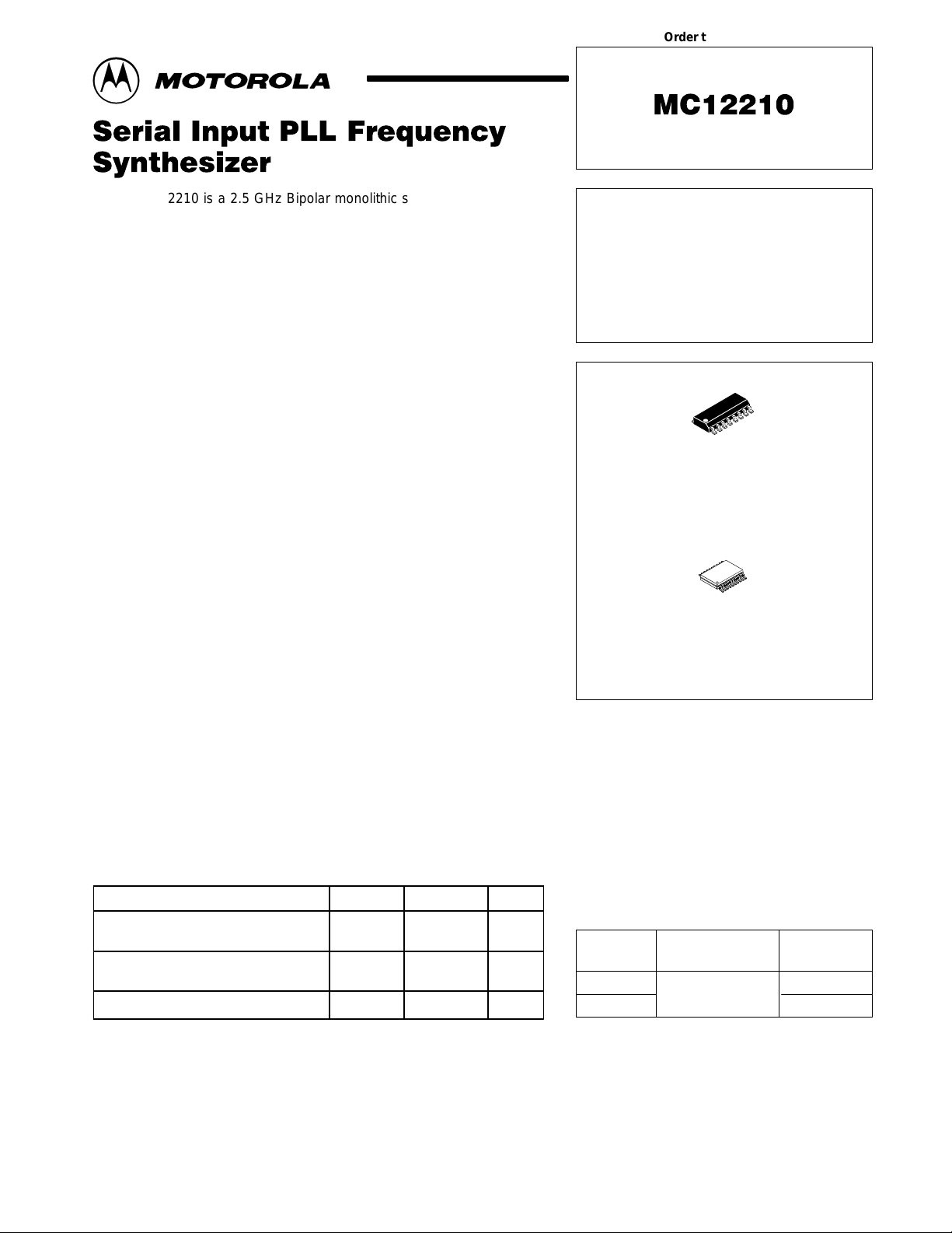
MECL PLL COMPONENTS
SERIAL PLL
FREQUENCY SYNTIESIZER
SEMICONDUCTOR
TECHNICAL DATA
16
1
D SUFFIX
PLASTIC PACKAGE
CASE 751B
(SO–16)
20
1
DT SUFFIX
PLASTIC PACKAGE
CASE 948E
(TSSOP–20)
MOSAIC V, Mfax and
MAXIMUM RATINGS
Parameter Symbol Value Unit
Power Supply Voltage, Pin 4 (Pin 5 in
20–lead package)
Power Supply Voltage, Pin 3 (Pin 4 in
20–lead package)
Storage Temperature Range Tstg –65 to 150 °C
NOTES: 1. Maximum Ratings are those values beyond which damage to the device may
occur. Functional operation should be restricted to the Recommended
Operating Conditions.
2.ESD data available upon request.
InterActiveApNote
(Note 1)
are trademarks of Motorola, Inc.
V
CC
V
p
–0.5 to 6.0 Vdc
VCC to 6.0 Vdc
ORDERING INFORMATION
Operating
Device
MC12210D
MC12210DT
Motorola, Inc. 1997 Rev 4
Temperature Range
TA = – 40° to +85°C
Package
SO–16
TSSOP–20
Page 2
MC12210
φ
R
φ
P
f
BISW
FC
LE
DATA
OUT
16
15
14
13
12
11
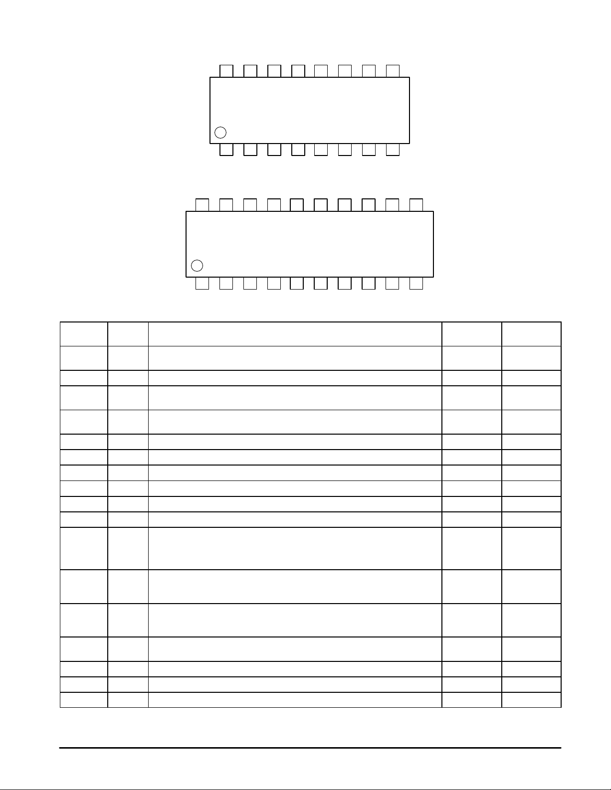
Pinout: 16–Lead Package (Top View)
1
2
3
4
5
6
OSCin
φ
20
OSCout
R
NC
19
φ
18
V
V
Do
FC
15
GND
LE
14
P
CC
P
f
BISW
OUT
17
16
Pinout: 20–Lead Package (Top View)
1
2
3
4
5
6
7
OSCin
NC
OSCout
V
V
Do
P
CC
GND
PIN NAMES
Pin I/O Function
OSCin I Oscillator input. A crystal may be connected between OSCin and OSCout. It is
OSCout O Oscillator output. Pin should be left open if external source is used 2 3
V
P
V
CC
Do O Internal charge pump output. Do remains on at all times 5 6
GND — Ground 6 7
LD O Lock detect, phase comparator output 7 8
f
IN
CLK I Clock input. Rising edge of the clock shifts data into the shift registers 9 11
DATA I Binary serial data input 10 13
LE I Load enable input (with internal pull up resistor). When LE is HIGH or OPEN, data
FC I Phase control select (with internal pull up resistor). When FC is LOW, the
BISW O Analog switch output. When LE is HIGH or OPEN (“analog switch is ON”) the
f
OUT
φP O Output for external charge pump. Standard CMOS output level 15 18
φR O Output for external charge pump. Standard CMOS output level 16 20
NC — No connect — 2, 9, 12, 19
highly recommended that an external source be ac coupled into this pin (see text).
— Power supply for charge pumps (VP should be greater than or equal to VCC) V
provides power to the Do, BISW and φP outputs
— Power supply voltage input. Bypass capacitors should be placed as close as
possible to this pin and be connected directly to the ground plane.
I Prescaler input. The VCO signal is AC–coupled into this pin 8 10
stored in the shift register is transferred into the appropriate latch (depending on
the level of control bit). Also, when LE is HIGH or OPEN, the output of the second
internal charge pump is connected to the BISW pin
characteristics of the phase comparator and charge pump are reversed. FC also
selects fp or fr on the f
output of the second charge pump is connected to the BISW pin. When LE is LOW,
BISW is high impedance
O Phase comparator input signal. When FC is HIGH, f
reference divider output; when FC is LOW, f
OUT
pin
=fp, programmable divider output
OUT
OUT
CLK
10
9
7
8
LD
f
IN
DATA
NC
CLK
13
12
11
8
9
10
LD
NC
f
=fr, programmable
IN
16–Lead Pkg
P
Pin No.
1 1
3 4
4 5
11 14
12 15
13 16
14 17
20–Lead Pkg
Pin No.
2
MOTOROLA RF/IF DEVICE DATA
Page 3
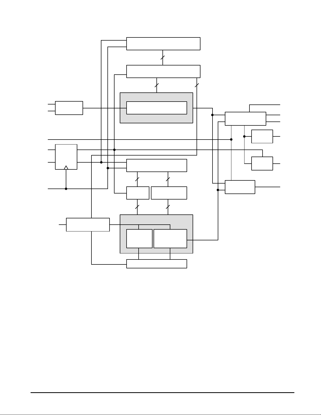
OSCin
OSCout
CRYST AL
OSCILLA TOR
MC12210
Figure 1. MC12210 Block Diagram
15–BIT SHIFT REGISTER
15
15–BIT LATCH
14 1
PROGRAMMABLE REFERENCE DIVIDER
14–BIT REFERENCE COUNTER
fr
PHASE/FREQUENCY
DETECTOR
LD
φ
φ
P
R
FC
LE
DATA
CLK
CONTROL
BIT
f
IN
LE
DATA
PRESCALER
32/33 or 64/65
18–BIT SHIFT REGISTER
7 11
7–BIT
LATCH
7 11
PROGRAMMABLE DIVIDER
7–BIT
SWALLOW
A–COUNTER
11–BIT LATCH
11–BIT
PROGRAMMABLE
N–COUNTER
CONTROL LOGIC
CHARGE
PUMP 1
CHARGE
PUMP 2
DIVIDER
OUTPUT MUX
fp
Do
BISW
f
OUT
MOTOROLA RF/IF DEVICE DATA
3
Page 4
MC12210
DATA ENTRY FORMAT
The three wire interface of DATA pin, CLK (clock) pin and LE (load enable) pin controls the serial data input of the 14–bit
programmable reference divider plus the prescaler setting bit, and the 18–bit programmable divider. A rising edge of the clock
shifts one bit of serial data into the internal shift registers. Depending upon the level of the control bit, stored data is transferred
into the latch when load enable pin is HIGH or OPEN.
Control bit: “H” = data is transferred into 15–bit latch of programmable reference divider
“L” = data is transferred into 18–bit latch of programmable divider
WARNING: Switching CLK or DA TA after the device is programmed may generate noise on the charge pump outputs which will
affect the VCO.
PROGRAMMABLE REFERENCE DIVIDER
16–bit serial data format for the programmable reference counter, “R–counter”, and prescaler select bit (SW) is shown below. If
the control bit is HIGH, data is transferred from the 15–bit shift register into the 15–bit latch which specifies the R divide ratio (8 to
16383) and the prescaler divide ratio (SW=0 for ÷64/65, SW=1 for ÷
For Control bit (C) = HIGH:
32/33). An R divide ratio less than 8 is prohibited.
SETTING BIT FOR PRESCALER DIVIDE RATIO (FIRST BIT)
MSB
R
R
R
R
R
R
R
S
8
9
10
11
12
13
14
W
SETTING BITS FOR DIVIDE RATIO OF PROGRAMMABLE
REFERENCE COUNTER (R–COUNTER)
R
R
R
5
6
7
CONTROL BIT (LAST BIT)
R
R
R
2
3
4
LSB
CR
1
DIVIDE RATIO OF PROGRAMMABLE REFERENCE (R) COUNTER
Divide
Ratio R
8 0 0 0 0 0 0 0 0 0 0 1 0 0 0
9 0 0 0 0 0 0 0 0 0 0 1 0 0 1
• • • • • • • • • • • • • • •
16383 1 1 1 1 1 1 1 1 1 1 1 1 1 1
14
R
13
R
12
R
R
11
10
R
R
9
R
8
R
7
R
6
R
5
R
4
R
3
R
2
PRESCALER SELECT BIT
Prescaler Divide Ratio P SW
64/65 0
32/33 1
R
1
4
MOTOROLA RF/IF DEVICE DATA
Page 5

MC12210
PROGRAMMABLE DIVIDER
19–bit serial data format for the programmable divider is shown below. If the control bit is LOW , data is transferred from the 18–bit
shift register into the 18–bit latch which specifies the swallow A–counter divide ratio (0 to 127) and the programmable N–counter
divide ratio (16 to 2047). An N–counter divide ratio less than 16 is prohibited.
For Control bit (C) = LOW:
MSB (FIRST BIT) CONTROL BIT (LAST BIT)
LSB
CA
1
18
A
A
A
A
A
A
N
N
N
N
N
N
N
N
N
N
N
2
3
4
5
6
7
8
9
10
11
12
13
14
15
16
17
SETTING BITS FOR
DIVIDE RATIO OF
PROGRAMMABLE N–COUNTER
SETTING BITS FOR
DIVIDE RATIO OF
SWALLOW A–COUNTER
DIVIDE RATIO OF PROGRAMMABLE N–COUNTER DIVIDE RATIO OF SWALLOW A–COUNTER
Divide
Ratio NN18N17N16N15N14N13N12N11N10N9N8
16 0 0 0 0 0 0 1 0 0 0 0 0 0 0 0 0 0 0 0
17 0 0 0 0 0 0 1 0 0 0 1 1 0 0 0 0 0 0 1
• • • • • • • • • • • • • • • • • • • •
2047 1 1 1 1 1 1 1 1 1 1 1 127 1 1 1 1 1 1 1
Divide
Ratio AA7A6A5A4A3A2A1
DIVIDE RATIO SETTING
fvco = [(P•N)+A]•fosc ÷ R with A<N
fvco: Output frequency of external voltage controlled oscillator (VCO)
N: Preset divide ratio of binary 11–bit programmable counter (16 to 2047)
A: Preset divide ratio of binary 7–bit swallow counter (0 to 127, A<N)
fosc: Output frequency of the external frequency oscillator
R: Preset divide ratio of binary 14–bit programmable reference counter (8 to 16383)
P: Preset mode of dual modulus prescaler (32 or 64)
DATA
CLK
LE
N18:MSB N17
(SW:MSB) (R14)
ts(D) th(D) t
NOTES:Programmable reference divider data shown in parenthesis. Data shifted into register on rising edge of CLK.
ts(D) = Setup Time DATA to CLK ts(D)
th(D) = Hold Time DATA to CLK th(D)
tCW = CLK Pulse Width tCW
tEW = LE Pulse Width tEW
ts(C
→
LE) = Setup Time CLK to LE ts(C→LE) ≥30 ns
MOTOROLA RF/IF DEVICE DATA
Figure 2. Serial Data Input Timing
N8 A7
(R7) (R6)
CW
≥
10 ns
≥
20 ns
≥
30 ns
≥
20 ns
A1 C = CONTROL BIT (LAST BIT)
(R1) (C = CONTROL BIT (LAST BIT))
ts(C→LE)
t
EW
5
Page 6

MC12210
PHASE CHARACTERISTICS/VCO CHARACTERISTICS
The phase comparator in the MC12210 is a high speed digital phase frequency detector circuit. The circuit determines the “lead”
or “lag” phase relationship and time difference between the leading edges of the VCO (fp) signal and the reference (fr) input.
Since these edges occur only once per cycle, the detector has a range of ±2π radians. The phase comparator outputs are
standard CMOS rail–to–rail levels (VP to GND for φP and VCC to GND for φR), designed for up to 20MHz operation into a 15pF
load. These phase comparator outputs can be used along with an external charge pump to enhance the PLL characteristics.
The operation of the phase comparator is shown in Figures 3 and 5. The phase characteristics of the phase comparator are
controlled by the FC pin. The polarity of the phase comparator outputs, φR and φP, as well as the charge pump output Do can be
reversed by switching the FC pin.
Figure 3. Phase/Frequency Detector, Internal Charge Pump and Lock Detect Waveforms
H
fr
L
H
fp
L
H
LD
L
Do (FC = H)
BISW (LE = H or Open)
φ
R (FC = H)
φ
P (FC = H)
Do (FC = L)
BISW (LE = H or Open)
φ
R (FC = L)
φ
P (FC = L)
NOTES: Do and BISW are current outputs.
Source
Z
Sink
H
L
H
L
Source
Z
Sink
H
L
H
L
Phase difference detection range: –2
Spike difference depends on charge pump characteristics. Also, the spike is output in order to diminish dead band.
When fr > fp or fr < fp, spike might not appear depending upon charge pump characteristics.
π
to +2
π
I
)
source
Internal Charge Pump Gain
Ť
[
6
I
sink
4
p
4mA
Ť
+
4
p
MOTOROLA RF/IF DEVICE DATA
Page 7

MC12210
For FC = HIGH:
fr lags fp in phase OR fp>fr in frequency
When the phase of fr lags that of fp or the frequency of fp is greater than fr, the φP output will remain in a HIGH state while the φR
output will pulse from LOW to HIGH. The output pulse will reach a minimum 50% duty cycle under a 180° out of phase condition.
The signal on φR indicates to the VCO to decrease in frequency to bring the loop into lock.
fr leads fp in phase OR fp<fr in frequency
When the phase of fr leads that of fp or the frequency of fp is less than fr, the φR output will remain in a LOW state while the φP
output pulses from HIGH to LOW. The output pulse will reach a minimum 50% duty cycle under a 180° out of phase condition.
The signal on φP indicates to the VCO to increase in frequency to bring the loop to lock.
fr = fp in phase and frequency
When the phase and frequency of fr and fp are equal, the output φP will remain in a HIGH state and φR will remain in a LOW state
except for voltage spikes when signals are in phase. This situation indicates that the loop is in lock and the phase comparator will
maintain the loop in its locked state.
When FC = LOW, the operation of the phase comparator is reversed from the above explanation.
For FC = LOW:
fr lags fp in phase OR fp>fr in frequency
When the phase of fr lags that of fp or the frequency of fp is greater than fr, the φR output will remain in a LOW state while the φP
output will pulse from HIGH to LOW. The output pulse will reach a minimum 50% duty cycle under a 180° out of phase condition.
The signal on φP indicates to the VCO to increase in frequency to bring the loop into lock.
fr leads fp in phase OR fp<fr in frequency
When the phase of fr leads that of fp or the frequency of fp is less than fr, the φP output will remain in a HIGH state while the φR
output pulses from LOW to HIGH. The output pulse will reach a minimum 50% duty cycle under a 180° out of phase condition.
The signal on φR indicates to the VCO to decrease in frequency to bring the loop to lock.
fr = fp in phase and frequency
When the phase and frequency of fr and fp are equal, the output φP will remain in a HIGH state and φR will remain in a LOW state
except for voltage spikes when signals are in phase. This situation indicates that the loop is in lock and the phase comparator will
maintain the loop in its locked state.
The FC pin controls not only the phase characteristics, but also controls the f
either of the phase comparator input signals, fr or fp, at the f
output providing a test mode where the programming of the
OUT
dividers and the output of the counters can be checked. When FC is HIGH, f
When FC is LOW, f
= fp, the programmable divider output.
OUT
Hence,
If VCO characteristics are like (1), FC should be set HIGH or OPEN. f
If VCO characteristics are like (2), FC should be set LOW. f
Figure 4. VCO Characteristics
Figure 5. Phase Comparator, Internal Charge Pump, and
( 1 )
fp < fr H L L fr L H H fp
fp > fr L H H fr H L L fp
fp = fr Z L H fr Z L H fp
VCO OUTPUT FREQUENCY
( 2 )
VCO INPUT VOLTAGE
NOTES:Z = High impedance
test pin. The FC pin permits the user to monitor
OUT
= fr, the programmable reference divider output.
OUT
= fr
OUT
= fp
OUT
f
Characteristics
OUT
FC = HIGH or OPEN FC = LOW
Do φR φP f
When LE is HIGH or Open, BISW has the same
characteristics as Do.
Do φR φP f
OUT
OUT
MOTOROLA RF/IF DEVICE DATA
7
Page 8

MC12210
Figure 6. Detailed Phase Comparator Block Diagram
UP
DOWN
CHARGE
PUMP 1
CHARGE
PUMP 2
φ
P
φ
R
LD
Do
BISW
FC
LE
fr
fp
0
1
0
1
R
PHASE
FREQUENCY
DETECTOR
V
PHASE COMPARATOR
LOCK DETECT
The Lock Detect (LD) output pin provides a LOW pulse when fr and fp are not equal in phase or frequency . The output is normally
HIGH. LD is designed to be the logical NORing of the phase frequency detector’s outputs UP and DOWN. See Figure 6. In typical
applications the output signal drives external circuitry which provides a steady LOW signal when the loop is locked. See Figure 9.
OSCILLATOR INPUT
For best operation, an external reference oscillator is recommended. The signal should be AC–coupled to the OSCin pin through
a coupling capacitor. In this case, no connection to OSCout is required. The magnitude of the AC–coupled signal must be
between 500 and 2200 mV peak–to–peak. To optimize the phase noise of the PLL when used in this mode, the input signal
amplitude should be closer to the upper specification limit. This maximizes the slew rate of the signal as it switches against the
internal voltage reference.
The device incorporates an on–chip reference oscillator/buffer so that an external parallel–resonant fundamental crystal can be
connected between OSCin and OSCout. External capacitor C1 and C2 as shown in Figure 10 are required to set the proper
crystal load capacitance and oscillator frequency. The values of the capacitors are dependent on the crystal chosen (up to a
maximum of 30 pF each including parasitic and stray capacitance). However, using the on–chip reference oscillator greatly
increases the synthesized phase noise.
DUAL INTERNAL CHARGE PUMPS (“ANALOG SWITCH”)
Due to the pure Bipolar nature of the MC12210 design, the “analog switch” function is implemented with dual internal charge
pumps. The loop filter time constant can be decreased by bypassing the first stage of the loop filter with the charge pump output
BISW as shown in Figure 7 below. This enables the VCO to lock in a shorter amount of time.
When LE is HIGH or OPEN (“analog switch is ON”), the output of the second internal charge pump is connected to the BISW pin,
and the Do output is ON. The charge pump 2 output on BISW is essentially equal to the charge pump 1 output on Do. When LE is
LOW, BISW is in a high impedance state and Do output is active.
Figure 7. “Analog Switch” Block Diagram
CHARGE
PUMP 1
Do
LPF–1 LPF–2 VCO
CHARGE
PUMP 2
LE
8
BISW
MOTOROLA RF/IF DEVICE DATA
Page 9

MC12210
ELECTRICAL CHARACTERISTICS (V
Parameter
Supply Current for V
Supply Current for V
Operating Frequency fINmax
Operating Frequency (OSCin) F
Input Sensitivity f
Input HIGH Voltage CLK, DATA, LE, FC V
Input LOW Voltage CLK, DATA, LE, FC V
Input HIGH Current (DATA and CLK) I
Input LOW Current (DATA and CLK) I
Input Current (OSCin) I
Input HIGH Current (LE and FC) I
Input LOW Current (LE and FC) I
Charge Pump Output Current I
Do and BISW I
Output HIGH Voltage (LD, φR, φP, f
Output LOW Voltage (LD, φR, φP, f
Output HIGH Current (LD, φR, φP, f
Output LOW Current (LD, φR, φP, f
1. VCC = 3.3 V, all outputs open. 4. Vp = 6.0 V, all outputs open.
2. VCC = 5.5 V, all outputs open. 5. AC coupling, FIN measured with a 1000 pF capacitor.
3. VP = 3.3 V , all outputs open. 6. Source current flows out of the pin and sink current flows into the pin.
CC
P
OUT
OUT
OUT
OUT
= 2.7 to 5.5 V; TA = –40 to +85°C, unless otherwise noted.)
CC
Symbol Min Typ Max Unit Condition
fINmin
IN
OSCin V
)
)
)
)
I
CC
I
P
F
IN
OSC
V
IN
OSC
IH
IL
IH
IL
OSC
IH
IL
Source
Sink
I
Hi–Z
V
OH
V
OL
I
OH
I
OL
6
6
– 8.8 13.0 mA Note 1
– 10.2 16.0 Note 2
– 0.7 1.1 mA Note 3
– 0.8 1.3 Note 4
2500
–
– 12 20 MHz Crystal Mode
– – 40 MHz External Reference Mode
200 – 1000 mVpp
500 – 2200 mVpp
0.7 V
CC
– – 0.3 V
– 1.0 2.0 µA VCC = 5.5 V
–10 –5.0 – µA VCC = 5.5 V
–
–
– 1.0 2.0 µA
–75 –60 – µA
–2.6 –2.0 –1.4 mA VDo = Vp/2; Vp = 2.7 V
+1.4 +2.0 +2.6 V
–15 – +15 nA 0.5< VDO < Vp – 0.5
4.4 – – V VCC = 5.0 V
2.4 – – V VCC = 3.0 V
– – 0.4 V VCC = 5.0 V
– – 0.4 V VCC = 3.0 V
–1.0 – – mA
1.0 – – mA
–
–
– – V
130
–310
–
500
–
–
CC
MHz Note 5
V VCC = 5.5 V
µA OSCin = V
OSCin = VCC – 2.2 V
BISW
0.5 < V
CC
= Vp/2; Vp = 2.7 V
< Vp – 0.5
BISW
Figure 8. T ypical External Charge Pump Circuit
V
p
10 k
Ω
12 k
12 k
Ω
EXTERNAL CHARGE
PUMP OUTPUT
Ω
10 k
Ω
φ
P
φ
R
MOTOROLA RF/IF DEVICE DATA
Figure 9. T ypical Lock Detect Circuit
V
CC
100 k
Ω
33 k
LD
Ω
0.01 µF
10 k
Ω
LOCK DETECT
OUTPUT
9
Page 10

MC12210
Figure 10. T ypical Applications Example (16–Pin Package)
LOCK
DETECT
C1
C2
V
P
100 pF
V
CC
100 pF
LOCK DETECT
CIRCUIT
(SEE FIGURE 9)
1
2
3
0.1 µF
4
0.1 µF
5
6
7
8
1000 pF
OSCin
OSCout
V
P
V
CC
Do
GND
LD
f
in
MC12210
φ
R
φ
P
FOUT
BISW
FC
LE
DATA
CLK
16
CHARGE PUMP
(SEE FIGURE 8)
15
14
13
12
11
10
9
47 k
EXTERNAL
(SEE FIGURE 11)
CHARGE PUMP SELECTION
(INTERNAL OR EXTERNAL)
FROM
47 k
Ω
Ω
CONTROLLER
LOW PASS
FILTER
VCO
BISW
Do OR EXTERNAL
CHARGE PUMP
C1, C2: Dependent on Crystal Oscillator
Figure 11. Typical Loop Filter
VCO
R
C
10
MOTOROLA RF/IF DEVICE DATA
Page 11

–T
SEATING
–
PLANE
MC12210
OUTLINE DIMENSIONS
D SUFFIX
–A
–
916
–B
1
–
8
G
K
D
16 PL
0.25 (0.010) T B A
M
S S
PLASTIC PACKAGE
CASE 751B–05
P 8 PL
0.25 (0.010) B
C
PLASTIC PACKAGE
CASE 948E–02
(SO–16)
ISSUE J
M M
R X 45°
M
DT SUFFIX
(TSSOP–20)
ISSUE A
NOTES:
1. DIMENSIONING AND TOLERANCING PER ANSI
Y14.5M, 1982.
2. CONTROLLING DIMENSION: MILLIMETER.
3. DIMENSIONS A AND B DO NOT INCLUDE
MOLD PROTRUSION.
4. MAXIMUM MOLD PROTRUSION 0.15 (0.006)
PER SIDE.
5. DIMENSION D DOES NOT INCLUDE DAMBAR
PROTRUSION. ALLOWABLE DAMBAR
PROTRUSION SHALL BE 0.127 (0.005) TOTAL
IN EXCESS OF THE D DIMENSION AT
MAXIMUM MATERIAL CONDITION.
MILLIMETERS INCHES
MIN MINMAX MAX
DIM
A
F
J
9.80
B
3.80
C
1.35
D
0.35
F
0.40
1.27 BSC 0.050 BSC
G
J
0.19
K
0.10
M
0
°
P
5.80
R
0.25
10.00
4.00
1.75
0.49
1.25
0.25
0.25
7
6.20
0.50
0.386
0.393
0.150
0.157
0.054
0.068
0.014
0.019
0.016
0.049
0.008
0.009
0.004
0.009
0
7
°
°
0.229
0.010
0.244
0.019
°
20X REFK
S
U0.15 (0.006) T
0.10 (0.004) V
M
S
U
T
S
K
2X
L/2
L
PIN 1
IDENT
110
1120
B
JJ1
–U–
N
S
U0.15 (0.006) T
A
K1
SECTION N–N
0.25 (0.010)
M
–V–
N
F
DETAIL E
C
G
H
DETAIL E
0.100 (0.004)
SEATING
–T–
PLANE
D
NOTES:
1 DIMENSIONING AND TOLERANCING PER ANSI
Y14.5M, 1982.
2 CONTROLLING DIMENSION: MILLIMETER.
3 DIMENSION A DOES NOT INCLUDE MOLD FLASH,
PROTRUSIONS OR GATE BURRS. MOLD FLASH
OR GATE BURRS SHALL NOT EXCEED 0.15
(0.006) PER SIDE.
4 DIMENSION B DOES NOT INCLUDE INTERLEAD
FLASH OR PROTRUSION. INTERLEAD FLASH OR
PROTRUSION SHALL NOT EXCEED 0.25 (0.010)
PER SIDE.
5 DIMENSION K DOES NOT INCLUDE DAMBAR
PROTRUSION. ALLOWABLE DAMBAR
PROTRUSION SHALL BE 0.08 (0.003) TOTAL IN
EXCESS OF THE K DIMENSION AT MAXIMUM
MATERIAL CONDITION.
6 TERMINAL NUMBERS ARE SHOWN FOR
REFERENCE ONLY.
7 DIMENSION A AND B ARE TO BE DETERMINED
AT DATUM PLANE –W–.
INCHES
6.60 0.260
–W–
MILLIMETERS
DIMAMIN MAX MIN MAX
6.40 0.252
B 4.30 4.50 0.169 0.177
C 1.20 0.047
––– –––
D 0.05 0.15 0.002 0.006
F 0.50 0.75 0.020 0.030
G 0.65 BSC 0.026 BSC
H 0.27 0.37 0.011 0.015
J 0.09 0.20 0.004 0.008
J1 0.09 0.16 0.004 0.006
K 0.19 0.30 0.007 0.012
K1 0.19 0.25 0.007 0.010
L 6.40 BSC 0.252 BSC
M 0 8 0 8
____
MOTOROLA RF/IF DEVICE DATA
11
Page 12

MC12210
Motorola reserves the right to make changes without further notice to any products herein. Motorola makes no warranty , representation or guarantee regarding
the suitability of its products for any particular purpose, nor does Motorola assume any liability arising out of the application or use of any product or circuit, and
specifically disclaims any and all liability, including without limitation consequential or incidental damages. “T ypical” parameters which may be provided in Motorola
data sheets and/or specifications can and do vary in different applications and actual performance may vary over time. All operating parameters, including “Typicals”
must be validated for each customer application by customer’s technical experts. Motorola does not convey any license under its patent rights nor the rights of
others. Motorola products are not designed, intended, or authorized for use as components in systems intended for surgical implant into the body, or other
applications intended to support or sustain life, or for any other application in which the failure of the Motorola product could create a situation where personal injury
or death may occur. Should Buyer purchase or use Motorola products for any such unintended or unauthorized application, Buyer shall indemnify and hold Motorola
and its officers, employees, subsidiaries, affiliates, and distributors harmless against all claims, costs, damages, and expenses, and reasonable attorney fees
arising out of, directly or indirectly, any claim of personal injury or death associated with such unintended or unauthorized use, even if such claim alleges that
Motorola was negligent regarding the design or manufacture of the part. Motorola and are registered trademarks of Motorola, Inc. Motorola, Inc. is an Equal
Opportunity/Affirmative Action Employer.
How to reach us:
USA/EUROPE/ Locations Not Listed: Motorola Literature Distribution; JAPAN: Nippon Motorola Ltd.: SPD, Strategic Planning Office, 141,
P.O. Box 5405, Denver, Colorado 80217. 1–303–675–2140 or 1–800–441–2447 4–32–1 Nishi–Gotanda, Shagawa–ku, Tokyo, Japan. 03–5487–8488
Customer Focus Center: 1–800–521–6274
Mfax: RMFAX0@email.sps.mot.com – TOUCHTONE 1–602–244–6609 ASIA/PACIFIC: Motorola Semiconductors H.K. Ltd.; 8B T ai Ping Industrial Park,
Moto rola Fax Back Sys tem – US & Canada ONLY 1–800–774–1848 51 Ting Kok Road, Tai Po, N.T., Hong Kong. 852–26629298
HOME PAGE: http://motorola.com/sps/
12
– http://sps.motorola.com/mfax/
◊
Mfax is a trademark of Motorola, Inc.
MOTOROLA RF/IF DEVICE DATA
MC12210/D
 Loading...