

Page 1
The MC12181 is a monolithic bipolar synthesizer integrating a high
performance prescaler, programmable divider, phase/frequency detector,
charge pump, and reference oscillator/buffer functions. The device is
capable of synthesizing a signal which is 25 to 40 times the input reference
signal. The device has a 4–bit parallel interface to set the proper total
multiplication which can range from 25 to 40. When combined with an
external passive loop filter and VCO, the MC12181 serves as a complete
PLL subsystem.
• 2.7 to 5.5 V Operation
• Low power supply current of 4.25 mA typical
• On chip reference oscillator/buffer supporting wide frequency operating
range from 5 to 25 MHz
• 4–bit parallel interface for programming divider (N = 25 .... 40)
• Wide 125 – 1000 MHz frequency of operation
• Digital phase/frequency detector with linear transfer function
• Balanced Charge Pump Output
• Space efficient 16 lead SOIC package
• Operating Temperature Range of –40 to 85°C
• > 1000 V ESD Protection (I/O to Ground, I/O to V
The device is suitable for applications where a fixed local oscillator (LO)
needs to be synthesized or where a limited number of LO frequencies need
to be generated. The device also has auxiliary open emitter outputs (Pout
and Rout) for observing the inputs to the phase detector for verification
purposes. In normal use the pins should be left open. The Reset input is
normally LOW. When this input is placed in the HIGH state the reference
prescaler is reset and the charge pump output (Do) is placed in the OFF
state.
The 4–bit programming interface maps into divider states ranging from 25
to 40. A is the LSB and D is the MSB. The data inputs (A,B,C, and D) are
CMOS compatible and have pull–up resistors. The inputs can be tied directly
to Vcc or Ground for programming or can be interfaced to an external data
latch/register. Table 1 below has a mapping of the programming states.
T able 1. Programming States
D C B A Divider
L L L L 25
L L L H 26
L L H L 27
L L H H 28
L H L L 29
L H L H 30
L H H L 31
L H H H 32
H L L L 33
H L L H 34
H L H L 35
H L H H 36
H H L L 37
H H L H 38
H H H L 39
H H H H 40
CC
)
Order this document by MC12181/D
125 – 1000 MHZ
FREQUENCY SYNTHESIZER
SEMICONDUCTOR
TECHNICAL DATA
16
1
D SUFFIX
PLASTIC PACKAGE
CASE 751B
(SO–16)
PIN CONNECTIONS
AOSCin
161
BOSCout
152
CV
P
CC
(Top View)
ORDERING INFORMATION
Operating
Device
MC12181D TA = –40° to +85°C SO–16
Temperature Range
143
134
125
116
107
98
DV
PoutDo
ResetGND
RoutFin
GNDFin
Package
Motorola, Inc. 1997 Rev 2
Page 2
MC12181
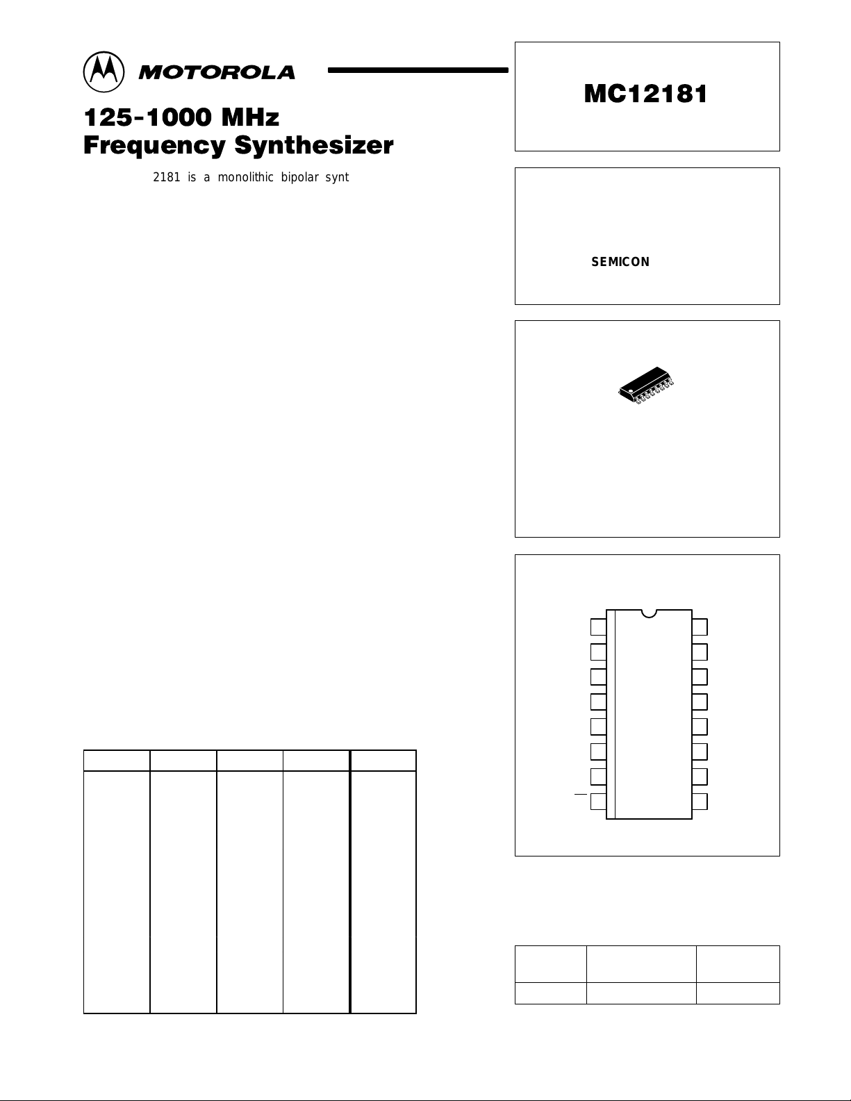
Figure 1. MC12181 Programmable Synthesizer
ABCD
DECODE
LOGIC
Fin
Fin
Reset
OSCin
OSCout
DIVIDE BY 8
PRESCALER
CRYSTAL
OSCILLA T OR/BUFFER
PROGRAMMABLE
DIVIDER (25 – 40)
DIVIDE BY 8
PRESCALER
PHASE/FREQ
DETECTOR
DIVIDE
BY 2
CHARGE
PUMP
Pout
Do
Rout
PIN NAMES
Pin No. Pin Function
1 OSCin An external parallel resonant, fundamental crystal is connected between OSCin and OSCout to form an internal
2 OSCout Oscillator output, for use with an external crystal as shown in Figure 2.
3 V
4 V
5 Do Single ended phase/frequency detector output. Three–state current sink/source output for use as a loop error
6 GND Ground. This pin should be directly tied to the ground plane.
7 Fin Prescaler input – The VCO signal is ac–coupled into the Fin Pin.
8 Fin Complementary prescaler input – This pin should be capacitively coupled to ground.
9 GND Ground. This pin should be directly tied to the ground plane.
10 Rout Open emitter test point used to verify proper operation of the reference divider chain. In normal operation this pin
11 Reset Test pin used to clear the prescalers (Reset = H). When the Reset is in the HIGH state, the charge pump output
12 Pout Open emitter test point used to verify proper operation of the programmable divider chain. The output is a
13
14
15
16
CC
D
C
B
A
reference crystal oscillator. External capacitors C1 and C2 are required to set the proper crystal load capacitance
and oscillator frequency (Figure 2). For an external reference oscillator, a signal is ac–coupled into the OSCin pin.
In either mode a 50 kΩ resistor MUST be connected between OSCin and OSCout.
Positive power supply for charge pump. VP MUST be greater than or equal to VCC. Bypassing should be placed
P
as close as possible to this pin and be connected directly to the ground plane.
Positive power supply. Bypassing should be placed as close as possible to this pin and be connected directly to
the ground plane.
signal when combined with an external low pass filter. The phase/frequency detector is characterized by a linear
transfer function.
should be left OPEN.
is disabled. The Reset input has an internal pulldown. In normal operation it can be left open or tied to ground.
divide–by–2 version of the programmable input to the phase/frequency detector. In normal operation this pin
should be left OPEN.
Digital control inputs for setting the value of the programmable divider. A is the LSB and D is the MSB. In normal
operation these pins can be tied to VCC and/or ground to program a fixed divide or they can be driven by a CMOS
logic level when used in a programmable mode. There is an internal pull–up resistor to VCC on each input.
2
MOTOROLA RF/IF DEVICE DATA
Page 3
R1 is 50 k
Ω
C1/C2 depend on crystal selected
(Nominal)
Passive
Filter
V
P
0.1 µF 100 pF
V
CC
0.1 µF 100 pF
C1
C2
MC12181
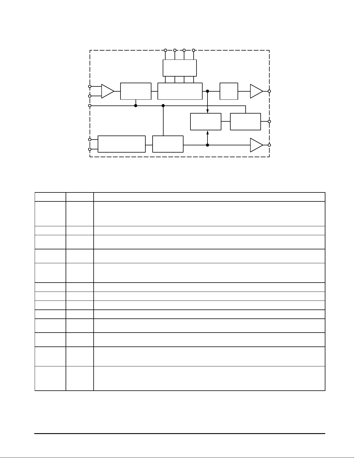
Figure 2. T ypical Applications Example
OSCin
R1
OSCout B
V
P
V
CC
Do
Pout
A
161
152
C
143
D
134
125
CMOS Logic
Levels or V
and/or GND
NC
CC
VCO
GND Reset
1000 pF
Fin Rout
1000 pF
Fin
GND
116
NC
107
98
Figure 3. T ypical Passive Loop Filter Topology
R
Do
X
R
O
C
O
C
A
C
VCO Input
X
RECOMMENDED OPERATING CONDITIONS
Parameter Symbol Min Max Unit
Supply Range V
Maximum Supply Range VCCmax – –6.0 VDC
Maximum Charge Pump Voltage VPmax – VCC to +6.0 VDC
T emperature Ambient T
Storage Temperature T
Maximum Input Signal (Any Pin) Vinmax – VCC+0.5 V VDC
CC
A
STG
2.7 5.5 VDC
–40 85 °C
–65 150 °C
MOTOROLA RF/IF DEVICE DATA
3
Page 4

MC12181
ELECTRICAL CHARACTERISTICS (V
Characteristic
Supply Current for V
Supply Current for V
Input Frequency Range OSCin 5 – 25 MHz Note 2
RF Input Frequency Range Fin 125 – 1000 MHz Note 3
Fin Input Sensitivity Vin 100 – 1000 mVpp Note 4
OSCin Input Sensitivity V
Output Source Current (Do) I
Output Sink Current (Do) I
Output Leakage Current (Do) I
Charge Pump Operating Volt VDo 0.5 – VP–0.5 V
Input HIGH Voltage Reset, A, B, C, D V
Input LOW Voltage Reset, A, B, C, D V
Input HIGH Current A, B, C, D I
Input LOW Current A, B, C, D I
Output Amplitude (Pout, Rout) Vout 250 400 – mVpp Note 7
NOTES: 1. VCC and VP = 5.5 V; Fin = 1.0 GHz; OSCin = 25 MHz; Do open.
2.Assumes C1 and C2 (Figure 2) limited to ≤30 pF each including stray capacitance in crystal mode, ac coupled input for external reference mode.
3.AC coupling, Fin measured with a 1000pF capacitor.
4.Signal ac coupling in input.
5.VCC = 5.5 V; VP = 6.0 V; VDO = 3.0 V.
6.VP = VCC = 3.0 V; VDO = 1.5 V.
7.Minimum resistor value of 25 kΩ to ground.
CC
P
Reset – – +100
Reset –1 – +1
= 2.7 to 5.5 V; VP = VCC to 6.0 V; TA = –40 to +85°C, unless otherwise noted.)
CC
Symbol Min Typ Max Unit Condition
I
CC
I
P
OSC
OH
OL
OZ
IH
IL
IH
IL
– 4.0 5.5 mA Note 1
– 0.25 0.5 mA Note 1
500 – 2200 mVpp Note 4
–2.8 –2.2 –2.0 mA Note 5
–2.4 –2.0 –1.6 Note 6
2.0 2.4 2.8 mA Note 5
1.6 2.0 2.4 Note 6
– 0.5 10 nA VCC=5.5; VP = 6.0 V;
0.7 V
CC
– – 0.3 V
– – +1 µA
–100 – – µA
– – V
CC
VDo=0.5 to 5.5 V
V
4
MOTOROLA RF/IF DEVICE DATA
Page 5

MC12181
APPLICATIONS INFORMATION
The MC12181 is intended for applications where a fixed
LO, or a limited number of local oscillator frequencies is
required to be synthesized. The device acts as a x25 – 40
PLL. The 4–bit parallel interface allows 1 of 16 divide ratios to
be selected. Internally there are fixed divide by 8 prescalers
in the reference and programmable paths of the PLL. The
MC12181 operates from 125 MHz to 1000 MHz which makes
the part ideal for FCC Title 47; Part 15 applications in the 260
MHz to 470 MHz band and the 902 to 928 MHz Band.
Figure 4 shows a typical block diagram of the application.
Figure 4. T ypical Block Diagram of Complete PLL
External
Ref
10.0MHz
MC12181 PLL
φ
÷
8
/Freq
Det
÷
N
25–40
Charge
Pump
÷
8
Loop
Filter
VCO
250–400
MHz
As can be seen from the block diagram, with the addition
of a VCO, a loop filter, and either an external oscillator or
crystal, a complete PLL sub–system can be realized. Since
most of the PLL functions are integrated into the 12181, the
users focus is on the loop filter design and the crystal
reference oscillator circuit.
Crystal Oscillator Design
The PLL is used to transfer the high stability characteristic
of a low frequency reference source to the high frequency
VCO within the PLL loop. To facilitate this, the device
contains an input circuit which can be configured as a crystal
oscillator or a buffer for accepting an external signal source.
In the external reference mode, the reference source is
ac–coupling into the OSCin input pin. The level of this signal
should be between 500 – 2200 mVp–p. An external low noise
reference should be used when it is desired to obtain the best
close–in phase noise performance for the PLL. In addition the
input reference amplitude should be close to the upper
amplitude specification. This maximizes the slew rate of the
input signal as it switches against the internal voltage
reference.
In the crystal mode, an external parallel–resonant
fundamental mode crystal should be connected between the
OSCin and OSCout pins. This crystal must be between 5 and
25 MHz. External capacitors C1 and C2, as shown in
Figure 2, are required to set the proper crystal load
capacitance and oscillator frequency. The values of the
capacitors are dependent on the crystal choosen and the
input capacitance of the device as well as stray board
capacitance.
Since the MC12181 is realized with an all–bipolar ECL
style design, the internal oscillator circuitry is different from
more traditional CMOS oscillator designs which realize the
crystal oscillator with a modified inverter topology. These
CMOS designs typically excite the crystal with a rail–to–rail
signal which may overdrive the crystal resulting in damage or
unstable operation. The MC12181 design does not exhibit
this phenomena because the swing out of the OSCout pin is
less than 600 mVp–p. This has the added advantage of
minimizing EMI and switching noise which can be generated
by rail–to–rail CMOS outputs. The OSCout output should not
be used to drive other circuitry.
The oscillator buffer in the MC12181 is a single stage, high
speed, differential input/output amplifier; it may be
considered to be a form of the Pierce oscillator. A simplified
circuit diagram is seen in Figure 5.
Figure 5. Simplified Crystal Oscillator/Buffer Circuit
V
CC
OSC
out
Bias
Source
OSC
in
To Phase/
Frequency
Detector
OSCin drives the base of one input of an NPN transistor
differential pair . The non–inverting input of the differential pair
is internally biased. OSC
is the inverted input signal and is
out
buffered by an emitter follower with a 70 µA pull–down
current and has a voltage swing of about 600mVp–p. Open
loop output impedance is approximately 425 Ω. The opposite
side of the differential amplifier output is used internally to
drive another buffer stage which drives the phase/frequency
detector. With the 50 kΩ feedback resistor in place, OSC
and OSC
are biased to approximately 1.1 V below VCC.
out
The amplifier has a voltage gain of about 15dB and a
bandwidth in excess of 150 MHz. Adherence to good RF
design and layout techniques, including power supply pin
decoupling, is strongly recommended.
A typical crystal oscillator application is shown in Figure 2.
The crystal and the feedback resistor are connected directly
between OSCin and OSC
, while the loading capacitors, C1
out
and C2, are connected between OSCin and ground, and
OSC
and ground respectively . It is important to understand
out
that as far as the crystal is concerned, the two loading
capacitors are in series (albeit through ground). So when the
crystal specification defines a specific loading capacitance,
this refers to the total external (to the crystal) capacitance
seen across its two pins.
This capacitance consists of the capacitance contributed
by the amplifier (IC and packaging), layout capacitance, and
the series combination of the two loading capacitors. This is
illustrated in the equation below:
CI+
C
AMP
)
C
STRAY
C1 C2
)
C1)C2
Provided the crystal and associated components are
located immediately next to the IC, thus minimizing the stray
capacitance, the combined value of C
AMP
and C
STRAY
is
approximately 5pF. Note that the location of the OSCin and
OSC
pins at the end of the package, facilitates placing the
out
crystal, resistor and the C1 and C2 capacitors very close to
the device. Usually , one of the capacitors is in parallel with an
adjustable capacitor used to trim the frequency of oscillation.
in
MOTOROLA RF/IF DEVICE DATA
5
Page 6

MC12181
It is important that the total external (to the IC) capacitance
seen by either OSCin or OSC
In operation, the crystal oscillator will start up with the
application of power. If the crystal is in a can that is not
grounded it is often possible to monitor the frequency of
oscillation by connecting an oscilloscope probe to the can;
this technique minimizes any disturbance to the circuit. If this
is not possible, a high impedance, low capacitance, FET
probe can be connected to either OSCin or OSC
typically seen at those points will be very nearly sinusoidal
with amplitudes of roughly 300–600mVp–p. Some distortion
is inevitable and has little bearing on the accuracy of the
signal going to the phase detector.
Loop Filter Design
Because the device is designed for a non–frequency agile
synthesizer (i.e., how fast it tunes is not critical) the loop filter
design is very straight forward. The current output of the
charge pump allows the loop filter to be realized without the
need of any active components. The preferred topology for
the filter is illustrated in Figure 6.
Figure 6. Loop Filter
Xtl
Osc
MC12181
Ph/Frq
÷
8
÷
25–40
Det
÷
Chrg
Pump
K
N
8
The Ro/Co components realize the primary loop filter. Ca is
added to the loop filter to provide for reference sideband
suppression. If additional suppression is needed, the Rx/C
realizes an additional filter. In most applications, this will not
be necessary. If all components are used, this results in a 4th
order PLL, which makes analysis difficult. To simplify this, the
loop design will be treated as a 2nd order loop (Ro/Co) and
additional guidelines are provided to minimize the influence
of the other components. If more rigorous analysis is needed,
mathematical/system simulation tools should be used.
Component Guideline
C
a
R
x
C
x
The focus of the design effort is to determine what the
loop’s natural frequency , ωo, should be. This is determined by
Ro, Co, Kp, Kv, and Nt. Because Kp, Kv, and Nt are given, it is
only necessary to calculate values for Ro and Co. There are
3 considerations in selecting the loop bandwidth:
1) Maximum loop bandwidth for minimum tuning speed
, be no greater than 30pF.
out
R
p
o
C
o
<0.1 × C
>10 × R
<0.1 × C
o
o
o
. Signals
out
R
C
a
VCO
x
K
v
C
x
2) Optimum loop bandwidth for best phase noise
performance
3) Minimum loop bandwidth for greatest reference sideband
suppression
Usually a compromise is struck between these 3 cases,
however, for a fixed frequency application, minimizing the
tuning speed is not a critical parameter.
To specify the loop bandwidth for optimal phase noise
performance, an understanding of the sources of phase
noise in the system and the effect of the loop filter on them is
required. There are 3 major sources of phase noise in the
phase–locked loop – the crystal reference, the VCO, and the
loop contribution. The loop filter acts as a low–pass filter to
the crystal reference and the loop contribution. The loop filter
acts as a high–pass filter to the VCO with an in–band gain
equal to unity. The loop contribution includes the PLL IC, as
well as noise in the system; supply noise, switching noise,
etc. For this example, a loop contribution of 15dB has been
selected, which corresponds to data in Figure NO TAG.
The crystal reference and the VCO are characterized as
high–order 1/f noise sources. Graphical analysis is used to
determine the optimum loop bandwidth. It is necessary to
have noise plots from the manufacturers of both devices.
This method provides a straightforward approximation
suitable for quickly estimating the optimal bandwidth. The
loop contribution is characterized as white–noise or
low–order 1/f noise given in the form of a noise factor which
combines all the noise effects into a single value. The phase
noise of the Crystal Reference is increased by the noise
factor of the PLL IC and related circuitry. It is further
increased by the total divide–by–N ratio of the loop. This is
illustrated in Figure 7.
The point at which the VCO phase noise crosses the
amplified phase noise of the Crystal Reference is the point of
the optimum loop bandwidth. In the example of Figure 7, the
x
optimum bandwidth is approximately 15 KHz.
Figure 7. Graphical Analysis of Optimum Bandwidth
Closed Loop Response
–60
–70
–80
–90
–100
dB
–110
–120
–130
–140
–150
Crystal Reference
10 100 1k 10k 100k 1M
20*log(Nt)
Hz
Optimum Bandwidth
15dB NF of the Noise
Contribution from Loop
VCO
6
MOTOROLA RF/IF DEVICE DATA
Page 7

MC12181
Figure 8. Closed Loop Frequency Response for ζ = 1
Natural Frequency
10
0
–10
–20
dB
–30
–40
–50
–60
0.1 1.0 k
To simplify analysis further a damping factor of 1 will be
selected. The normalized closed loop response is illustrated
in Figure 8 where the loop bandwidth is 2.5 times the loop
natural frequency (the loop natural frequency is the
frequency at which the loop would oscillate if it were
unstable). Therefore the optimum loop bandwidth is
15 kHz/2.5 or 6.0 kHz (37.7 krads) with a damping coefficient,
ζ ≈ 1. T(s) is the transfer function of the loop filter.
T(s)
+
ǒ
KpK
NC
o
ǒ
KpK
RoCo+
where Nt = T otal PLL Divide Ratio — 8×N where (N = 25...40)
ǒ
Ǔ
+
v
Kv = VCO Gain — Hz/V
Kp = Phase Detector/Charge Pump Gain — A
= ( |IOH| + |IOL| ) / 2
1.0 10 100
RoCos)1
NC
o
Ǔ
s2)
RoCos)1
v
1
Ǔ
³
wo+
2
w
o
2
z
ǒ
Ǔ
³z+
w
o
Ǹ
woRoC
ǒ
KpK
2
3dB Bandwidth
Hz
ǒ
+
1
ǒ
Ǔ
s2)
2
w
o
v
³
NC
Co+
o
o
Ǔ
³
Ro+
2
w
z
Ǔ
o
s)1
2
z
ǒ
w
o
KpK
ǒ
N
ǒ
Ǔ
s)1
w
2
woC
v
Ǔ
2
o
z
Ǔ
o
Technically, Kv and Kp should be expressed in Radian
units [Kv (RAD/V), Kp (A/RAD)]. Since the component
design equation contains the Kv × Kp term. the 2π
cancels and the values can be epressed as above.
Figure 9. Design Equations for the 2nd Order System
In summary, follow the steps given below:
Step 1: Plot the phase noise of crystal reference and the
VCO on the same graph.
Step 2: Increase the phase noise of the crystal reference by
the noise contribution of the loop.
Step 3: Convert the divide–by–N to dB (20log 8 × N) and
increase the phase noise of the crystal reference by
that amount.
Step 4: The point at which the VCO phase noise crosses the
amplified phase noise of the Crystal Reference is the
point of the optimum loop bandwidth. This is
approximately 15 kHz in Figure 7.
Step 5: Correlate this loop bandwidth to the loop natural
frequency per Figure 8. In this case the 3.0 dB
bandwidth for a damping coefficient of 1 is 2.5 times
the loop’s natural frequency. The relationship
between the 3.0 dB loop bandwidth and the loop’s
“natural” frequency will vary for different values of ζ.
Making use of the equations defined in Figure 9, a
math tool or spread sheet is useful to select the
values for Ro and Co.
Appendix: Derivation of Loop Filter Transfer Function
The purpose of the loop filter is to convert the current from
the phase detector to a tuning voltage for the VCO. The total
transfer function is derived in two steps. Step 1 is to find the
voltage generated by the impedance of the loop filter. Step 2
is to find the transfer function from the input of the loop filter to
its output. The “voltage” times the “transfer function” is the
overall transfer function of the loop filter. To use these
equations in determining the overall transfer function of a PLL
multiply the filter’s impedance by the gain constant of the
phase detector then multiply that by the filter’s transfer
function (Figure 10 contains the transfer function equations
for 2nd, 3rd and 4th order PLL filters.)
MOTOROLA RF/IF DEVICE DATA
7
Page 8

MC12181
Figure 10. Overall Transfer Function of the PLL
For the 2nd Order PLL:
For the 3rd Order PLL:
For the 4th Order PLL:
V
p
R
o
C
o
V
p
R
C
o
C
o
V
p
R
o
C
o
ZLF(s)
TLF(s)
a
C
a
+
CoRoCaRxCxs3)[(Co)
Vt(s)
+
Vp(s)
ZLF(s)
TLF(s)
ZLF(s)
TLF(s)
R
x
+
V
t
RoCos)1
+
Vt(s)
+
Vp(s)
V
t
+
CoRoCas2)
Vt(s)
+
Vp(s)
V
C
x
1
(RxCxs)1)
Cos
+
1,Vp(s)+Kp(s)ZLF(s)
RoCos)1
(Co)
Ca)s
+
1,Vp(s)+Kp(s)ZLF(s)
t
(RoCos)1) (RxCxs)1)
Ca)RxCx)
,Vp(s)+Kp(s)ZLF(s)
CoRo(Cx)
Ca)]s2)
(Co)
Ca)
Cx)s
Figure 11. Typical Charge Pump Current versus Temperature
(VCC = 5.5 V; VP = 6.0 V)
FIGURES 11 THRU 17 COULD NOT BE PROCESSED
FOR PDF FORMAT. FOR COMPLETE DOCUMENT
WITH ALL IMAGES, PLEASE ORDER FROM MFAX OR
LITERATURE DISTRIBUTION CENTER.
8
MOTOROLA RF/IF DEVICE DATA
Page 9

–T–
MC12181
OUTLINE DIMENSIONS
D SUFFIX
PLASTIC PACKAGE
CASE 751B-05
–A–
16 9
–B–
18
G
K
SEATING
PLANE
D
16 PL
0.25 (0.010) A
M
S
B
T
8 PLP
0.25 (0.010) B
C
M
S
(SO–16)
ISSUE J
M
NOTES:
1. DIMENSIONING AND TOLERANCING PER ANSI
Y14.5M, 1982.
2. CONTROLLING DIMENSION: MILLIMETER.
3. DIMENSIONS A AND B DO NOT INCLUDE
MOLD PROTRUSION.
4. MAXIMUM MOLD PROTRUSION 0.15 (0.006)
S
R
X 45
_
F
J
PER SIDE.
5. DIMENSION D DOES NOT INCLUDE DAMBAR
PROTRUSION. ALLOWABLE DAMBAR
PROTRUSION SHALL BE 0.127 (0.005) TOTAL
IN EXCESS OF THE D DIMENSION AT
MAXIMUM MATERIAL CONDITION.
DIM MIN MAX MIN MAX
A 9.80 10.00 0.386 0.393
B 3.80 4.00 0.150 0.157
C 1.35 1.75 0.054 0.068
D 0.35 0.49 0.014 0.019
F 0.40 1.25 0.016 0.049
G 1.27 BSC 0.050 BSC
J 0.19 0.25 0.008 0.009
K 0.10 0.25 0.004 0.009
M 0 7 0 7
____
P 5.80 6.20 0.229 0.244
R 0.25 0.50 0.010 0.019
INCHESMILLIMETERS
Motorola reserves the right to make changes without further notice to any products herein. Motorola makes no warranty , representation or guarantee regarding
the suitability of its products for any particular purpose, nor does Motorola assume any liability arising out of the application or use of any product or circuit, and
specifically disclaims any and all liability, including without limitation consequential or incidental damages. “T ypical” parameters which may be provided in Motorola
data sheets and/or specifications can and do vary in different applications and actual performance may vary over time. All operating parameters, including “Typicals”
must be validated for each customer application by customer’s technical experts. Motorola does not convey any license under its patent rights nor the rights of
others. Motorola products are not designed, intended, or authorized for use as components in systems intended for surgical implant into the body, or other
applications intended to support or sustain life, or for any other application in which the failure of the Motorola product could create a situation where personal injury
or death may occur. Should Buyer purchase or use Motorola products for any such unintended or unauthorized application, Buyer shall indemnify and hold Motorola
and its officers, employees, subsidiaries, affiliates, and distributors harmless against all claims, costs, damages, and expenses, and reasonable attorney fees
arising out of, directly or indirectly, any claim of personal injury or death associated with such unintended or unauthorized use, even if such claim alleges that
Motorola was negligent regarding the design or manufacture of the part. Motorola and are registered trademarks of Motorola, Inc. Motorola, Inc. is an Equal
Opportunity/Affirmative Action Employer.
How to reach us:
USA/EUROPE/Locations Not Listed: Motorola Literature Distribution; JAPAN: Nippon Motorola Ltd.: SPD, Strategic Planning Office, 141,
P.O. Box 5405, Denver, Colorado 80217. 1–303–675–2140 or 1–800–441–2447 4–32–1 Nishi–Gotanda, Shagawa–ku, Tokyo, Japan. 03–5487–8488
Customer Focus Center: 1–800–521–6274
Mfax: RMFAX0@email.sps.mot.com – TOUCHTONE 1–602–244–6609 ASIA/PACIFIC: Motorola Semiconductors H.K. Ltd.; 8B Tai Ping Industrial Park,
Moto rola Fa x Back Syst em – US & Canada ONL Y 1–800–774–1848 51 Ting Kok Road, Tai Po, N.T., Hong Kong. 852–26629298
HOME PAGE: http://motorola.com/sps/
MOTOROLA RF/IF DEVICE DATA
– http://sps.motorola.com/mfax/
◊
Mfax is a trademark of Motorola, Inc.
MC12181/D
9
 Loading...