

Page 1
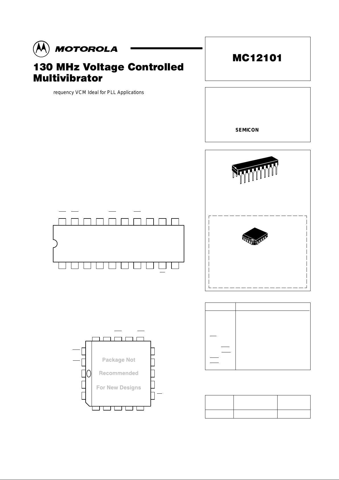
SEMICONDUCTOR
TECHNICAL DATA
130 MHz VOLTAGE
CONTROLLED
MULTIVIBRATOR
Order this document by MC12101/D
Device
Operating
Temperature Range
Package
ORDERING INFORMATION
MC12101P TA = –40° to +75°C Plastic
FN SUFFIX
PLASTIC PACKAGE
CASE 775
(PLCC)
P SUFFIX
PLASTIC PACKAGE
CASE 738
20
1
3
19
4
8
PIN NAMES
Pin Function
RF, RS
V
C
C
B
FS
OE
FST
FSE, FSE
FOE, FOE
EBE
EBT
Center Frequency Inputs
Frequency Control Input
Bias Filter Input
Frequency Select Input
TTL Output Enable
TTL ÷2, ÷4, ÷8 Output
Diff ECL ÷2, ÷4, ÷8 Outputs
Diff ECL ÷1 Outputs
VCO Disable, ECL Level Input
VCO Disable, TTL Level Input
Not Recommended For New Designs
• High Frequency VCM Ideal for PLL Applications
• Single External Resistor Determines Center Frequency; Additional
Resistor Determines f/V Sensitivity
• Internal Ripple Counter (1/2, 1/4, 1/8) for Low Frequency Applications,
TTL/ECL Outputs
• VCO Output Enable Pins (TTL/ECL Level)
• +5.0 V Single Supply Voltage
• Packages: DIP, PLCC
1920 18 17 16 15 14
21 34567
EBT
13
8
12
9
11
10
EBE
V
CC2
FOE FOE FSE FSE V
CC3
FST V
EE3
V
CC1
NC RF RS VCCBV
EE1
FS OE
V
EE2
Pinout: 20-Lead Plastic Package (Top View)
Pinout: 20-Lead PLCC Package (Top View)
EBE
EBT
V
CC
NC
RF
V
CC2
FOE FOE FSE FSE
V
CC3
FST
V
EE3
V
EE2
OE
RS VCCBV
EE1
FS
19
181317 16 15 14
12
11
10
9
45678
20
1
2
3
Motorola, Inc. 1997 Rev 1
Page 2
MC12101
2
MOTOROLA RF/IF DEVICE DATA
EBE
H
L or OPEN
H
EBT
H or OPEN
H
+L
FOE, FSE, FSTLFOE
, FSE
H
OSCILLATION
OSCILLATION
V
CC
Figure 1. Block Diagram
10 11 7 1 13 18
RS 4
RF 3
1
R
X
R
Y
C
F
CENTER
FREQUENCY
SET
VCO
RIPPLE
COUNTER
17 16 15 14
FOE FOE FSE FSE
3:1
MULTIPLEXER
10K
10K
FS
8
OE
9
12
FST
(ECL) (TTL)
20 19
EBT
(TTL)
EBE
(ECL)
7
BIAS FILTER
65
FREQUENCY
CONTROL
INPUT
C
B
C
B
V
C
FS
Level
Divide
Ratio
H
OPEN
L
1/2
1/4
1/8
FREQUENCY SELECT
FUNCTION TABLE
VCO DISABLE FUNCTION TABLE
ABSOLUTE MAXIMUM RATINGS
Parameter Symbol Value Unit
Power Supply Voltage V
CC1
V
CC2
V
CC3
–0.5 to 8.0 V
Input Voltage VIN (TTL) –0.5 to V
CC
V
Input Voltage VIN (ECL) –0.5 to V
CC
V
Output Source Current – Surge
100 mA
Output Source Current – Continuous
I
OUT
(ECL)
50 mA
Junction Operating Temperature T
J
140 °C
Storage Temperature T
STG
–55 to 150 °C
NOTE: ESD data available upon request.
OPERATING CONDITIONS
Parameter Symbol Value Unit
Ambient Temperature T
A
0 to 75 °C
Supply Voltage V
CC
4.75 to 5.25 V
TTL High Output Current IOH (TTL) –1.0 mA
TTL Low Output Current IOL (TTL) 20 mA
Page 3
MC12101
3
MOTOROLA RF/IF DEVICE DATA
DC CHARACTERISTICS (V
CC
= 5.0 V ±5%; RX = 2.4 kΩ; RY = 1.5 kΩ; CB = 0.001 µF, unless otherwise noted.)
0°C 25°C 75°C
Characteristic Symbol Min Max Min Typ Max Min Max Unit Condition
Supply Current I
CC
80 135 70 100 120 85 150 mA EBT = EBE = V
CC
(ECL, TTL)
Output Low Voltage, TTL V
OLT
– – – – 0.5 – – V FS = GND
Output High Voltage, TTL V
OHT
– – 2.4 – – – V FS = GND
Output Low Voltage, ECL V
OLE
– – 3.0 – 3.4 – – V VCC = 5.0 V, RL = 50 Ω,
VT = 3.0 V
Output High Voltage, ECL V
OHE
– – 3.9 – 4.19 – – V VCC = 5.0 V, RL = 50 Ω,
VT = 3.0 V
EBT Input Low Current I
ILT
– – – – 400 – – µA VIN = 0.4 V
EBT Input High Current I
IHT
– – – – 20 – – µA VIN = 2.7 V
– – – – 100 – – µA VIN = 7.0 V
EBE Input High Current I
INHE
– – – – 250 – – µA VIN = 4.19 V
EBE Input Low Current I
INLE
– – 1.0 – – – – µA VIN = 3.05 V
FS Input, Max “L” Level V
ILS
– – – – 1.2 – – V VCC = 5.0 V
FS Input, “Medium” Level V
IMS
– – 2.0 – 3.0 – – V VCC = 5.0 V
FS Input, Min “H” Level V
IHS
– – 3.8 – – – – V VCC = 5.0 V
EBT Input Low Voltage V
ILT
– 0.8 – – 0.8 – 0.8 V
EBT Input High Voltage V
IHT
2.0 – 2.0 – – 2.0 – V
EBE Input High Voltage V
IHE
– – 3.87 – 4.19 – – V VCC = 5.0 V
EBE Input Low Voltage V
ILE
– – 3.05 – 3.52 – – V VCC = 5.0 V
VC Input Voltage,
VC = VCC ÷ 2
V
LM
– – ±1.1 ±1.3 ±1.5 – – V VCC = 5.0 V
CB Output Voltage V
CB
– – 2.35 2.50 2.65 – – V VCC = 5.0 V
AC CHARACTERISTICS (V
CC
= 5.0 V; RX = 2.4 kΩ; RY = 1.5 kΩ; CB = 0.001 µF; VT = 3.0 V, unless otherwise noted.)
0°C 25°C 75°C
Characteristic Symbol Min Max Min Typ Max Min Max Unit Condition
Center Frequency (VVC – VCB = 0V) FO – – 117 130 143 – – MHz VCC = 2.0 V
VEE = –3.0 V
Frequency Range
(VC = 1/2 VCC ±1.5V, VCC = 5.0V)
F
MAX
–
F
MIN
– – 68 80 92 – – MHz
FOE/FOE/FSE/FSE Rise Time t
rE
– – 0.5 – 2.4 – – ns
FOE/FOE/FSE/FSE Fall Time t
fE
– – 0.5 – 2.4 – – ns
Reset Time TTT – – – – 40 – – ns EBTXFST
Reset Time TTO – – – – 25 – – ns EBTXFOE/FOE
Reset Time TTS – – – – 35 – – ns EBTXFSE/FSE
Reset Time TET – – – – 32 – – ns EBEXFST
Reset Time TEO – – – – 12 – – ns EBEXFOE/FOE
Reset Time TES – – – – 30 – – ns EBEXFSE/FSE
NOTE: Loading: ECL = 50 Ω to VT; TTL = 500 Ω, 50 pF
Page 4

MC12101
4
MOTOROLA RF/IF DEVICE DATA
OUTPUT FREQUENCY FORMULA
1) CENTER FREQUENCY : f
OSC
]
560
R
X
)
1.0
(MHz)
RX in k
Ω
Units: 2.7 kΩ ≤ RX ≤ 3.6 k
Ω
2) GAIN : Af]
320
V
CC
@
R
Y
(MHzńV)
RY in k
Ω
Units: 1.5 kΩ ≤ RY ≤ 2.4 k
Ω
Figure 2. VCO Detail
1/2
V
CC
V
CB
–
+
±0.75V
Limit
40K
40K
–
+
R
Y
R
X
34561
C
B
V
CC1
C
F
V
CC1
V
C
CB = 0.001µF
CF = 0.1
µ
F
Notes:
• For optimum VCO linearity (MHz/V), the following resistor ranges are recommended:
3.6 kΩ ≤ RX ≤ 4.6 kΩ (RY = 2.0 kΩ)
1.5 kΩ ≤ RY ≤ 2.4 kΩ (RX = 3.3 kΩ)
• TTL output maximum frequency = 50 MHz
• Simultaneous use of both ECL and TTL outputs are not recommended due to excessive power consumption for the EIAJ
Type II SO package
Figure 3. AC Test Circuit (FO/trE/tfE Measurement) Figure 4. AC Test Circuit (Other Measurements)
R
X
R
Y
3
4
5
19
20
6
7 10 11
VEE = GND
0.1
µ
F
1 18 13
VCC = +5.0VDC
0.1µF
0.1µF
16
17
50
Ω
50
Ω
+3.0V
14
15
50
Ω
50
Ω
+3.0V
12
50pF
500
Ω
R
X
R
Y
9
3
4
5
6
7 10 11
VEE = –3.0VDC
0.1
µ
F
1 18 13
VCC = +2.0VDC
0.1µF
0.1µF
16
17
14
15
V
IE
V
IT
0.001µF
Page 5

MC12101
5
MOTOROLA RF/IF DEVICE DATA
Figure 5. Switching Waveforms
TTT
TTS
TTO
TES
TET
EBT
EBE
FOE
FSE
FST
50%
50%
50%
50%
50%
TEO
EBE
H
L or OPEN
H
EBT
H or OPEN
H
L
FOE, FSE, FSTLFOE
, FSE
H
OSCILLATION
OSCILLATION
VCO DISABLE FUNCTION TABLE
Page 6

MC12101
6
MOTOROLA RF/IF DEVICE DATA
200
150
100
50
0
1.0 1.5 2.0 2.5 3.0 3.5 4.0
FREQUENCY (MHz)
VC (VOLTS)
Rx = 3.0 k
Rx = 3.3 k
Rx = 3.6 k
Ry = 1.5 k
Ry = 2.0 k
Ry = 2.4 k
0°C
25°C
75°C 5.25 V
5.00 V
4.75 V
200
150
100
50
0
1.0 1.5 2.0 2.5 3.0 3.5 4.0
FREQUENCY (MHz)
VC (VOLTS)
200
150
100
50
0
1.0 1.5 2.0 2.5 3.0 3.5 4.0
FREQUENCY (MHz)
VC (VOLTS)
200
150
100
50
0
1.0 1.5 2.0 2.5 3.0 3.5 4.0
FREQUENCY (MHz)
VC (VOLTS)
Figure 6. VC versus Output Frequency
(Varying Rx @ VCC = 5.0 V; TA = 25°C; Ry = 2.0 kΩ)
Figure 7. VC versus Output Frequency
(Varying Ry @ VCC = 5.0 V; TA = 25°C; Ry = 3.3 kΩ)
Figure 8. VC versus Output Frequency
(Varying TA @ VCC = 5.0 V; Rx = 3.3 kΩ; Ry = 2.0 kΩ )
Figure 9. VC versus Output Frequency
(Varying VCC @ Rx = 3.3 kΩ; Ry = 2.0 kΩ; TA = 25°C)
Page 7

MC12101
7
MOTOROLA RF/IF DEVICE DATA
P SUFFIX
PLASTIC PACKAGE
CASE 738–03
ISSUE E
1.070
0.260
0.180
0.022
0.070
0.015
0.140
15°
0.040
1.010
0.240
0.150
0.015
0.050
0.008
0.110
0
°
0.020
25.66
6.10
3.81
0.39
1.27
0.21
2.80
0
°
0.51
27.17
6.60
4.57
0.55
1.77
0.38
3.55
15
°
1.01
0.050 BSC
0.100 BSC
0.300 BSC
1.27 BSC
2.54 BSC
7.62 BSC
MIN MINMAX MAX
INCHES MILLIMETERS
DIM
A
B
C
D
E
F
G
J
K
L
M
N
NOTES:
1. DIMENSIONING AND TOLERANCING PER ANSI
Y14.5M, 1982.
2. CONTROLLING DIMENSION: INCH.
3. DIMENSION L TO CENTER OF LEAD WHEN
FORMED PARALLEL.
4. DIMENSION B DOES NOT INCLUDE MOLD
FLASH.
-A-
C
K
N
E
GF
D
20 PL
J 20 PL
L
M
-T-
SEATING
PLANE
110
1120
0.25 (0.010) T A
M M
0.25 (0.010) T B
M M
B
OUTLINE DIMENSIONS
Motorola reserves the right to make changes without further notice to any products herein. Motorola makes no warranty , representation or guarantee regarding
the suitability of its products for any particular purpose, nor does Motorola assume any liability arising out of the application or use of any product or circuit, and
specifically disclaims any and all liability, including without limitation consequential or incidental damages. “T ypical” parameters which may be provided in Motorola
data sheets and/or specifications can and do vary in different applications and actual performance may vary over time. All operating parameters, including “Typicals”
must be validated for each customer application by customer’s technical experts. Motorola does not convey any license under its patent rights nor the rights of
others. Motorola products are not designed, intended, or authorized for use as components in systems intended for surgical implant into the body, or other
applications intended to support or sustain life, or for any other application in which the failure of the Motorola product could create a situation where personal injury
or death may occur. Should Buyer purchase or use Motorola products for any such unintended or unauthorized application, Buyer shall indemnify and hold Motorola
and its officers, employees, subsidiaries, affiliates, and distributors harmless against all claims, costs, damages, and expenses, and reasonable attorney fees
arising out of, directly or indirectly, any claim of personal injury or death associated with such unintended or unauthorized use, even if such claim alleges that
Motorola was negligent regarding the design or manufacture of the part. Motorola and are registered trademarks of Motorola, Inc. Motorola, Inc. is an Equal
Opportunity/Affirmative Action Employer.
Mfax is a trademark of Motorola, Inc.
How to reach us:
USA/EUROPE/Locations Not Listed: Motorola Literature Distribution; JAPAN: Nippon Motorola Ltd.: SPD, Strategic Planning Office, 141,
P.O. Box 5405, Denver, Colorado 80217. 1–303–675–2140 or 1–800–441–2447 4–32–1 Nishi–Gotanda, Shagawa–ku, Tokyo, Japan. 03–5487–8488
Customer Focus Center: 1–800–521–6274
Mfax: RMFAX0@email.sps.mot.com – TOUCHTONE 1–602–244–6609 ASIA/PACIFIC: Motorola Semiconductors H.K. Ltd.; 8B Tai Ping Industrial Park,
Moto rola Fax Back System – US & Canada ONLY 1–800–774–1848 51 Ting Kok Road, Tai Po, N.T., Hong Kong. 852–26629298
– http://sps.motorola.com/mfax/
HOME PAGE: http://motorola.com/sps/
MC12101/D
◊
 Loading...