

Page 1
SEMICONDUCTOR
TECHNICAL DATA
MECL PLL COMPONENTS
÷8192 PRESCALER
Order this document by MC12098/D
Device
Operating
Temperature Range
Package
ORDERING INFORMATION
MC12098D TA = –40° to +85°C SO–8
PIN CONNECTIONS
D SUFFIX
PLASTIC PACKAGE
CASE 751
(SO–8)
1
8
NC
(Top View)
8
Gnd
IN
IN
V
CC
OUT
V
CCO
GndO
7
6
5
1
2
3
4
The MC12098 is a single modulus divide by 8192 prescaler for low power
frequency division of a 2.5 GHz high frequency input signal. The low power
(3.6 mA typical at 5.0 V) and high operating frequency features make this
prescaler ideal in satellite TV receiver applications.
The MC12098 is pin and functionally compatible to the Plessey SP4982,
but with significantly lower power consumption.
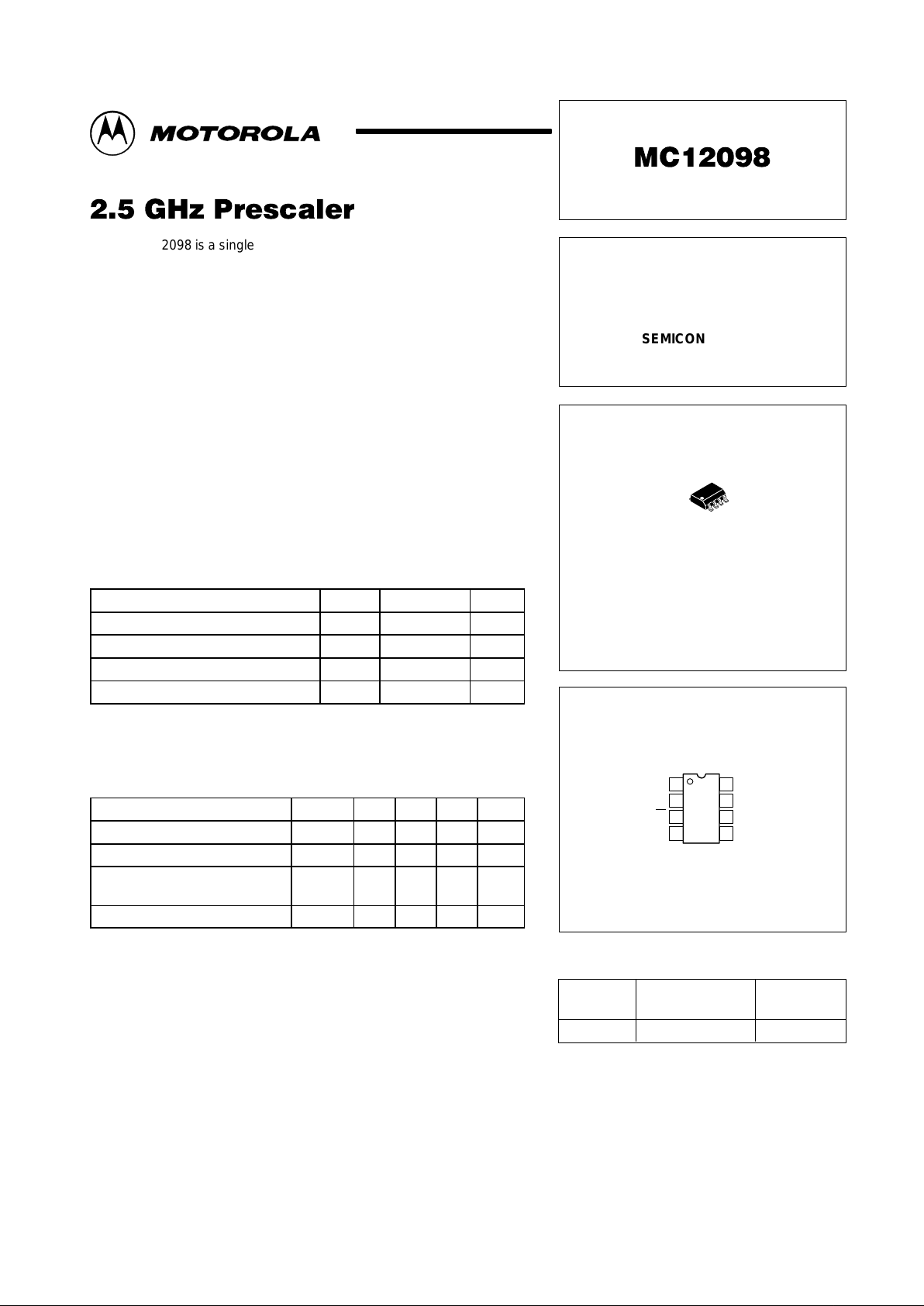
On-chip output termination provides 2.0 mA of output current to drive a
12 pF (typical) high impedance load. The output voltage swing under typical
supply voltage and temperature conditions is 1.1 V. If additional drive is
required for the prescaler output, an external resistor can be added in
parallel from the OUT pin to GND to increase the output power . Care must be
taken not to exceed the maximum allowable current through the output.
• 2.5 GHz Toggle Frequency
• Supply Voltage 2.7 to 5.5 V
• Low Power Dissipation 18 mW Typical
• Operating Temperature Range of –40 to 85°C
MAXIMUM RATINGS
Parameter Symbol Value Unit
Power Supply Voltage, Pin 4 V
CC
–0.5 to 6.0 VDC
Operating Temperature Range T
A
–40 to 85 °C
Storage Temperature Range Tstg –65 to 150 °C
Maximum Output Current, Pin 7 I
O
4.0 mA
NOTE: ESD data available upon request.
ELECTRICAL CHARACTERISTICS (V
CC
= 2.7 to 5.5 V; TA = –40 to 85°C,
unless otherwise noted.)
Parameter
Symbol Min Typ Max Unit
Toggle Frequency (Sine Wave) ft 0.5 3.0 2.5 GHz
Supply Current Output (Pin 4) I
CC
- 3.6 6.5 mA
Input Voltage Sensitivity
500–2500 MHz
V
in
140 - 1000
mVpp
Output Voltage Swing (Note 1) V
out
0.8 1.1 - V
pp
NOTE: 1.Assumes CL = 12 pF
Motorola, Inc. 1997 Rev 2
Page 2
MC12098
2
MOTOROLA RF/IF DEVICE DATA
Figure 1. MC12098 Block Diagram
÷
8192
V
CCO
OUT
11 k
Ω
V
REF
IN
IN
GND
5000
Ω
5000
Ω
V
REF
≈ 2.0 V @ VCC = 3.0 V
V
REF
≈
3.5 V @ VCC = 5.0 V
V
CC
GNDO
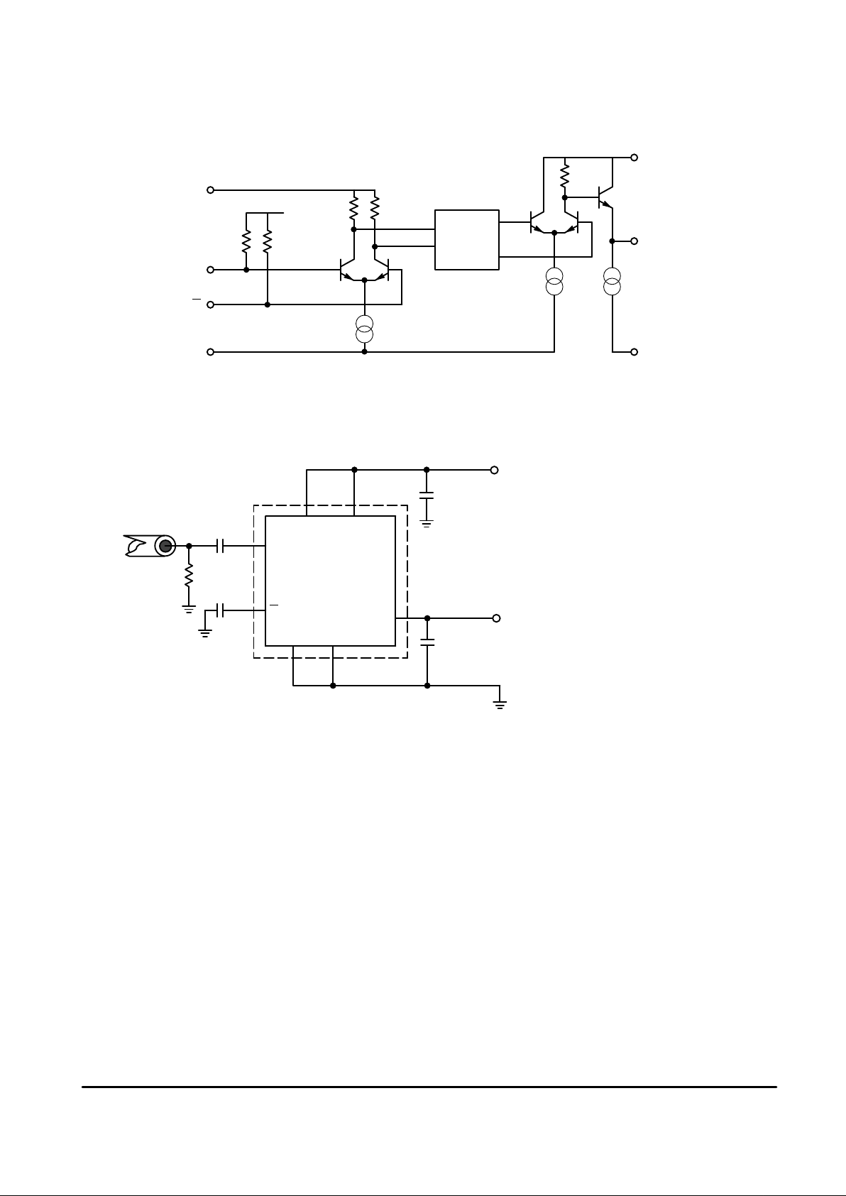
Figure 2. AC Test Circuit
SINE WAVE GENERATOR
50
Ω
C1
C2
C3
VCC = 2.7 to 5.5 V
C
L
V
CC
IN
IN
GND
OUT
EXTERNAL COMPONENTS
C1 = C2 = 1000 pF
C3 = 0.1
µ
F
CL = 12 pF (Including Scope and Jig Capacitance)
GNDO
V
CCO
Page 3

MC12098
3
MOTOROLA RF/IF DEVICE DATA
Figure 3. MC12098 Input Signal Amplitude versus Input Frequency
(VCC = 5.5 V , TA = 25°C)
Page 4

MC12098
4
MOTOROLA RF/IF DEVICE DATA
–450
–400
–350
–300
–250
–200
–150
–100
–50
0
50
300 500 700 900 1100 1300 1500 1700 1900 2100 2300 2500 2700
Figure 4. Input Impedance versus Frequency
5
15
25
35
45
55
300 500 700 900 1100 1300 1500 1700 1900 2100 2300 2500 2700
Input Frequency (MHz)
R (Ohms)
Figure 5. Input Impedance versus Frequency
Input Frequency (MHz)
jX (Ohms)
Page 5

MC12098
5
MOTOROLA RF/IF DEVICE DATA
D SUFFIX
PLASTIC PACKAGE
CASE 751–06
(SO–8)
ISSUE T
SEATING
PLANE
1
4
58
A0.25MCB
SS
0.25MB
M
h
q
C
X 45
_
L
DIM MIN MAX
MILLIMETERS
A 1.35 1.75
A1 0.10 0.25
B 0.35 0.49
C 0.19 0.25
D 4.80 5.00
E
1.27 BSCe
3.80 4.00
H 5.80 6.20
h
0 7
L 0.40 1.25
q
0.25 0.50
__
NOTES:
1. DIMENSIONING AND TOLERANCING PER ASME
Y14.5M, 1994.
2. DIMENSIONS ARE IN MILLIMETER.
3. DIMENSION D AND E DO NOT INCLUDE MOLD
PROTRUSION.
4. MAXIMUM MOLD PROTRUSION 0.15 PER SIDE.
5. DIMENSION B DOES NOT INCLUDE DAMBAR
PROTRUSION. ALLOWABLE DAMBAR
PROTRUSION SHALL BE 0.127 TOTAL IN EXCESS
OF THE B DIMENSION AT MAXIMUM MATERIAL
CONDITION.
D
E
H
A
B
e
B
A1
C
A
0.10
OUTLINE DIMENSIONS
Motorola reserves the right to make changes without further notice to any products herein. Motorola makes no warranty , representation or guarantee regarding
the suitability of its products for any particular purpose, nor does Motorola assume any liability arising out of the application or use of any product or circuit, and
specifically disclaims any and all liability, including without limitation consequential or incidental damages. “T ypical” parameters which may be provided in Motorola
data sheets and/or specifications can and do vary in different applications and actual performance may vary over time. All operating parameters, including “Typicals”
must be validated for each customer application by customer’s technical experts. Motorola does not convey any license under its patent rights nor the rights of
others. Motorola products are not designed, intended, or authorized for use as components in systems intended for surgical implant into the body, or other
applications intended to support or sustain life, or for any other application in which the failure of the Motorola product could create a situation where personal injury
or death may occur. Should Buyer purchase or use Motorola products for any such unintended or unauthorized application, Buyer shall indemnify and hold Motorola
and its officers, employees, subsidiaries, affiliates, and distributors harmless against all claims, costs, damages, and expenses, and reasonable attorney fees
arising out of, directly or indirectly, any claim of personal injury or death associated with such unintended or unauthorized use, even if such claim alleges that
Motorola was negligent regarding the design or manufacture of the part. Motorola and are registered trademarks of Motorola, Inc. Motorola, Inc. is an Equal
Opportunity/Affirmative Action Employer.
Mfax is a trademark of Motorola, Inc.
How to reach us:
USA/EUROPE/ Locations Not Listed: Motorola Literature Distribution; JAPAN: Nippon Motorola Ltd.: SPD, Strategic Planning Office, 141,
P.O. Box 5405, Denver, Colorado 80217. 1–303–675–2140 or 1–800–441–2447 4–32–1 Nishi–Gotanda, Shagawa–ku, T o kyo, Japan. 03–5487–8488
Customer Focus Center: 1–800–521–6274
Mfax: RMFAX0@email.sps.mot.com – TOUCHTONE 1–602–244–6609 ASIA/PACIFIC: Motorola Semiconductors H.K. Ltd.; 8B Ta i Ping Industrial Park,
Moto rola Fax Back System – US & Canada ONLY 1–800–774–1848 51 Ting Kok Road, Tai Po, N.T., Hong Kong. 852–26629298
– http://sps.motorola.com/mfax/
HOME PAGE: http://motorola.com/sps/
MC12098/D
◊
 Loading...