

Page 1
查询MC12053AD供应商
$ ! " "
! !!
#
The MC12053A is a super low power ÷64/65, ÷128/129 dual modulus
prescaler. Motorola’ s advanced Bipolar MOSAIC V technology is utilized to
achieve low power dissipation of 4.3 mW at a minimum supply voltage of
2.7 V.
The Divide Ratio Control input, SW, permits selection of divide ratio as
desired. A HIGH on SW selects
The Modulus Control input, MC, selects the proper divide number after SW
has been biased to select the desired divide ratio.
Stand–by mode is featured to reduce current drain to 50 µA typical at
2.7 V when the stand–by pin, SB, is switched LOW, disabling the prescaler.
On–chip output termination provides 500 µA (typical) output current, which is
sufficient to drive a CMOS synthesizer input high impedance load (8.0 pF
typical).
• 1.1 GHz Toggle Frequency
• Supply Voltage of 2.7 to 5.5 V
• Low Power 1.5 mA Typical at V
• Operating Temperature Range of –40 to 85°C
• On–Chip Output Termination
• The MC12053A Is Pin and Functionally Compatible With the MC12036
• Modulus Control Input Level Is Compatible With Standard CMOS and
TTL
MOSAIC V is a trademark of Motorola
FUNCTIONAL TABLE
SW MC Divide Ratio
H H 64
H L 65
L H 128
L L 129
NOTES: 1.SW: H = VCC – 0.5 to VCC, L = Open. A logic L can also be applied by grounding
this pin, but this is not recommended due to increased power consumption.
2.MC & SB: H = 2.0 V to VCC, L = Gnd to 0.8 V.
MAXIMUM RATINGS
Characteristic Symbol Range Unit
Power Supply Voltage, Pin 2 V
Operating Temperature Range T
Storage Temperature Range T
Modulus Control Input, Pin 6 MC –0.5 to V
Maximum Output Current, Pin 4 I
NOTE: ESD data available upon request.
÷64/65; an OPEN on SW selects ÷128/129.
= 2.7 V
CC
CC
A
stg
O
–0.5 to 7.0 Vdc
–40 to 85 °C
–65 to 150 °C
CC
4.0 mA
Vdc
Order this document by MC12053A/D
MECL PLL COMPONENTS
÷64/65, ÷128/129 LOW POWER
DUAL MODULUS PRESCALER
WITH STAND–BY MODE
SEMICONDUCTOR
TECHNICAL DATA
8
1
D SUFFIX
PLASTIC PACKAGE
CASE 751
(SO–8)
8
1
SD SUFFIX
PLASTIC PACKAGE
CASE 940
(SSOP–8)
PIN CONNECTIONS
(Top View)
TA =
8
IN
7
SB
6
MC
5
Gnd
Package
SO–8
SSOP–8
ORDERING INFORMATION
Device
MC12053AD
MC12053ASD
1
IN
2
V
CC
3
SW
4
OUT
Operating
Temp Range
–40° to +85°C
Motorola, Inc. 1997 Rev 4
Page 2
MC12053A
ELECTRICAL CHARACTERISTICS (VCC = 2.7 to 5.5 V; TA = –40 to 85°C, unless otherwise notex.)
Characteristic Symbol Min Typ Max Unit
Toggle Frequency (Sine Wave Input) f
Supply Current Output (Pin 2) VCC = 2.7 V
VCC = 5.0 V
Stand–By Current VCC = 2.7 V
VCC = 5.0 V
Modulus Control & Stand–By Input HIGH (MC & SB) V
Modulus Control & Stand–By Input LOW (MC & SB) V
Divide Ratio Control Input HIGH (SW) V
Divide Ratio Control Input LOW (SW) V
Output Voltage Swing (Note 1) V
Modulus Setup Time MC to OUT at 1100 MHz t
Input Voltage Sensitivity 250–1 100 MHz
100–250 MHz
NOTE: Assumes 8.0 pF high impedance load.
I
I
V
t
CC
SB
IH1
IL1
IH2
IH2
out
set
in
0.1 1.4 1.1 GHz
–
–
–
–
1.60
1.75
50
100
2.0 – VCC + 0.5 V
Gnd – 0.8 V
VCC – 0.5 V
CC
Open Open Open
0.8 1.1 – V
– 11 16 ns
100
400
–
–
2.5
mA
2.5
250
250
VCC + 0.5 V
1000
mVpp
1000
µA
pp
In
In
MC
SB
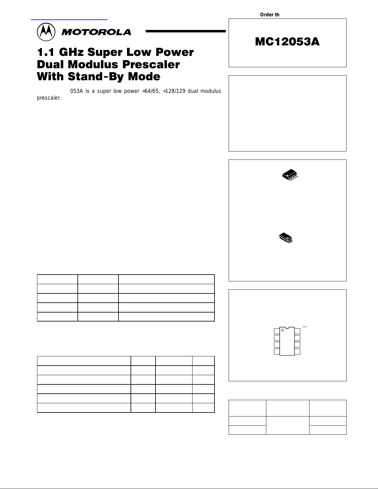
Figure 1. Logic Diagram (MC12053A)
QD
A
QBC
QD
QBC
QBD
Q
C
QD
B
QBC
QD
QBC
C
QB
C
M
QBD
QC
SW
Sine Wave Generator
C1
IN
50
Ω
C2
IN
QD
QBD
HGFED
Q
C
S
Figure 3. AC Test Circuit
CC
SWV
SB
OUT
MC
GND
Out
C3
Figure 2. Modulus Setup Time
Prop. Delay
MC Setup
MC Release
Modulus setup time MC to out is the MC
setup or MC release plus the prop delay.
VCC = 2.7 to 5.5 V
C
EXTERNAL COMPONENTS
L
C1 = C2 = 1000 pF
µ
C3 = 0.1
F
CL = 8.0 pF (Including Scope
and jig capacitance)
In
Out
MC
MC Input
2
MOTOROLA RF/IF DEVICE DATA
Page 3
MC12053A
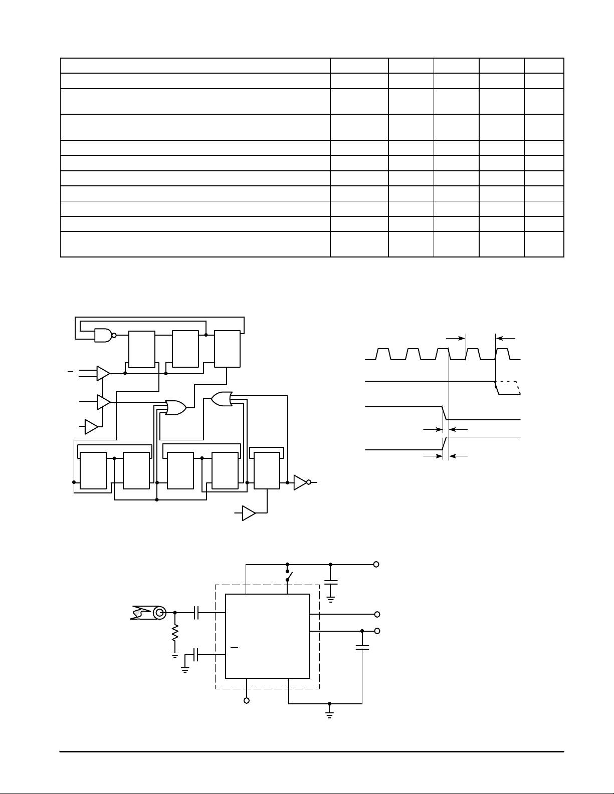
Figure 4. Input Signal Amplitude versus Input Frequency
+15.0
+10.0
+5.0
0
–5.0
–10.0
–15.0
–20.0
–25.0
AMPLITUDE (dBm)
–30.0
–35.0
–40.0
–45.0
–50.0
0 200 400 600 800 1000 1200 1400 1600 1800
OPERATING
WINDOW
FREQUENCY (MHz)
Divide Ratio = 64; VCC = 2.7 V; TA = 25°C
+1257.40
+707.11
+397.64
+223.61
+125.74
+70.71
+39.76
+22.36
+12.57
+7.07
+3.98
+2.24
+1.26
+0.71
mVrms
Figure 5. Output Amplitude versus Input Frequency
2000
1600
1200
800
400
0
0
200 400 600 800 1000 1200 1400 1600 1800
FREQUENCY (MHz)
mVpp
MOTOROLA RF/IF DEVICE DATA
3
Page 4

R
OHMS
MC12053A
Figure 6. T ypical Input Impedance versus Input Frequency
300
200
100
0
–100
–200
–300
–400
–500
–600
–700
MHz
–800
jX
–900
–1000
–1100
–1200
100 200 300 400 500 600 700 800 900 1000 1100 1200
4
MOTOROLA RF/IF DEVICE DATA
Page 5

C
A
E
B
A1
MC12053A
OUTLINE DIMENSIONS
D SUFFIX
PLASTIC PACKAGE
CASE 751–06
(SO–8)
M
h
ISSUE T
X 45
_
C
q
D
58
0.25MB
1
H
4
e
A
SEATING
PLANE
0.10
L
B
SS
A0.25MCB
SD SUFFIX
PLASTIC PACKAGE
CASE 940–03
(SSOP–8)
ISSUE B
NOTES:
1. DIMENSIONING AND TOLERANCING PER ASME
Y14.5M, 1994.
2. DIMENSIONS ARE IN MILLIMETER.
3. DIMENSION D AND E DO NOT INCLUDE MOLD
PROTRUSION.
4. MAXIMUM MOLD PROTRUSION 0.15 PER SIDE.
5. DIMENSION B DOES NOT INCLUDE DAMBAR
PROTRUSION. ALLOWABLE DAMBAR
PROTRUSION SHALL BE 0.127 TOTAL IN EXCESS
OF THE B DIMENSION AT MAXIMUM MATERIAL
CONDITION.
MILLIMETERS
DIM MIN MAX
A 1.35 1.75
A1 0.10 0.25
B 0.35 0.49
C 0.19 0.25
D 4.80 5.00
E
3.80 4.00
1.27 BSCe
H 5.80 6.20
h
0.25 0.50
L 0.40 1.25
0 7
q
__
L/2
L
PIN 1
IDENT
0.20 (0.008) T
0.076 (0.003)
SEATING
–T–
PLANE
K8X REF
0.12 (0.005) V
85
41
A
–V–
M
U
C
D
G
M
S
U
T
S
N
0.25 (0.010)
M
N
B
F
DETAIL E
K
–U–
J
S
K1
J1
SECTION N–N
–W–
DETAIL E
H
NOTES:
1 DIMENSIONING AND TOLERANCING PER ANSI
Y14.5M, 1982.
2 CONTROLLING DIMENSION: MILLIMETER.
3 DIMENSION A DOES NOT INCLUDE MOLD FLASH,
PROTRUSIONS OR GATE BURRS. MOLD FLASH
OR GATE BURRS SHALL NOT EXCEED 0.15
(0.006) PER SIDE.
4 DIMENSION B DOES NOT INCLUDE INTERLEAD
FLASH OR PROTRUSION. INTERLEAD FLASH OR
PROTRUSION SHALL NOT EXCEED 0.15 (0.006)
PER SIDE.
5 DIMENSION K DOES NOT INCLUDE DAMBAR
PROTRUSION/INTRUSION. ALLOWABLE DAMBAR
PROTRUSION SHALL BE 0.13 (0.005) TOTAL IN
EXCESS OF K DIMENSION AT MAXIMUM
MATERIAL CONDITION. DAMBAR INTRUSION
SHALL NOT REDUCE DIMENSION K BY MORE
THAN 0.07 (0.002) AT LEAST MATERIAL
CONDITION.
6 TERMINAL NUMBERS ARE SHOWN FOR
REFERENCE ONLY.
7 DIMENSION A AND B ARE TO BE DETERMINED
AT DATUM PLANE –W–.
MILLIMETERS
DIMAMIN MAX MIN MAX
2.87 3.13 0.113 0.123
B 5.20 5.38 0.205 0.212
C 1.73 1.99 0.068 0.078
D 0.05 0.21 0.002 0.008
F 0.63 0.95 0.024 0.037
G 0.65 BSC 0.026 BSC
H 0.44 0.60 0.017 0.023
J 0.09 0.20 0.003 0.008
J1 0.09 0.16 0.003 0.006
K 0.25 0.38 0.010 0.015
K1 0.25 0.33 0.010 0.013
L 7.65 7.90 0.301 0.311
M 0 8 0 8
____
INCHES
MOTOROLA RF/IF DEVICE DATA
5
Page 6

MC12053A
Motorola reserves the right to make changes without further notice to any products herein. Motorola makes no warranty , representation or guarantee regarding
the suitability of its products for any particular purpose, nor does Motorola assume any liability arising out of the application or use of any product or circuit, and
specifically disclaims any and all liability, including without limitation consequential or incidental damages. “T ypical” parameters which may be provided in Motorola
data sheets and/or specifications can and do vary in different applications and actual performance may vary over time. All operating parameters, including “Typicals”
must be validated for each customer application by customer’s technical experts. Motorola does not convey any license under its patent rights nor the rights of
others. Motorola products are not designed, intended, or authorized for use as components in systems intended for surgical implant into the body, or other
applications intended to support or sustain life, or for any other application in which the failure of the Motorola product could create a situation where personal injury
or death may occur. Should Buyer purchase or use Motorola products for any such unintended or unauthorized application, Buyer shall indemnify and hold Motorola
and its officers, employees, subsidiaries, affiliates, and distributors harmless against all claims, costs, damages, and expenses, and reasonable attorney fees
arising out of, directly or indirectly, any claim of personal injury or death associated with such unintended or unauthorized use, even if such claim alleges that
Motorola was negligent regarding the design or manufacture of the part. Motorola and are registered trademarks of Motorola, Inc. Motorola, Inc. is an Equal
Opportunity/Affirmative Action Employer.
6
MOTOROLA RF/IF DEVICE DATA
Page 7

MC12053A
How to reach us:
USA/EUROPE/Locations Not Listed: Motorola Literature Distribution; JAPAN: Nippon Motorola Ltd.: SPD, Strategic Planning Office, 141,
P.O. Box 5405, Denver, Colorado 80217. 1–303–675–2140 or 1–800–441–2447 4–32–1 Nishi–Gotanda, Shagawa–ku, Tokyo, Japan. 03–5487–8488
Customer Focus Center: 1–800–521–6274
Mfax: RMFAX0@email.sps.mot.com – TOUCHTONE 1–602–244–6609 ASIA/PACIFIC: Motorola Semiconductors H.K. Ltd.; 8B Tai Ping Industrial Park,
Moto rola Fax Back Sys tem – US & Canada ONLY 1–800–774–1848 51 Ting Kok Road, Tai Po, N.T ., Hong Kong. 852–26629298
HOME PAGE: http://motorola.com/sps/
MOTOROLA RF/IF DEVICE DATA
– http://sps.motorola.com/mfax/
◊
Mfax is a trademark of Motorola, Inc.
MC12053A/D
7
 Loading...