

Page 1
These devices are two–modulus prescalers which will divide by 5 and
6, 8 and 9, and 10 and 11, respectively. A MECL–to–MTTL translator is
provided to interface directly with the MC12014 Counter Control Logic. In
addition, there is a buffered clock input and MECL bias voltage source.
• MC12009 480 MHz (
550 MHz (B10/11)
• MECL to MTTL Translator on Chip
• MECL and MTTL Enable Inputs
• 5.0 or –5.2 V Operation*
• Buffered Clock Input — Series Input RC Typ, 20 Ohms and 4 pF
• V
Reference Voltage
BB
• 310 Milliwatts (Typ)
B
5/6), MC12011 550 MHz (B8/9), MC12013
Order this document by MC12009/D
MECL PLL COMPONENTS
DUAL MODULUS PRESCALER
SEMICONDUCTOR
TECHNICAL DATA
* When using a 5.0 V supply, apply 5.0 V to Pin 1 (V
(MTTL VCC), Pin 16 (VCC), and ground Pin 8 (VEE). When using
–5.2 V supply, ground Pin 1 (V
Pin 16 (VCC) and apply –5.2 V to Pin 8 (VEE). If the translator is not
required, Pin 6 may be left open to conserve dc power drain.
), Pi n 6 (MTT L VCC), and
CCO
CCO
MAXIMUM RATINGS
Characteristic Symbol Rating Unit
(Ratings above which device life may be impaired)
Power Supply Voltage
(VCC = 0)
Input Voltage
(VCC = 0)
Output Source Current
Continuous
Surge
Storage Temperature Range T
(Recommended Maximum Ratings above which performance may be
degraded)
Operating Temperature Range
MC12009, MC12011, MC12013
DC Fan–Out (Note 1)
(Gates and Flip–Flops)
NOTES: 1. AC fan–out is limited by desired system performance.
2.ESD data available upon request.
V
EE
V
in
I
O
stg
T
A
n 70 —
–8.0 Vdc
0 to V
EE
t
50
t
100
–65 to +175 °C
–30 to +85 °C
), Pi n 6
Vdc
mAdc
16
1
P SUFFIX
PLASTIC PACKAGE
CASE 648
PIN CONNECTIONS
116
V
CCO
Q
2
Q
3
( – )
4
5
( + )
MTTL V
MTTL Output
6
CC
7
8
V
EE
(Top View)
ORDERING INFORMATION
Operating
Device
MC12009P
MC12011P TA = – 35° to +85°C
MC12013P
Temperature Range
15
14
13
12
11
10
9
V
CC
Clock
V
BB
E1 MECL
E2 MECL
E3 MECL
E4 MECL
E5 MECL
Package
Plastic
Motorola, Inc. 1997 Rev 2
Page 2
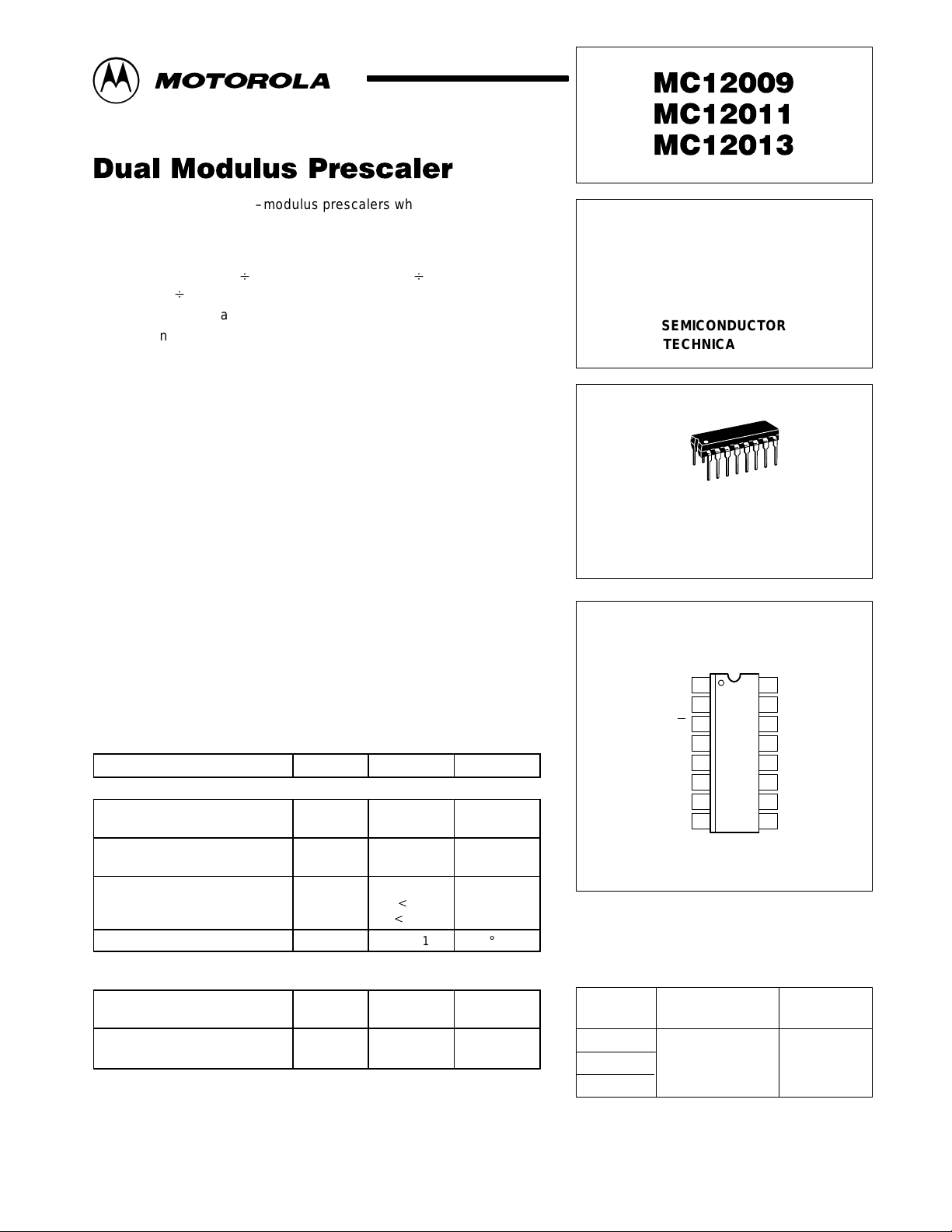
MTTL E5
MTTL E4
MECL E3
MECL E2
MECL E1
MC12009 MC12011 MC12013
Figure 1. Logic Diagrams
MC12009
9
10
11
12
13
15
Q1
DQ2
C
Q
Recommended Circuitry
For ac coupled Inputs.
1000 pF
Clock Input
1
1 k
MC12011
D
C
D
C
0.1 µF
Q3
Q3
V
BB
14
Q
2
3
Q3
3
MECL
to
MTTL
Trans–
lator
45
–+
7
MTTL
Out
MTTL E5 9
10
MTTL E4
11
MECL E3
12
MECL E2
13
MECL E1
÷ 10 for one or all
E1 thru E5 high
÷ 11 for all
E1 thru E5 low
Tie unused gate inputs low .
MTTL E5 9
10
MTTL E4
11
MECL E3
12
MECL E2
13
MECL E1
Pull–down resistors required on
Pins 2, 3 when not connected
to translator.
Basic IC Capability: ÷ 10/11
Q2
DCQ1 Q3
Recommended Circuitry
For ac coupled Inputs.
15
1000 pF
Clock Input
Q1
D
C
Recommended Circuitry
For ac coupled Inputs.
15
1000 pF
1000 pF
Clock Input
Clock Input
D
C
1 k
MC12013
D
C
1 k
Q2
0.1
0.1
D
C
V
BB
14
µ
F
Q3D
C
V
BB
14
µ
F
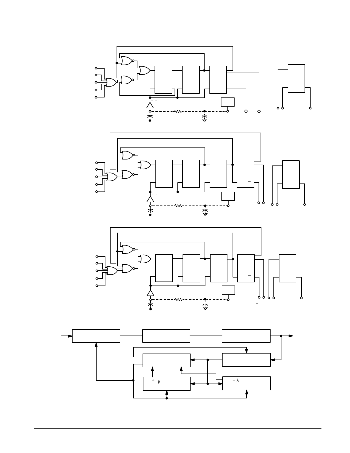
Figure 2. T ypical Frequency Synthesizer Application
T oggle
Flip
Flop
C
Toggle
Flop
C
Flip
Q4
Q
Q4
Q
4
4
32
Q
4Q4
Q4Q4
23
54
+–
45
–+
MECL
to
MTTL
Trans–
lator
7
MTTL
Out
MECL
to
MTTL
Trans–
lator
7
MTTL
Out
f
ref
Phase Detector
MC4044
f
out
Low–Pass Filter
Modulus Enable Line
Counter Control Logic
MC12014
B
Np Programmable
Counter MC4016
Counter Reset Line
Zero Detect Line
2
Voltage–Controlled
Oscillator MC1648
MC12009
MC12011
MC12013
B
A Programmable
Counter MC4016
f
out
MOTOROLA RF/IF DEVICE DATA
Page 3
MC12009 MC12011 MC12013
Under
pp y
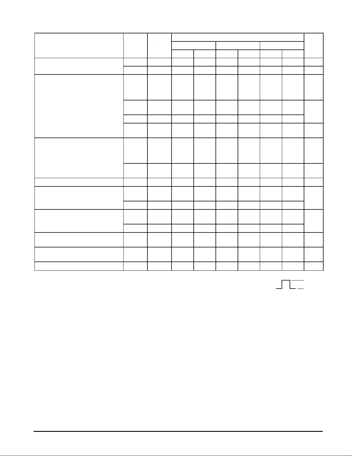
ELECTRICAL CHARACTERISTICS (Supply Voltage = –5.2 V, unless otherwise noted.)
Test Limits
Pin
Characteristic Symbol
Power Supply Drain Current
Input Current I
Leakage Current I
Reference Voltage V
Logic ‘1’ Output Voltage V
Logic ‘0’ Output Voltage V
Logic ‘1’ Threshold Voltage V
Logic ‘0’ Threshold Voltage V
Short Circuit Current I
1. Test outputs of the device must be tested by sequencing through the truth table. All input, power supply and
ground voltages must be maintained between tests. The clock input is the waveform shown.
2. In addition to meeting the output levels specified, the device must divide by 5, 8 or 10 during this test. The clock
input is the waveform shown.
3. In addition to meeting the output levels specified, the device must divide by 6, 9 or 11 during this test. The clock
input is the waveform shown.
I
CC1
I
CC2
inH1
I
inH2
I
inH3
I
inH4
inL1
I
inL2
BB
OH1
(Note 1)
V
OH2
OL1
(Note 1)
V
OL2
OHA
(Note 2)
OLA
(Note 3)
OS
Under
Test
8 –88 –80 –80 mAdc
6 5.2 5.2 5.2 mAdc
15
11
12
13
4
5
5 0.7 3.0 1.0 3.0 1.0 3.6
9
10
15
11
12
13
9
10
14 –1.360 –1.160 Vdc
2
3
7 –2.8 –2.6 –2.4
2
3
7 –4.26 –4.40 –4.48
2
3
2
3
7 –65 –20 –65 –20 –65 –20 mAdc
–30°C +25°C +85°C
Min Max Min Max Min Max
1.7
1.7
–10
–10
–10
–10
–1.6
–1.6
–1.100
–1.100
–1.990
–1.990
–1.120
–1.120
375
375
375
375
6.0
6.0
100
100
–0.890
–0.890
–1.675
–1.675
–1.655
–1.655
2.0
2.0
–10
–10
–10
–10
–1.6
–1.6
–1.000
–1.000
–1.950
–1.950
–1.020
–1.020
250
250
250
250
6.0
6.0
100
100
–0.810
–0.810
–1.650
–1.650
–1.630
–1.630
2.0
2.0
–10
–10
–10
–10
–1.6
–1.6
–0.930
–0.930
–1.925
–1.925
–0.950
–0.950
250
250
250
250
6.4
6.4
100
100
–0.700
–0.700
–1.615
–1.615
–1.595
–1.595
Clock Input
Unit
µAdc
mAdc
µAdc
µAdc
mAdc
Vdc
Vdc
Vdc
Vdc
V
IHmax
V
ILmin
Each MECL 10,000 series circuit has been designed to meet the dc specifications shown in the test table, after thermal equilibrium has been
established. The circuit is in a test socket or mounted on a printed circuit board and transverse air flow greater than 500 linear fpm is maintained.
Outputs are terminated through a 50 Ω resistor to –2.0 V. Test procedures are shown for only one gate. The other gates are tested in the same
manner.
MOTOROLA RF/IF DEVICE DATA
3
Page 4
MC12009 MC12011 MC12013
Und
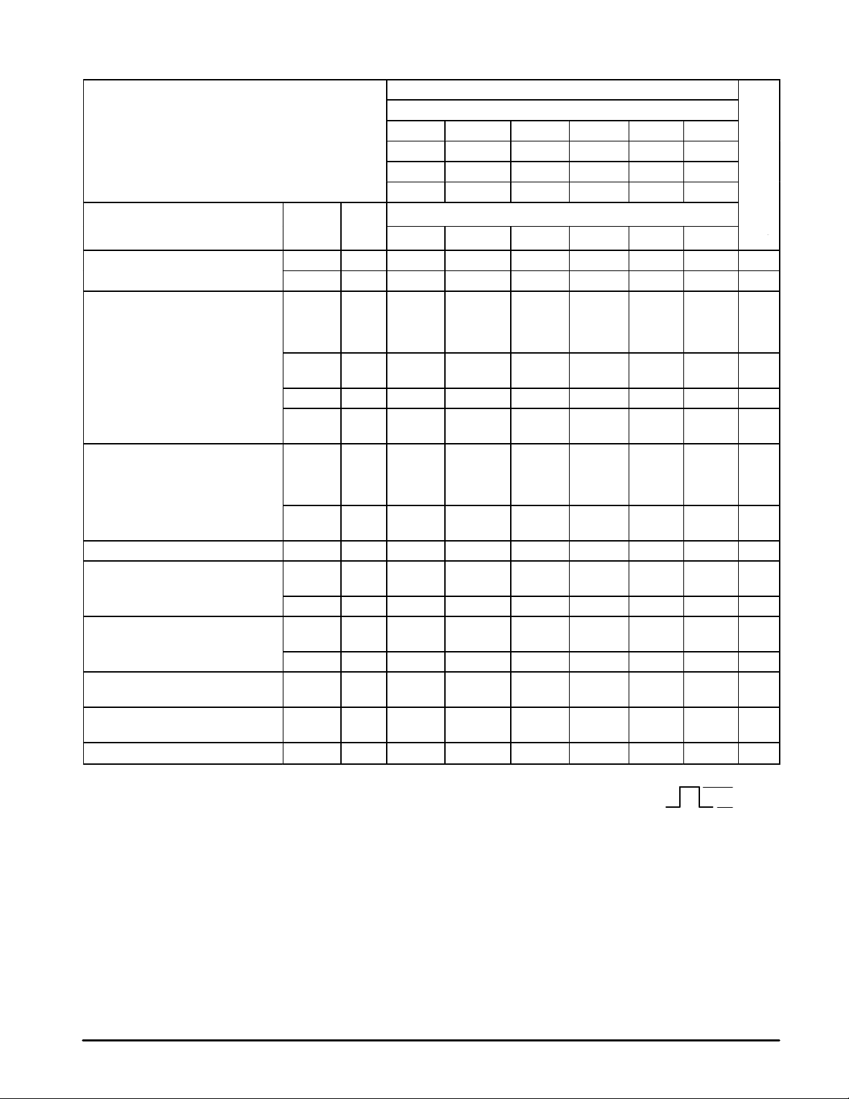
ELECTRICAL CHARACTERISTICS (Supply Voltage = –5.2 V, unless otherwise noted.) (continued)
TEST VOLTAGE/CURRENT VALUES
Volts
@ Test Temperature V
–30°C –0.890 –1.990 –1.205 –1.500 –2.8 –4.7
+25°C –0.810 –1.950 –1.105 –1.475 –2.8 –4.7
+85°C –0.700 –1.925 –1.035 –1.440 –2.8 –4.7
Pin
Characteristic Symbol
Power Supply Drain Current I
Input Current I
Leakage Current I
Reference Voltage V
Logic ‘1’ Output Voltage V
Logic ‘0’ Output Voltage V
Logic ‘1’ Threshold Voltage V
Logic ‘0’ Threshold Voltage V
Short Circuit Current I
1. Test outputs of the device must be tested by sequencing through the truth table. All input, power supply and
ground voltages must be maintained between tests. The clock input is the waveform shown.
2. In addition to meeting the output levels specified, the device must divide by 5, 8 or 10 during this test. The clock
input is the waveform shown.
3. In addition to meeting the output levels specified, the device must divide by 6, 9 or 11 during this test. The clock
input is the waveform shown.
CC1
I
CC2
inH1
I
inH2
I
inH3
I
inH4
inL1
I
inL2
BB
OH1
(Note 1.)23
V
OH2
OL1
(Note 1.)23
V
OL2
OHA
(Note 2.)23
OLA
(Note 3.)23
OS
Test
8 1,16
6 4 5 6
15
11
12
13
4
5
5 4 5 6
9
10
15
11
12
13
9
10
14 1,16
7 5 4 6
7 4 5 6
7 5 4 7 6
IHmax
er
V
IHmax
15
11
12
13
5
5
V
ILmin
TEST VOLTAGE APPLIED TO PINS LISTED BELOW
V
ILmin
4
4
11,12,13
11,12,13
11,12,13
11,12,13
V
IHAminVILAmax
V
IHAminVILAmax
11,12,13
11,12,13
11,12,13
11,12,13
V
IH
V
IH
9
10
Clock Input
V
ILH
V
10
9,10
9,10
9,10
9,10
Gnd
IL
1,16
1,16
1,16
1,16
6
6
1,16
1,16
1,16
1,16
1,16
1,16
9
1,16
1,16
1,16
1,16
1,16
1,16
1,16
1,16
1,16
1,16
V
IHmax
V
ILmin
4
MOTOROLA RF/IF DEVICE DATA
Page 5

MC12009 MC12011 MC12013
Und
ELECTRICAL CHARACTERISTICS (Supply Voltage = –5.2 V, unless otherwise noted.) (continued)
TEST VOLTAGE/CURRENT VALUES
Volts mA
@ Test Temperature V
–30°C –3.2 –4.4 –5.2 –0.25 16 –0.40
+25°C –3.2 –4.4 –5.2 –0.25 16 –0.40
+85°C –3.2 –4.4 –5.2 –0.25 16 –0.40
Pin
Characteristic Symbol
Power Supply Drain Current I
Input Current I
Leakage Current I
Reference Voltage V
Logic ‘1’ Output Voltage V
Logic ‘0’ Output Voltage V
Logic ‘1’ Threshold Voltage V
Logic ‘0’ Threshold Voltage V
Short Circuit Current I
1. Test outputs of the device must be tested by sequencing through the truth table. All input, power supply and
ground voltages must be maintained between tests. The clock input is the waveform shown.
2. In addition to meeting the output levels specified, the device must divide by 5, 8 or 10 during this test. The clock
input is the waveform shown.
3. In addition to meeting the output levels specified, the device must divide by 6, 9 or 11 during this test. The clock
input is the waveform shown.
CC1
I
CC2
inH1
I
inH2
I
inH3
I
inH4
inL1
I
inL2
BB
OH1
(Note 1.)23
V
OH2
OL1
(Note 1.)23
V
OL2
OHA
(Note 2.)23
OLA
(Note 3.)23
OS
Test
8 8 1,16
6 8 6
15
11
12
13
4
5
5 8 6
9
10
15
11
12
13
9
10
14 8 14 1,16
7 8 7 6
7 8 7 6
7 8 6
IHT
er
V
IHT
9,10
9,10
9,10
9,10
9,10
V
ILT
TEST VOLTAGE APPLIED TO PINS LISTED BELOW
V
ILT
9,10
9,10
V
EE
V
EE
8
8
8
8
8
8
8
8
8,15
8,11
8,12
8,13
8
8
8
8
8
8
8
8
8
8
I
L
I
L
I
OL
I
OL
Clock Input
I
I
OH
OH
Gnd
1,16
1,16
1,16
1,16
1,16
1,16
1,16
1,16
1,16
1,16
1,16
1,16
1,16
1,16
1,16
1,16
1,16
1,16
1,16
1,16
V
IHmax
V
ILmin
6
6
MOTOROLA RF/IF DEVICE DATA
5
Page 6

MC12009 MC12011 MC12013
Under
pp y
ELECTRICAL CHARACTERISTICS (Supply Voltage = 5.0 V, unless otherwise noted.)
Test Limits
Pin
Characteristic Symbol
Power Supply Drain Current
Input Current I
Leakage Current I
Reference Voltage V
Logic ‘1’ Output Voltage V
Logic ‘0’ Output Voltage V
Logic ‘1’ Threshold Voltage V
Logic ‘0’ Threshold Voltage V
Short Circuit Current I
4. Test outputs of the device must be tested by sequencing through the truth table. All input, power supply and
ground voltages must be maintained between tests. The clock input is the waveform shown.
5. In addition to meeting the output levels specified, the device must divide by 5, 8 or 10 during this test. The clock
input is the waveform shown.
6. In addition to meeting the output levels specified, the device must divide by 6, 9 or 11 during this test. The clock
input is the waveform shown.
I
CC1
I
CC2
inH1
I
inH2
I
inH3
I
inH4
inL1
I
inL2
BB
OH1
(Note 4.)
V
OH2
OL1
(Note 4.)
V
OL2
OHA
(Note 5.)
OLA
(Note 6.)
OS
Under
Test
8 –88 –80 –80 mAdc
6 5.2 5.2 5.2 mAdc
15
11
12
13
4
5
5 0.7 3.0 1.0 3.0 1.0 3.6
9
10
15
11
12
13
9
10
14 3.67 3.87 Vdc
2
3
7 2.4 2.6 2.8
2
3
7 0.94 0.80 0.72
2
3
2
3
7 –65 –20 –65 –20 –65 –20 mAdc
–30°C +25°C +85°C
Min Max Min Max Min Max
1.7
1.7
–10
–10
–10
–10
–1.6
–1.6
3.900
3.900
3.070
3.070
3.880
3.880
375
375
375
375
6.0
6.0
4.110
4.110
3.385
3.385
3.405
3.405
2.0
2.0
100
100
–10
–10
–10
–10
–1.6
–1.6
4.000
4.000
3.110
3.110
3.980
3.980
250
250
250
250
6.0
6.0
100
100
4.190
4.190
3.410
3.410
3.430
3.430
2.0
2.0
–10
–10
–10
–10
–1.6
–1.6
4.070
4.070
3.135
3.135
4.050
4.050
250
250
250
250
6.4
6.4
100
100
4.300
4.300
3.445
3.445
3.465
3.465
Clock Input
Unit
µAdc
mAdc
µAdc
µAdc
mAdc
Vdc
Vdc
Vdc
Vdc
V
IHmax
V
ILmin
Each MECL 10,000 series circuit has been designed to meet the dc specifications shown in the test table, after thermal equilibrium has been
established. The circuit is in a test socket or mounted on a printed circuit board and transverse air flow greater than 500 linear fpm is maintained.
Outputs are terminated through a 50 Ω resistor to –2.0 V. Test procedures are shown for only one gate. The other gates are tested in the same
manner.
6
MOTOROLA RF/IF DEVICE DATA
Page 7

MC12009 MC12011 MC12013
Und
ELECTRICAL CHARACTERISTICS (Supply Voltage = 5.0 V, unless otherwise noted.) (continued)
TEST VOLTAGE/CURRENT VALUES
Volts
@ Test Temperature V
–30°C +4.110 +3.070 +3.795 +3.500 +2.4 +0.5
+25°C +4.190 +3.110 +3.895 +3.525 +2.4 +0.5
+85°C +4.300 +3.135 +3.965 +3.560 +2.4 +0.5
Pin
Characteristic Symbol
Power Supply Drain Current I
Input Current I
Leakage Current I
Reference Voltage V
Logic ‘1’ Output Voltage V
Logic ‘0’ Output Voltage V
Logic ‘1’ Threshold Voltage V
Logic ‘0’ Threshold Voltage V
Short Circuit Current I
4. Test outputs of the device must be tested by sequencing through the truth table. All input, power supply and
ground voltages must be maintained between tests. The clock input is the waveform shown.
5. In addition to meeting the output levels specified, the device must divide by 5, 8 or 10 during this test. The clock
input is the waveform shown.
6. In addition to meeting the output levels specified, the device must divide by 6, 9 or 11 during this test. The clock
input is the waveform shown.
CC1
I
CC2
inH1
I
inH2
I
inH3
I
inH4
inL1
I
inL2
BB
OH1
(Note 4.)23
V
OH2
OL1
(Note 4.)23
V
OL2
OHA
(Note 5.)23
OLA
(Note 6.)23
OS
Test
8 8
6 4 5 8
15
11
12
13
4
5
5 4 5 8
9
10
15
11
12
13
9
10
14 8
7 5 4 8
7 4 5 8
7 5 4 7 8
IHmax
er
V
IHmax
15
11
12
13
5
5
V
ILmin
TEST VOLTAGE APPLIED TO PINS LISTED BELOW
V
ILmin
4
4
11,12,13
11,12,13
11,12,13
11,12,13
V
IHAminVILAmax
V
IHAminVILAmax
11,12,13
11,12,13
11,12,13
11,12,13
V
IH
V
IH
9
10
Clock Input
V
ILH
V
10
9,10
9,10
9,10
9,10
(VEE)
Gnd
IL
8
8
8
8
8
8
8
8
8,15
8,11
8,12
8,13
9
V
IHmax
V
ILmin
8
8
8
8
8
8
8
8
8
8
MOTOROLA RF/IF DEVICE DATA
7
Page 8

MC12009 MC12011 MC12013
Und
ELECTRICAL CHARACTERISTICS (Supply Voltage = 5.0 V, unless otherwise noted.) (continued)
TEST VOLTAGE/CURRENT VALUES
Volts mA
@ Test Temperature V
–30°C +2.0 +0.8 +5.0 –0.25 16 –0.40
+25°C +2.0 +0.8 +5.0 –0.25 16 –0.40
+85°C +2.0 +0.8 +5.0 –0.25 16 –0.40
Pin
Characteristic Symbol
Power Supply Drain Current I
Input Current I
Leakage Current I
Reference Voltage V
Logic ‘1’ Output Voltage V
Logic ‘0’ Output Voltage V
Logic ‘1’ Threshold Voltage V
Logic ‘0’ Threshold Voltage V
Short Circuit Current I
4. Test outputs of the device must be tested by sequencing through the truth table. All input, power supply and
ground voltages must be maintained between tests. The clock input is the waveform shown.
5. In addition to meeting the output levels specified, the device must divide by 5, 8 or 10 during this test. The clock
input is the waveform shown.
6. In addition to meeting the output levels specified, the device must divide by 6, 9 or 11 during this test. The clock
input is the waveform shown.
CC1
I
CC2
inH1
I
inH2
I
inH3
I
inH4
inL1
I
inL2
BB
OH1
(Note 4.)23
V
OH2
OL1
(Note 4.)23
V
OL2
OHA
(Note 5.)23
OLA
(Note 6.)23
OS
Test
8 1,16 8
6 6 8
15
11
12
13
4
5
5 6 8
9
10
15
11
12
13
9
10
14 1,16 14 8
7 6 7 8
7 6 7 8
7 6 8
IHT
er
V
IHT
9,10
9,10
9,10
9,10
9,10
V
ILT
TEST VOLTAGE APPLIED TO PINS LISTED BELOW
V
ILT
9,10
9,10
V
CC
V
CC
1,16
1,16
1,16
1,16
6
6
1,16
1,16
1,16
1,16
1,16
1,16
1,16
1,16
1,16
1,16
1,16
1,16
1,16
1,16
1,16
1,16
I
L
I
L
I
OL
I
OL
Clock Input
I
I
OH
OH
(VEE)
Gnd
8,15
8,11
8,12
8,13
V
IHmax
V
ILmin
8
8
8
8
8
8
8
8
8
8
8
8
8
8
8
8
8
8
8
MOTOROLA RF/IF DEVICE DATA
Page 9

MC12009 MC12011 MC12013
Under
Pulse
Pulse
Pulse
V
V
V
V
V
CC
SWITCHING CHARACTERISTICS
Pin
Characteristic Symbol
Propagation Delay
(See Figures 3 and 5)
Setup Time
(See Figures 4 and 5)
Release Time
(See Figures 4 and 5)
Toggle Frequency
(See Figure 6)
MC12009 : 5/6
MC12011 : 8/9
MC12013 : 10/11
*Test inputs sequentially, with Pulse Generator 2 or 3 as indicated connected to input under test, and the voltage indicated applied to the other input(s) of the same type ( i.e., MECL or MTTL).
{
V
IHmin
{
V
ILmin
–30°C
+1.03
+0.175 + 0.200 + 0.235 Vdc
Under
Test Min Typ Max Min Typ Max Min Typ Max Unit
t
t
t
t
2
2
7
7
1195.0
1195.0
2
—
—
—
—
5.0————
5.0————
440
500
500
15+ 2+
15+ 2–
t
5+ 7+
t
5– 7–
setup1
setup2
t
rel1
t
rel2
f
max
+25°C +85°C
+1.115 + 1.20 Vdc
MC12009, MC12011, MC12013 TEST VOLTAGES/WAVEFORMS APPLIED TO PINS LISTED BELOW:
–30°C +25°C +85°C
—
8.1
—
—
8.1
—
—
7.5
—
—
—
8.4
6.5
—
—
—
—
—
5.0
5.0————
5.0
5.0————
480
550
550
—
—
—
—
7.5
—
8.1
—
6.5
—
—
—
—
—
—
—
—
—
—
—
—
—
5.0
5.0————nsns1515*—
5.0
5.0————nsns1515*—
440
—
500
—
500
—
8.9
8 2
8.9
7.1
—
—
—
Pulse Pulse Pulse V
Gen.1
ns 15
MHz
Gen.2
15
A
A
—
—
—
IHminVILminVFVEE
IHmin
Gen.3
—
—
—
—
—
—
—
—
—*—
—*—
—
—
—
—
—
—
ILmin
{
{
—
11,12,13
—
11,12,13
—
—
—
—
—*11,12,13
—*11,12,13
11
—
11
—
11
—
–3.0 V
9,10
9,10
—
—
9,10*881,6,16
9.10*881,6,16
—
—
—
F
–3.0 V
Figure 3. AC Voltage Waveforms
Pulse
Generator
1
Q (Pin 2)
(Pin 3)
Q
t++
t+ –
50%
50%
50%
80%
20%
V
IHmin
V
ILmin
V
EE
+2.0
8
1,6,16
8
1,6,16
8
1,6,16
8
1,6,16
1,6,16
1,6,16
8
16
8
16
8
16
Pulse
Generator
1
Pulse
Generator
2
Pulse
Generator
3
Q (Pin 2)
t
setup1
t
setup2
+1.5 V
+In
MTTL
50%
t++
t––
Out
–1.5 V
Figure 4. Setup and Release Time Waveforms
V
80%
50
%
80%
50%
20%
20%
90%
10%
Divide by 5 — MC12009
Divide by 8 — MC12011
Divide by 10 — MC12013
IHmin
V
ILmin
V
IHmin
V
ILmin
0 V
V
EE
Pulse
Generator
1
Pulse
Generator
2
Pulse
Generator
3
Q (Pin 2)
50%
t
rel2
–1.5 V
80%
20%
90%
10%
80%
20%
50%
t
rel1
Divide by 6 — MC12009
Divide by 9 — MC12011
Divide by 11 — MC12013
V
IHmin
V
ILmin
V
IHmin
V
ILmin
0 V
V
EE
MOTOROLA RF/IF DEVICE DATA
9
Page 10

MC12009 MC12011 MC12013
Figure 5. AC Test Circuit
V
V
in
VCC = +2.0 V
(Scope Channel B)
out
Pulse
Generator
#1
Pulse
Generator
#2
MC10109 or equiv.
A
50
100
Pulse
Generator
#3
V
in
50
100
V
in
(Scope Channel A)
V
in
950
50
25
0.1
µ
µ
F
13
12
11
10
15
14
9
5
1616
E1
E2
E3
E4
E5
C
V
BB
+
MECL
Q
Q
F
2
3
V
out
V
out
1950
to
4
MTTL
–
Trans–
7
lator
8
µ
F
0.1
C
T
VEE = –3.0 V
All Pulse Generators are EH 137 or equiv.
Pulse Generators 1 and 2:
PRF = 10 MHz
PW = 50% Duty Cycle
t+ = t – = 2.0 ± 0.2 ns
Pulse Generator 3:
PRF = 2.0 MHz
PW = 50% Duty Cycle
t+ = t – = 5.0 ± 0.5 ns
50
VEE = –3.0 V
All resistors are + 1%.
All input and output cables to the scope are equal lengths of 50–ohm coaxial cable.
The 1950–ohm resistor at Pin 7 and the scope termination impedance constitute a 40:1 attenuator probe.
CT = 15 pF = total parasitic capacitance which includes probe, wiring, and load capacitance.
Unused output connected to a 50–ohm resistor to ground.
10
MOTOROLA RF/IF DEVICE DATA
Page 11

MC12009 MC12011 MC12013
Figure 6. Maximum Frequency T est Circuit
Sine Wave
Input
(T o Scope)
V
= +2.0 V
CC
0.1
µ
F
116
13
V
in
V
EE
0.1
µ
F
1 k
12
10
15
14
0.1
0.1
E1
E2
11
E3
E4
9
E5
C
V
BB
µ
F
8
µ
F
VEE = –3.0 V
Unused output connected to a 50 Ω resistor to ground
5.0 µF
2
Q
3
Q
V
out
to
Scope
Clock
Input
Q (Pin 2)
Clock
Input
Q (Pin 2)
Clock
Input
800 mV
3 Cycles 3 Cycles
800 mV
5 Cycles 4 Cycles
800 mV
DIVIDE BY 6
850 mV typ
DIVIDE BY 9
850 mV typ
DIVIDE BY 11
850 mV typ
Q (Pin 2)
MOTOROLA RF/IF DEVICE DATA
5 Cycles6 Cycles
11
Page 12

Enable = 0
Q1 Q2 Q3
1 1 1
0 1 1
0 0 1
0 0 0
1 0 0
1 1 0
MC12009 MC12011 MC12013
Figure 7. State Diagram
DIVIDE BY 5/6 (MC12009/MC12509)
111 011 001
Enable = 1
110 100 000
010 101
Enable = 0
Enable = 1
Q1 Q2 Q3 Q4
1 1 1 1
0 1 1 1
0 0 1 1
1 0 0 1
1 1 0 1
0 1 1 0
0 0 1 0
1 0 0 0
1 1 0 0
Enable = 1.
DIVIDE BY 8/9 (MC12011)
Enable = 1
DIVIDE BY 10/11 (MC12013)
0101 0010 1000 1100 1010
1110 0110 0000 0111 1111
0001
1101 1001 0011
1011 0100
1110
Q1 Q2 Q3 Q4
1 1 1 1
0 1 1 1
0 0 1 1
0 0 0 1
1 0 0 1
Enable = 0
1 1 0 1
0 1 1 0
0 0 1 0
0 0 0 0
1 0 0 0
1 1 0 0
NOTES:
Enable = 1.
The State of the Enable is important only
Clock Transition when the counter is in state 1 100.
12
Enable = 1
for the positive
1001
0001
0011
1101
0111
0100
0110
0101
1011
1010
1100
1111
0010
0000
1000
MOTOROLA RF/IF DEVICE DATA
Page 13

MC12009 MC12011 MC12013
APPLICATIONS INFORMATION
The primary application of these devices is as a
high–speed variable modulus prescaler in the divide by N
section of a phase–locked loop synthesizer used as the
local oscillator of two–way radios.
Proper VHF termination techniques should be followed
when the clock is separated from the prescaler by any
appreciable distance.
In their basic form, these devices will divide by 5/6, 8/9,
or 10/1 1. Division by 5, 8, or 10 occurs when any one or all
Figure 8. Divide By 10/11 (MC12013)
13
12
11
10
9
15
5
4
E1
E2
E3
E4
E5
C
+
MECL
to
MTTL
Trans–
–
lator
Q4
Q
2
3
4
7
of the five gate inputs E1 through E5 are high. Division by
6, 9, or 11 occurs when all inputs E1 through E5 are low.
(Unconnected MTTL inputs are normally high, unconnected MECL inputs are normally low). With the addition
of extra parts, many different division configurations may
be obtained (20/21, 40/41, 50/51, 100/101, etc.) A few of
the many configurations are shown below, only for the
MC12013.
Q1 Q2 Q3 Q4
1 1 1 1
0 1 1 1
0 0 1 1
0 0 0 1
1 0 0 1
Enable = 0
1 1 0 1
0 1 1 0
0 0 1 0
0 0 0 0
1 0 0 0
1 1 0 0
Enable = 1
MOTOROLA RF/IF DEVICE DATA
13
Page 14

MC12009 MC12011 MC12013
Figure 9. Divide By 20/21 (MC12013)
COUNT Q1 Q2 Q3 Q4 Q4
31 1 1 1 1 1
30 0 1 1 1 1
13
12
11
10
9
15
5
4
E1
E2
E3
E4
E5
C
+
–
D
C
1/2 MC10131
MECL
to
MTTL
Trans–
lator
Q4
Q
2
3
4
E2 + E3 + E4 + E5 = 0
7
Q5
Q
Q
To obtain an MTTL output, connect Pins 5 and 4 to Pins 2 and 3 respectively. Termination
resistors for the MECL outputs are not shown, but are required except for the flip–flop driving
the translator section.
The B20/21 counter may also be built using an MTTL flip–flop by connecting Pins 5 and
4 to Pins 2 and 3 respectively, and driving the MTTL flip–flop with Pin 7. MC12013 inputs
E4 and E5 are used rather than E1. With E1 + E2 + E3 = 0, operation remains as shown.
28 0 0 1 1 1
24 0 0 0 1 1
25 1 0 0 1 1
27 1 1 0 1 1
22 0 1 1 0 1
20 0 0 1 0 1
16 0 0 0 0 1
17 1 0 0 0 1
19 1 1 0 0 1
14 0 1 1 1 0
12 0 0 1 1 0
8 0 0 0 1 0
9 1 0 0 1 0
11 1 1 0 1 0
6 0 1 1 0 0
4 0 0 1 0 0
0 0 0 0 0 0
1 1 0 0 0 0
3 1 1 0 0 0
E2 + E3 + E4 + E5 = 1
Figure 10. Divide By 40/41 (MC12013)
13
12
11
10
9
15
5
4
E1
E2
E3
E4
E5
C
+
MECL
to
MTTL
Trans–
–
lator
Q4
Q
2
D
C
3
4
7
D
C
Q
Q
Q
Q
MC10131
ForB40 : E4 + E5 = 1
ForB41: E4 + E5 = 0
Termination resistors for MECL
outputs are not shown, but are
required except for the flip–flop
driving the translator section.
14
MOTOROLA RF/IF DEVICE DATA
Page 15
MC12009 MC12011 MC12013
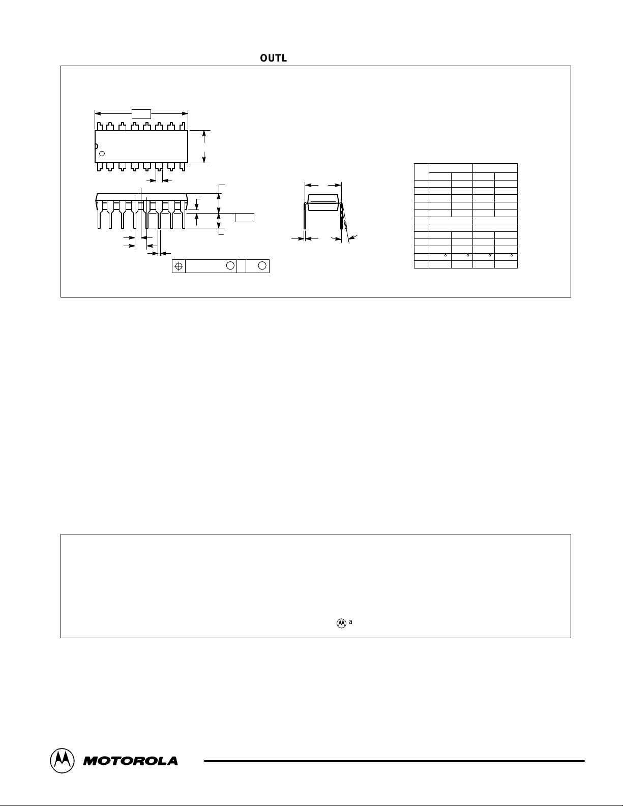
OUTLINE DIMENSIONS
PLASTIC PACKAGE
CASE 648–08
–A–
916
B
18
F
H
G
D
16 PL
0.25 (0.010) T
C
S
SEATING
–T–
PLANE
K
M
A
J
M
P SUFFIX
ISSUE R
L
NOTES:
1. DIMENSIONING AND TOLERANCING PER ANSI
Y14.5M, 1982.
2. CONTROLLING DIMENSION: INCH.
3. DIMENSION L TO CENTER OF LEADS WHEN
FORMED PARALLEL.
4. DIMENSION B DOES NOT INCLUDE MOLD FLASH.
5. ROUNDED CORNERS OPTIONAL.
DIM MIN MAX MIN MAX
A 0.740 0.770 18.80 19.55
B 0.250 0.270 6.35 6.85
C 0.145 0.175 3.69 4.44
D 0.015 0.021 0.39 0.53
F 0.040 0.70 1.02 1.77
G 0.100 BSC 2.54 BSC
M
H 0.050 BSC 1.27 BSC
J 0.008 0.015 0.21 0.38
K 0.110 0.130 2.80 3.30
L 0.295 0.305 7.50 7.74
M 0 10 0 10
S 0.020 0.040 0.51 1.01
MILLIMETERSINCHES
____
Motorola reserves the right to make changes without further notice to any products herein. Motorola makes no warranty , representation or guarantee regarding
the suitability of its products for any particular purpose, nor does Motorola assume any liability arising out of the application or use of any product or circuit, and
specifically disclaims any and all liability, including without limitation consequential or incidental damages. “T ypical” parameters which may be provided in Motorola
data sheets and/or specifications can and do vary in different applications and actual performance may vary over time. All operating parameters, including “Typicals”
must be validated for each customer application by customer’s technical experts. Motorola does not convey any license under its patent rights nor the rights of
others. Motorola products are not designed, intended, or authorized for use as components in systems intended for surgical implant into the body, or other
applications intended to support or sustain life, or for any other application in which the failure of the Motorola product could create a situation where personal injury
or death may occur. Should Buyer purchase or use Motorola products for any such unintended or unauthorized application, Buyer shall indemnify and hold Motorola
and its officers, employees, subsidiaries, affiliates, and distributors harmless against all claims, costs, damages, and expenses, and reasonable attorney fees
arising out of, directly or indirectly, any claim of personal injury or death associated with such unintended or unauthorized use, even if such claim alleges that
Motorola was negligent regarding the design or manufacture of the part. Motorola and are registered trademarks of Motorola, Inc. Motorola, Inc. is an Equal
Opportunity/Affirmative Action Employer.
How to reach us:
USA/EUROPE/ Locations Not Listed: Motorola Literature Distribution; JAPAN: Nippon Motorola Ltd.: SPD, Strategic Planning Office, 141,
P.O. Box 5405, Denver, Colorado 80217. 1–303–675–2140 or 1–800–441–2447 4–32–1 Nishi–Gotanda, Shagawa–ku, Tokyo, Japan. 03–5487–8488
Customer Focus Center: 1–800–521–6274
Mfax: RMFAX0@email.sps.mot.com – TOUCHTONE 1–602–244–6609 ASIA/PACIFIC: Motorola Semiconductors H.K. Ltd.; 8B T a i Ping Industrial Park,
Moto rola Fa x Back System – US & Canada ONLY 1–800–774–1848 51 Ting Kok Road, Tai Po, N.T., Hong Kong. 852–26629298
HOME PAGE: http://motorola.com/sps/
MOTOROLA RF/IF DEVICE DATA
– http://sps.motorola.com/mfax/
◊
Mfax is a trademark of Motorola, Inc.
12009/D
15
 Loading...