

Page 1
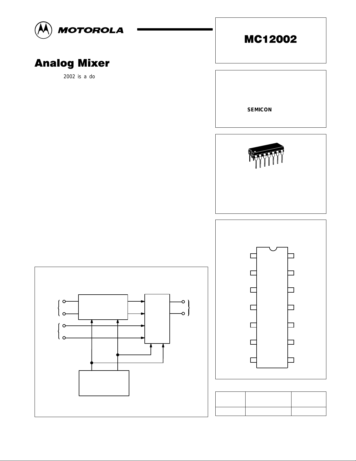
The MC12002 is a double balanced analog mixer, including an input
amplifier feeding the mixer carrier port and a temperature compensated bias
regulator. The input circuits for both the amplifier and mixer are differential
amplifier circuits. The on-chip regulator provides all of the required biasing.
This circuit is designed for use as a balanced mixer in high-frequency
wide-band circuits. Other typical applications include suppressed carrier and
amplitude modulation, synchronous AM detection, FM detection, phase
detection, and frequency doubling, at frequencies up to UHF.
Order this document by MC12002/D
ANALOG MIXER
SEMICONDUCTOR
TECHNICAL DATA
14
1
Local
Oscillator
Inputs
Signal
Inputs
P SUFFIX
PLASTIC PACKAGE
CASE 646
PIN CONNECTIONS
Regulator
Bypass
Local Oscillator
Input
1
2
14 V
13
CC
Resistor Load
Figure 1. Logic Diagram
Local Oscillator
2
3
8
9
Amplifier
V
B
Regulator
Bias
V
R
Carrier
Port
Mixer
Signal
Port
VRV
12
Output
11
B
Alternate Signal
Device
MC12002P TA = –30° to +85°C Plastic
Input
Input
Null Adjust
Null Adjust
V
ORDERING INFORMATION
3
4
5
6
78
EE
Operating
Temperature Range
(Top View)
12
Data Output
11
Data Output
10
Regulator
Bypass
9
Mixer Signal
Input
Mixer Signal
Input
Package
Motorola, Inc. 1997 Rev 5
Page 2

ELECTRICAL CHARACTERISTICS
Under
Pin
Under
CC
inH
I
inL
IO
IO
I
out
Bias
A
Test
14 — — — 16 — — mAdc — — 11,12,14 5,6,7
1112————0.7
1
1112————2.1
2
11
11
12
12
11,12
1
11,12
2
10
11 — — 5.0 — — — V/V 2 11 9 14 7
V
11 — — 0.28 — — — V/V 8 11 3 14 7
Characteristic Symbol
Power Supply Drain I
Input Current
Output Current
Differential Current ∆IO
Bias Voltage V
AC Gain (See Figure 1)
(Frequency =
100 MHz) *Note
NOTE: *Note: AC Gain is a function of collector load impedance.
I
∆IO
–30°C +25°C +85°C
Min Max Min Max Min Max Unit
2
—
—
—
—
—
—
—
—
—
—
—
—
–100
–200
2.33
390
275
275
1.26
—
—
—
—
—
—
—
—
—
—
—
—
+100
+200
2.53
590
415
415
1.46
3
8
9
2
3
8
9
1
4
5
6
MC12002
Test Limits
—
—
—
—
– 0.7
– 0.7
– 0.7
– 0.7
0.7
2.1
4.2
4.2
4.2
4.2
–100
–200
2.32
400
285
285
1.185
1.385
0.75
0.75
0.75
0.75
+100
+200
2.52
600
425
425
—
—
—
—
—
—
—
—
—
—
—
—
1.3
1.3————
3.9
3.9————
7.8
— —
7.8
7.8
7.8
–100
–200
2.3
410
295
295
1.105
—
—
—
—
—
—
—
—
—
—
—
+100
+200
2.5
610
435
435
1.305
TEST VOLTAGE VALUES
V
IHmaxVILminVCC
+2.9 +2.0 +5.0
VOLTAGE APPLIED TO PINS
LISTED BELOW
V
IHmaxVILminVCC
mAdc
mAdc
mAdc
mAdc
mAdc
mAdc
mAdc
mAdc
mAdc
mAdc
mAdc
mAdc
mAdc
mAdc
mAdc
mAdc
µAdc
µAdc
Vdc
mVdc
mVdc
mVdc
Vdc
2
3
8
9
—
—
—
—
—
—
—
—
2,9
3,8
2,8
3,9
—
—
—
—
—
—
—
PulseInPulse
Out
Volts
—
11,12,14
—
11,12,14
—
11,12,14
—
11,12,14
2
11,12,14
3
11,12,14
8
11,12,14
9
11,12,14
——11,12,14
11,12,1477
——11,12,14
11,12,14
—
11,12,14
—
11,12,14
—
11,12,14
—
11,12,14
——11,12,14
11,12,1475,6,7
—
11,12,14
—
11,12,14
—
11,12,14
—
11,12,14
—
11,12,14
–3.0 V Gnd V
Gnd
5,6,7
5,6,7
5,6,7
5,6,7
5,6,7
5,6,7
5,6,7
5,6,7
5,6,7
5,6,7
5,6,7
5,6,7
5,6,7
5,6,7
5,6,7
5,6,7
7
7
5,6,7
EE
2
MOTOROLA RF/IF DEVICE DATA
Page 3
MC12002
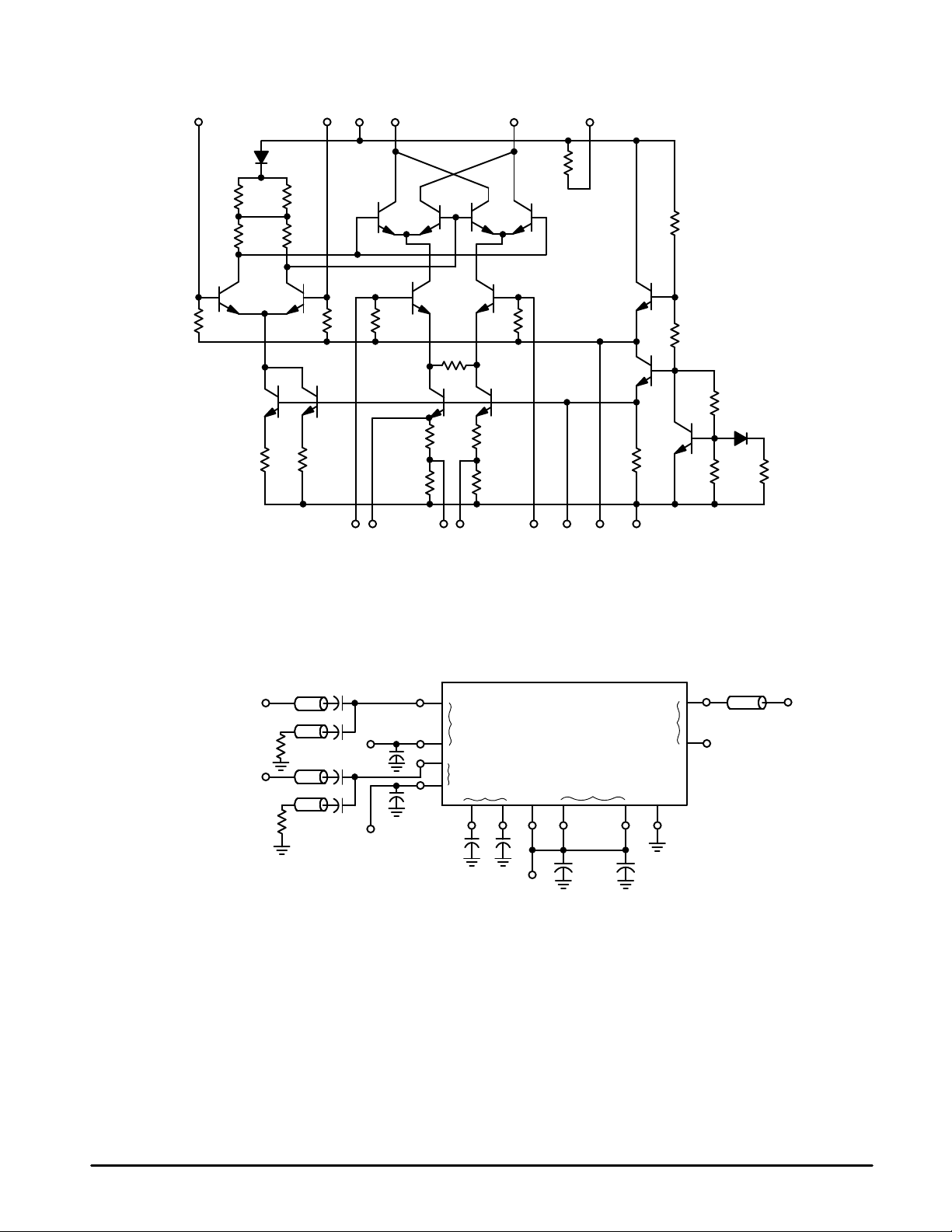
Figure 2. Analog Mixer Circuit Schematic
1 k
2
6767
67 67
167167
1 k
1 k1 k
100
167 167
333333
12
133
1095648
1311143
663
17
493
318
880
350631
0.1
µ
f
Signal A
50
Signal B
50
Note 1:
VIL= –3.0 V on pin 3 when pin 8 is under test.
VIL= –3.0 V on pin 9 when pin 2 is under test.
Signal A = 30 mVpp
Signal B = 300 mVpp
Freq. = 100 MHz
0.1
0.1
0.1
µ
f
Note 1
µ
f
µ
F
0.1
µ
Note 1
Figure 3. AC Gain Test
2
Local Oscillator
Inputs
3
8
f
0.1
9
µ
f
0.1
Mixer
Inputs
Reg. Bypass
µ
F
V
0.1
µ
F
–5.0V
EE
12
Outputs
Null
Adj.
57110
614
10
11
V
CC
µ
F0.1µf
All input and output
cables to the scope are
equal lengths of 50-ohm
coaxial cable.
The unused output is
connected to a 50-ohm
resistor to ground.
MOTOROLA RF/IF DEVICE DATA
3
Page 4

Figure 4. Carrier Feedthrough Test Circuits
Signal A
Input (Pin 2)
Output (Pin12)
Output (Pin 11)
Signal B Input (Pin 8)
Output (Pin 12)
MC12002
Output (Pin 11)
T ektronix
454 and 568
Oscilloscopes
Hewlett Packard
651A and 3300B
100 kHz to 100 MHz
@ 30 mVpp
Notes:
Test 1– Adjust potentiometer for carrier null at fc = 100 kHz.
Test 2– Connect pins 5 and 6 to Gnd.
1.0µf
1.0
1.0
2
Local Oscillator
3
µ
f
0.1
8
9
µ
f
µ
f
Inputs
Reg.
Bypass
µ
0.1
Mixer
Inputs
f
V
EE
Null
Adjust
50
Outputs
V
CC
61457110
+5.0 V
All Input and output
cables to the scope are
equal lengths of 50-ohm
coaxial cable.
12
11
133 133
0.1
µ
f
Sampling Volt meter
Hewlett Packard
3406A or Equiv.
4
MOTOROLA RF/IF DEVICE DATA
Page 5

MC12002
Figure 5. Carrier Feedthrough versus Frequency
(Test 1)
5.0
4.0
3.0
2.0
1.0
CFT
V , CARRIER OUTPUT VOL TAGE (mV[rms])
0.0
fc, CARRIER FREQUENCY (MHz)
Figure 7. Carrier Suppression T est Circuit
Hewlett Packard 3406A
Sampling Voltmeter
µ
f
0.1
TEE 11536A
Hewlett Packard
651A and 3300B
100 kHz to 400 MHz
@ 30 mV RMS.
Hewlett
Packard
Hewlett Packard
651A 10 kHz
@ 150 mV R.M.S.
50
Notes:
µ
f
1.0
µ
f
0.1
1.0
µ
f
Test 1 – Adjust potentiometer for carrier null @ fc = 100 kHz
Test 2 – Connect pins 5 and 6 to –5.0 volts
Test 3 – Adjust potentiometer for carrier null @ 25° C
2
Local Oscillator
3
8
Mixer
9
Inputs
1.0
µ
f
100.010.01.00.1
Inputs
1.0
Figure 6. Carrier Feedthrough versus Frequency
(Test 2)
5.0
4.0
3.0
2.0
1.0
CFT
V , CARRIER OUTPUT VOL TAGE (mV [rms])
0.0
0.1
fc, CARRIER FREQUENCY (MHz)
12
µ
f
–
+
Reg.
Bypass
V
EE
– 5.0 V
Null
Adjust
50
– 5.0 V
Outputs
14657101
11
50
V
CC
All input and output
cables to the scope are
equal lengths of 50-ohm
coaxial cable.
10.0 100.01.0
50
X 50
Atten.
50
50
Figure 8. Carrier Suppression versus Frequency
(Test 1)
+40
+30
+20
+10
0
–10
–20
–30
CARRIER SUPPRESSION (dB)
–40
–50
–60
0.1 1.0
fc, CARRIER FREQUENCY (MHz)
MOTOROLA RF/IF DEVICE DATA
Figure 9. Carrier Suppression versus Frequency
(Test 2)
+40
+30
+20
+10
0
–10
–20
–30
CARRIER SUPPRESSION (dB)
–40
–50
–60
1.0K100.010.0
1.0K100.010.01.00.1
fc, CARRIER FREQUENCY (MHz)
5
Page 6

MC12002
Figure 10. Carrier Suppression versus T emperature
–10
–20
–30
fc = 10 MHz @ 30 mv
fs = 10 KHz @ 150 mv
–40
–50
CARRIER SUPPRESSION (dB)
rms
rms
–60
TA, AMBIENT TEMPERATURE (°C)
Figure 11. Output Offset Current (I00) versus T emperature
1.0
µ
f
2
0.1
3
8
9
µ
f
Local Oscillator
Inputs
Mixer
Inputs
Reg.
Bypass
101
0.1
Outputs
Null
V
EE
7
µ
f
µ
f
0.1
Adjust
56
1.0
1.0
1.0
µ
f
µ
f
µ
f
+125+100+75+50+250–25–55
I
12
12
I
µ
A
I
11
11
I
µ
A
V
CC
14
IOO = I11 – I
12
Notes:
–5.0 V
Test 1 – Pins 5 and 6 left open
Test 2 – Pins 5 and 6 are tied to –5.0 volts
Figure 12. Output Offset Current versus T emperature Figure 13. Typical Input Impedance versus Frequency
(No Circuit)
400
+100
µ
OO
I , OUTPUT OFFSET CURRENT ( A)
–100
+50
0.0
–50
TEST 1
TEST 2
+125+100+75+50+250–25–55
TA, AMBIENT TEMPERATURE (°C)
350
300
250
200
150
L
100
R RESISTANCE (Ohms)
50
R(OHMS)
TYPICAL INPUT IMPEDANCE
Z
vs
FREQUENCY
R
in
C
– LOCAL OSCILLAT OR –
C
R
AND SIGNAL INPUTS
400200
f, FREQUENCY (MHZ)
1000800600
31
26
C, CAPACITANCE (pF)
21
16
11
6
1
6
MOTOROLA RF/IF DEVICE DATA
Page 7

MC12002
OUTLINE DIMENSIONS
P SUFFIX
PLASTIC PACKAGE
CASE 646–06
ISSUE M
14 8
B
17
NOTES:
1. DIMENSIONING AND TOLERANCING PER ANSI
Y14.5M, 1982.
2. CONTROLLING DIMENSION: INCH.
3. DIMENSION L TO CENTER OF LEADS WHEN
FORMED PARALLEL.
4. DIMENSION B DOES NOT INCLUDE MOLD FLASH.
5. ROUNDED CORNERS OPTIONAL.
–T–
SEATING
PLANE
N
HG
A
F
L
C
D
14 PL
0.13 (0.005)
K
J
M
M
DIM MIN MAX MIN MAX
A 0.715 0.770 18.16 18.80
B 0.240 0.260 6.10 6.60
C 0.145 0.185 3.69 4.69
D 0.015 0.021 0.38 0.53
F 0.040 0.070 1.02 1.78
G 0.100 BSC 2.54 BSC
H 0.052 0.095 1.32 2.41
J 0.008 0.015 0.20 0.38
K 0.115 0.135 2.92 3.43
L
0.290 0.310 7.37 7.87
M ––– 10 ––– 10
N 0.015 0.039 0.38 1.01
MILLIMETERSINCHES
__
MOTOROLA RF/IF DEVICE DATA
7
Page 8

MC12002
Motorola reserves the right to make changes without further notice to any products herein. Motorola makes no warranty , representation or guarantee regarding
the suitability of its products for any particular purpose, nor does Motorola assume any liability arising out of the application or use of any product or circuit, and
specifically disclaims any and all liability, including without limitation consequential or incidental damages. “T ypical” parameters which may be provided in Motorola
data sheets and/or specifications can and do vary in different applications and actual performance may vary over time. All operating parameters, including “Typicals”
must be validated for each customer application by customer’s technical experts. Motorola does not convey any license under its patent rights nor the rights of
others. Motorola products are not designed, intended, or authorized for use as components in systems intended for surgical implant into the body, or other
applications intended to support or sustain life, or for any other application in which the failure of the Motorola product could create a situation where personal injury
or death may occur. Should Buyer purchase or use Motorola products for any such unintended or unauthorized application, Buyer shall indemnify and hold Motorola
and its officers, employees, subsidiaries, affiliates, and distributors harmless against all claims, costs, damages, and expenses, and reasonable attorney fees
arising out of, directly or indirectly, any claim of personal injury or death associated with such unintended or unauthorized use, even if such claim alleges that
Motorola was negligent regarding the design or manufacture of the part. Motorola and are registered trademarks of Motorola, Inc. Motorola, Inc. is an Equal
Opportunity/Affirmative Action Employer.
How to reach us:
USA/EUROPE/Locations Not Listed: Motorola Literature Distribution; JAPAN: Nippon Motorola Ltd.: SPD, Strategic Planning Office, 141,
P.O. Box 5405, Denver, Colorado 80217. 1–303–675–2140 or 1–800–441–2447 4–32–1 Nishi–Gotanda, Shagawa–ku, Tokyo, Japan. 03–5487–8488
Customer Focus Center: 1–800–521–6274
Mfax: RMFAX0@email.sps.mot.com – TOUCHTONE 1–602–244–6609 ASIA/PACIFIC: Motorola Semiconductors H.K. Ltd.; 8B Tai Ping Industrial Park,
Moto rola Fax Back Sys tem – US & Canada ONLY 1–800–774–1848 51 Ting Kok Road, Tai Po, N.T., Hong Kong. 852–26629298
HOME PAGE: http://motorola.com/sps/
8
– http://sps.motorola.com/mfax/
◊
Mfax is a trademark of Motorola, Inc.
MOTOROLA RF/IF DEVICE DATA
MC12002/D
 Loading...