

Page 1
MC10SX1190
Product Preview
Fibre Channel Coaxial
Cable Driver and Loop
Resiliency Circuit
The MC10SX1190 is a differential receiver, differential transmitter
specifically designed to drive coaxial cables. It incorporates the output
cable drive capability of the MC10EP89 Coaxial Cable Driver with
additional circuitry to multiplex the output cable drive source between
the cable receiver or the local transmitter inputs. The multiplexer
control circuitry is TTL compatible for ease of operation.
The MC10SX1190 is useful as a bypass element for Fibre
Channel-Arbitrated Loop (FC-AL) or Serial Storage Architecture
(SSA) applications, to create loop style interconnects with fault
tolerant, active switches at each device node. This device is
particularly useful for back panel applications where small size is
desirable.
The EP89 style drive circuitry produces swings approximately 70%
larger than a standard PECL output. When driving a coaxial cable,
proper termination is required at both ends of the line to minimize
reflections. The 1.4V output swings allow for proper termination at
both ends of the cable, while maintaining the required swing at the
receiving end of the cable. Because of the larger output swings, the
QT, QT
VCC– 3.0V instead of 50Ω to VCC– 2.0V.
• 2.5 Gbps Operation
• 425ps Propagation Delay
• 1.4V Output Swing on the Cable Driving Output
• PECL Mode: 3.0V to 5.5V V
• ECL Mode: 0V V
• 75kΩ Internal Input Pull Down Resistors
• >1000 Volt ESD Protection
outputs are terminated into the thevenin equivalent of 50Ω to
, with VEE = 0V
CC
, with VEE = –3.0V to –5.5V
CC
V
V
V
CC
QR QR
CC
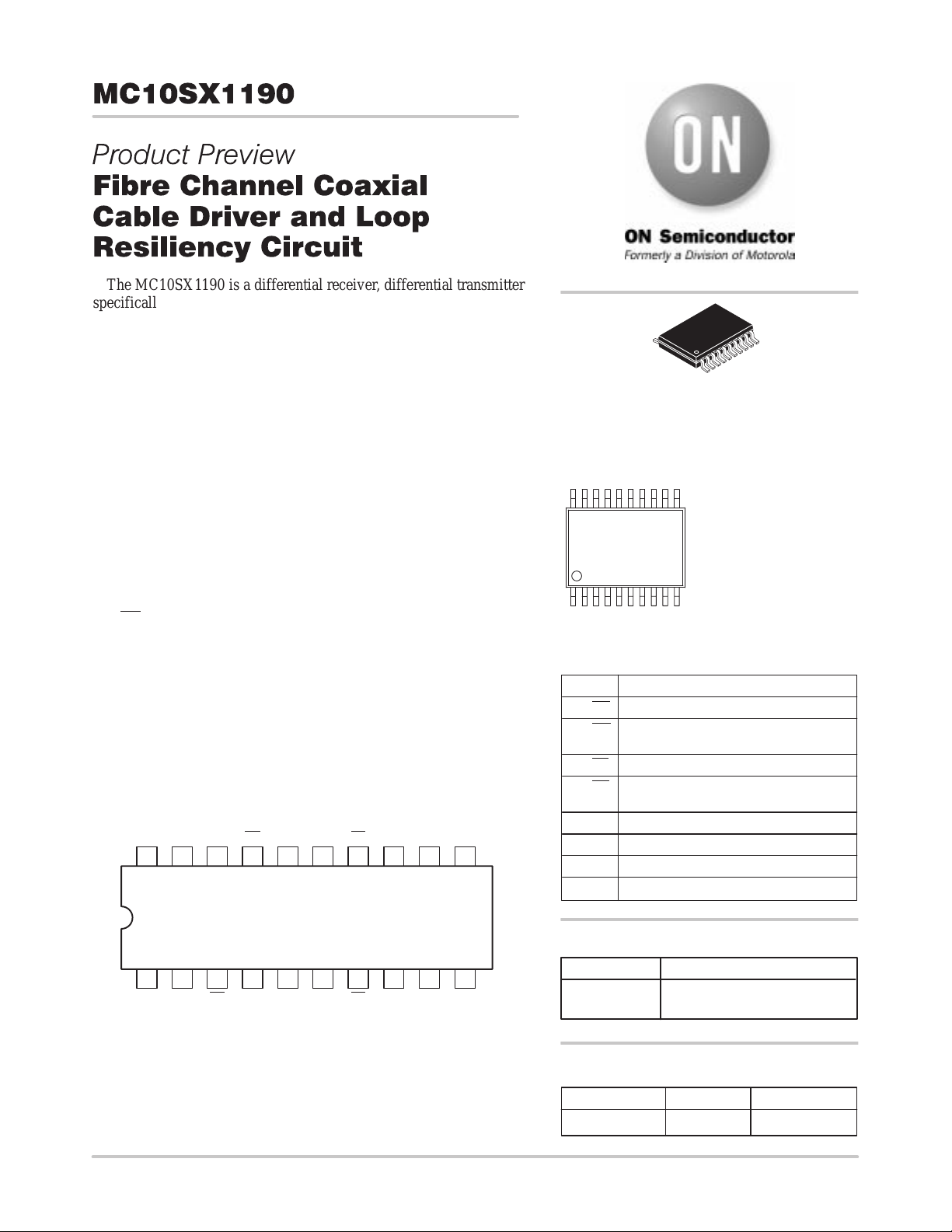
1920 18 17 16 15 14
EE
DT DT V
13
CC
VBBV
12911
EE
http://onsemi.com
20
1
TSSOP–20
DT SUFFIX
CASE 948E
MARKING DIAGRAM
10SX
1190
ALYW
*For additional information, see Application Note
AND8002/D
PIN DESCRIPTION
PIN
DR/DR
QR/QR ECL Buffered Differential Outputs from
DT/DT
QT/QT ECL Buffered Differential Output to
SEL
V
V
V
ECL Diff. Inputs from Receive Cable
Receive Cable
ECL Differential Input to Transmit Cable
Transmit Cable
TTL Multiplexer Control Signal
Reference Voltage Output
BB
ECL Positive Supply
CC
ECL Negative, 0 Supply
EE
A = Assembly Location
L = Wafer Lot
Y = Y ear
W = Work Week
FUNCTION
21 34567
V
DR DR
EE
Figure 1. 20-Lead TSSOP Pinout: (Top View)
This document contains information on a product under development. ON Semiconductor
reserves the right to change or discontinue this product without notice.
Semiconductor Components Industries, LLC, 1999
December, 1999 – Rev. 1
VCCV
CC
QT QT V
8
EE
SEL V
10
CC
1 Publication Order Number:
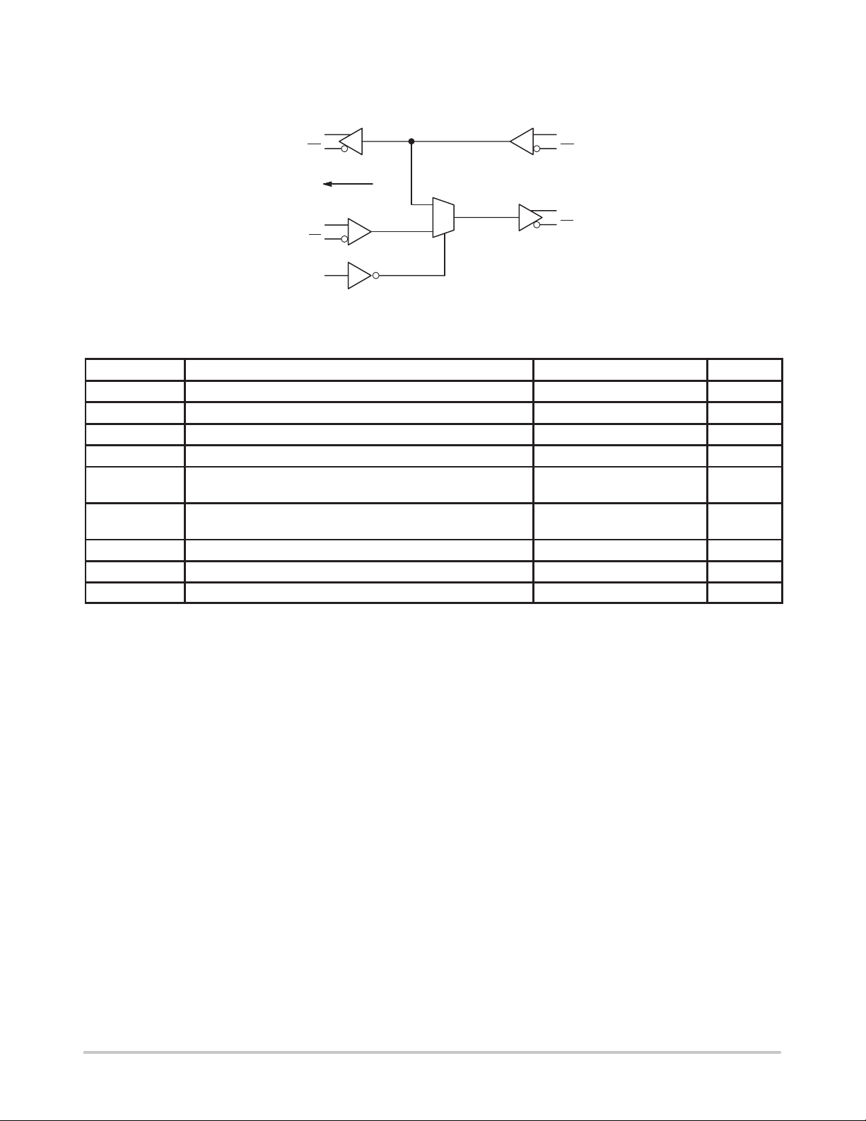
TRUTH TABLE
SEL Function
L
H
ORDERING INFORMATION
Device Package Shipping
MC10SX1 190DT TSSOP–20 75 Units/Rail
DR QT
DT QT
MC10SX1190/D
Page 2
MC10SX1190
LOGIC DIAGRAM
LOCAL
RECEIVE DATA
(ECL LEVELS)
LOCAL
TRANSMIT DATA
(ECL LEVELS)
QR
QR
V
BB
DT
DT
SEL (TTL)
DR
DR
1
0
QT
QT
ABSOLUTE MAXIMUM RATINGS*
Symbol Parameter Value Unit
V
CC
V
EE
V
IN
V
IN
I
OUT
θJA Thermal Resistance (Junction–to–Ambient) Still Air
θJC Thermal Resistance (Junction–to–Case) 30 to 35 °C/W
T
A
T
STG
* Absolute Maximum Ratings are those values beyond which damage to the device may occur. Functional operation should be restricted to
the Recommended Operating Conditions.
Power Supply Voltage (VEE = 0V) 0 to +6.0 Vdc
Power Supply Voltage (VCC = 0V) –6.0 to 0 Vdc
Input Voltage (VEE = 0V, VIN not more positive than VCC) 0 to +6.0 Vdc
Input Voltage (VCC = 0V, VIN not more negative than VEE) –6.0 to 0 Vdc
Output Current Continuous
Surge
500 LFPM
Operating Temperature Range –40 to +85 °C
Storage Temperature Range –50 to +150 °C
FROM
INPUT CABLE
(ECL LEVELS)
TO OUTPUT
CABLE
(ENHANCED SWING)
50
100
90
60
mA
°C/W
http://onsemi.com
2
Page 3
MC10SX1190
DC CHARACTERISTICS (Note 1)
-40°C 0°C 25°C 85°C
Symbol Characteristic Min Typ Max Min Typ Max Min Typ Max Min Typ Max Unit
V
V
V
V
I
CC
V
V
V
V
V
1. 10SX circuits are designed to meet the DC specifications shown in the table after thermal equilibrium has been established. The circuit is mounted in a test socket
or mounted on a printed circuit board and transverse air greater than 500lfm is maintained.
2. Values will track 1:1 with the VCC supply.
3. Outputs loaded with 50Ω to +3.0V
4. Outputs loaded with 50Ω to +2.0V
5. Outputs open circuited.
6. TTL signal threshold is 1.5V above VEE.
AC CHARACTERISTICS (Note 1 & 7)
t
PLH
t
PLH
tr,
t
f
tr,
t
f
t
skew
V
V
f
max
1. 10SX circuits are designed to meet the AC specifications shown in the table after thermal equilibrium has been established. The circuit is mounted in a test socket
or mounted on a printed circuit board and transverse air greater than 500lfm is maintained.
2. The differential propagation delay is defined as the delay from the crossing points of the differential input signals to the crossing point of the differential output
signals.
3. The single-ended propagation delay is defined as the delay from the 50% point of the input signal to the 50% point of the output signal.
4. Duty cycle skew is the difference between t
5. Minimum input swing for which AC parameters are guaranteed.
6. The CMR range is referenced to the most positive side of the differential input signal. Normal operation is obtained if the HIGH level falls within the specified range
and the peak-to-peak voltage lies between VPP
7. Data taken at V
Output Voltage High (QR,QR)
OH
OL
OH
OL
IH
IL
IH
IL
BB
VCC = 5.0V, VEE = 0V (Notes 2,3)
Output Voltage Low (QR,QR)
VCC = 5.0V, VEE = 0V (Notes 2,3)
Output Voltage High (QT,QT)
VCC = 5.0V, VEE = 0V (Notes 2,4)
Output Voltage Low (QT,QT)
VCC = 5.0V, VEE = 0V (Notes 2,4)
Quiescent Supply Current (Note 5) 55 mA
Input Voltage High (DR,DR & DT,DT)
VCC = 5.0V, VEE = 0V (Note 2)
Input Voltage Low (DR,DR & DT,DT)
VCC = 5.0V, VEE = 0V (Note 2)
Input Voltage High SEL (Note 6) 2.0 2.0 2.0 2.0 V
Input Voltage Low SEL (Note 6) 0.8 0.8 0.8 0.8 V
Output Reference Voltage
VCC = 5.0V, VEE = 0V (Note 2)
4.01 4.04 4.06 4.16 V
3.23 3.26 3.28 3.33 V
3.94 3.98 4.04 4.13 V
2.51 2.49 2.48 2.47 V
3.77 4.11 3.83 4.16 3.87 4.19 3.94 4.28 V
3.05 3.50 3.05 3.52 3.05 3.52 3.05 3.56 V
3.57 3.63 3.70 3.62 3.67 3.73 3.65 3.70 3.75 3.69 3.75 3.81 V
–40°C 0 to 85°C
Symbol Characteristic Min Typ Max Min Typ Max Unit Condition
, t
, t
Propagation Delay DR QR (Diff)
PHL
to Output (SE)
DR QT (Diff)
(SE)
DT QT (Diff)
(SE)
Propagation Delay SEL QT,QT 450 600 850 500 650 800 ps 1.5V to 50% Pt
PHL
Rise Time QR,QR
Fall Time
Rise Time QT,QT
Fall Time
240
240
425
425
425
425
118
118
230
230
ps Note 2
ps 20% to 80%
ps 20% to 80%
Note 3
80% to 20%
80% to 20%
Within Device Skew 15 15 ps Note 4
PP
CMR
Minimum Input Swing 200 200 mV Note 5
Common Mode Range 3.0 4.35 3.0 4.35 V Note 6
Maximum Operation Frequency 2.5 2.5 Gb/s
CC, nom
= 3.3V.
PLH
and t
propagation delay through a device.
PHL
and 1.0V.
Min
http://onsemi.com
3
Page 4

MC10SX1190
V
EE
R
pd
QT
QT
R
pd
V
SX1190
QR
QR
Typical value for Rpd is 160W to 260W, depending on the application. The minimum value of Rpd should not be less than 50W.
EE
V
EE
R
pd
R
pd
V
EE
Z
O
R
Z
O
Z
O
Z
O
t
R
t
Rt = Z
O
SX1190
V
TT1
R
t
R
t
V
TT1
V
TT2
R
t
R
t
V
TT2
Rt = ZO/2
QT
QT
QR
QR
Z
O
Z
O
Z
O
Z
O
Figure 2. SX1190 Termination Configuration
V
TT1
V
TT2
= VCC – 3V
= VCC – 2V
http://onsemi.com
4
Page 5

MC10SX1190
P ACKAGE DIMENSIONS
DT SUFFIX
PLASTIC PACKAGE
CASE 948E–02
ISSUE A
20X REFK
S
U0.15 (0.006) T
0.10 (0.004) V
M
S
U
T
S
K
2X
L/2
L
PIN 1
IDENT
110
1120
B
JJ1
–U–
N
S
U0.15 (0.006) T
A
K1
SECTION N–N
0.25 (0.010)
M
–V–
N
F
DETAIL E
C
G
H
DETAIL E
0.100 (0.004)
–T–
SEATING
PLANE
D
NOTES:
1. DIMENSIONING AND TOLERANCING PER ANSI
Y14.5M, 1982.
2. CONTROLLING DIMENSION: MILLIMETER.
3. DIMENSION A DOES NOT INCLUDE MOLD
FLASH, PROTRUSIONS OR GATE BURRS. MOLD
FLASH OR GATE BURRS SHALL NOT EXCEED
0.15 (0.006) PER SIDE.
4. DIMENSION B DOES NOT INCLUDE
INTERLEAD FLASH OR PROTRUSION.
INTERLEAD FLASH OR PROTRUSION SHALL NOT
EXCEED 0.25 (0.010) PER SIDE.
5. DIMENSION K DOES NOT INCLUDE DAMBAR
PROTRUSION. ALLOWABLE DAMBAR
PROTRUSION SHALL BE 0.08 (0.003) TOTAL IN
EXCESS OF THE K DIMENSION AT MAXIMUM
MATERIAL CONDITION.
6. TERMINAL NUMBERS ARE SHOWN FOR
REFERENCE ONLY.
7. DIMENSION A AND B ARE TO BE
DETERMINED AT DATUM PLANE –W–.
MILLIMETERS
–W–
DIMAMIN MAX MIN MAX
B 4.30 4.50 0.169 0.177
C 1.20 0.047
D 0.05 0.15 0.002 0.006
F 0.50 0.75 0.020 0.030
G 0.65 BSC 0.026 BSC
H 0.27 0.37 0.011 0.015
J 0.09 0.20 0.004 0.008
J1 0.09 0.16 0.004 0.006
K 0.19 0.30 0.007 0.012
K1 0.19 0.25 0.007 0.010
L 6.40 BSC 0.252 BSC
M 0 8 0 8
6.60 0.260
6.40 0.252
––– –––
____
INCHES
http://onsemi.com
5
Page 6

Notes
MC10SX1190
http://onsemi.com
6
Page 7

Notes
MC10SX1190
http://onsemi.com
7
Page 8

MC10SX1190
ON Semiconductor and are trademarks of Semiconductor Components Industries, LLC (SCILLC). SCILLC reserves the right to make changes
without further notice to any products herein. SCILLC makes no warranty , representation or guarantee regarding the suitability of its products for any particular
purpose, nor does SCILLC assume any liability arising out of the application or use of any product or circuit, and specifically disclaims any and all liability ,
including without limitation special, consequential or incidental damages. “Typical” parameters which may be provided in SCILLC data sheets and/or
specifications can and do vary in different applications and actual performance may vary over time. All operating parameters, including “Typicals” must be
validated for each customer application by customer’s technical experts. SCILLC does not convey any license under its patent rights nor the rights of others.
SCILLC products are not designed, intended, or authorized for use as components in systems intended for surgical implant into the body, or other applications
intended to support or sustain life, or for any other application in which the failure of the SCILLC product could create a situation where personal injury or
death may occur. Should Buyer purchase or use SCILLC products for any such unintended or unauthorized application, Buyer shall indemnify and hold
SCILLC and its officers, employees, subsidiaries, affiliates, and distributors harmless against all claims, costs, damages, and expenses, and reasonable
attorney fees arising out of, directly or indirectly , any claim of personal injury or death associated with such unintended or unauthorized use, even if such claim
alleges that SCILLC was negligent regarding the design or manufacture of the part. SCILLC is an Equal Opportunity/Affirmative Action Employer .
PUBLICATION ORDERING INFORMATION
North America Literature Fulfillment:
Literature Distribution Center for ON Semiconductor
P.O. Box 5163, Denver, Colorado 80217 USA
Phone: 303–675–2175 or 800–344–3860 Toll Free USA/Canada
Fax: 303–675–2176 or 800–344–3867 Toll Free USA/Canada
Email: ONlit@hibbertco.com
N. American Technical Support: 800–282–9855 Toll Free USA/Canada
EUROPE: LDC for ON Semiconductor — European Support
German Phone: 303–308–7140 (Mon–Fri 2:30pm to 5:00pm Munich Time)
German Email: ONlit–german@hibbertco.com
French Phone: 303–308–7141 (Mon–Fri 2:30pm to 5:00pm T oulouse T ime)
French Email: ONlit–french@hibbertco.com
English Phone: 303–308–7142 (Mon–Fri 1:30pm to 5:00pm UK Time)
English Email: ONlit@hibbertco.com
http://onsemi.com
ASIA/PACIFIC: LDC for ON Semiconductor — Asia Support
Phone: 303–675–2121 (T ue–Fri 9:00am to 1:00pm, Hong Kong T ime)
T oll Free from Hong Kong 800–4422–3781
Email: ONlit–asia@hibbertco.com
JAPAN: ON Semiconductor, Japan Customer Focus Center
4–32–1 Nishi–Gotanda, Shinagawa–ku, T okyo, Japan 141–8549
Phone: 81–3–5487–8345
Email: r14153@onsemi.com
Fax Response Line: 303–675–2167
800–344–3810 Toll Free USA/Canada
ON Semiconductor Website: http://onsemi.com
For additional information, please contact your local Sales Representative.
MC10SX1190/D
8
 Loading...