

Page 1
SEMICONDUCTOR TECHNICAL DATA
!
"
The MC10SX1189 is a differential receiver, differential transmitter
specifically designed to drive coaxial cables. It incorporates the output
cable drive capability of the MC10EL89 Coaxial Cable Driver with
additional circuitry to multiplex the output cable drive source between the
cable receiver or the local transmitter inputs. The multiplexer control
circuitry is TTL compatible for ease of operation.
• 425ps Propagation Delay
• 1.6V Output Swing on the Cable Driving Output
• Single +5V operation
• 75kΩ Internal Input Pull Down Resistors
• >1000 Volt ESD Protection
The MC10SX1189 is useful as a bypass element for Fibre
Channel-Arbitrated Loop (FC-AL) or Serial Storage Architecture (SSA)
applications, to create loop style interconnects with fault tolerant, active
switches at each device node. This device is particularly useful for back
panel applications where small size is desirable.
The EL89 style drive circuitry produces swings twice as large as a
standard PECL output. When driving a coaxial cable, proper termination
is required at both ends of the line to minimize reflections. The 1.6V
output swings allow for proper termination at both ends of the cable, while
maintaining the required swing at the receiving end of the cable. Because
of the larger output swings, the QT, QT
thevenin equivalent of 50Ω to VCC– 3.0V instead of 50Ω to VCC– 2.0V .
outputs are terminated into the
FIBRE CHANNEL COAXIAL
CABLE DRIVER AND LOOP
RESILIENCY CIRCUIT
16
1
D SUFFIX
PLASTIC SOIC PACKAGE
CASE 751B-05
DR DR
V
CC
1516 14 13 12 11 10
21 34567
QR QR
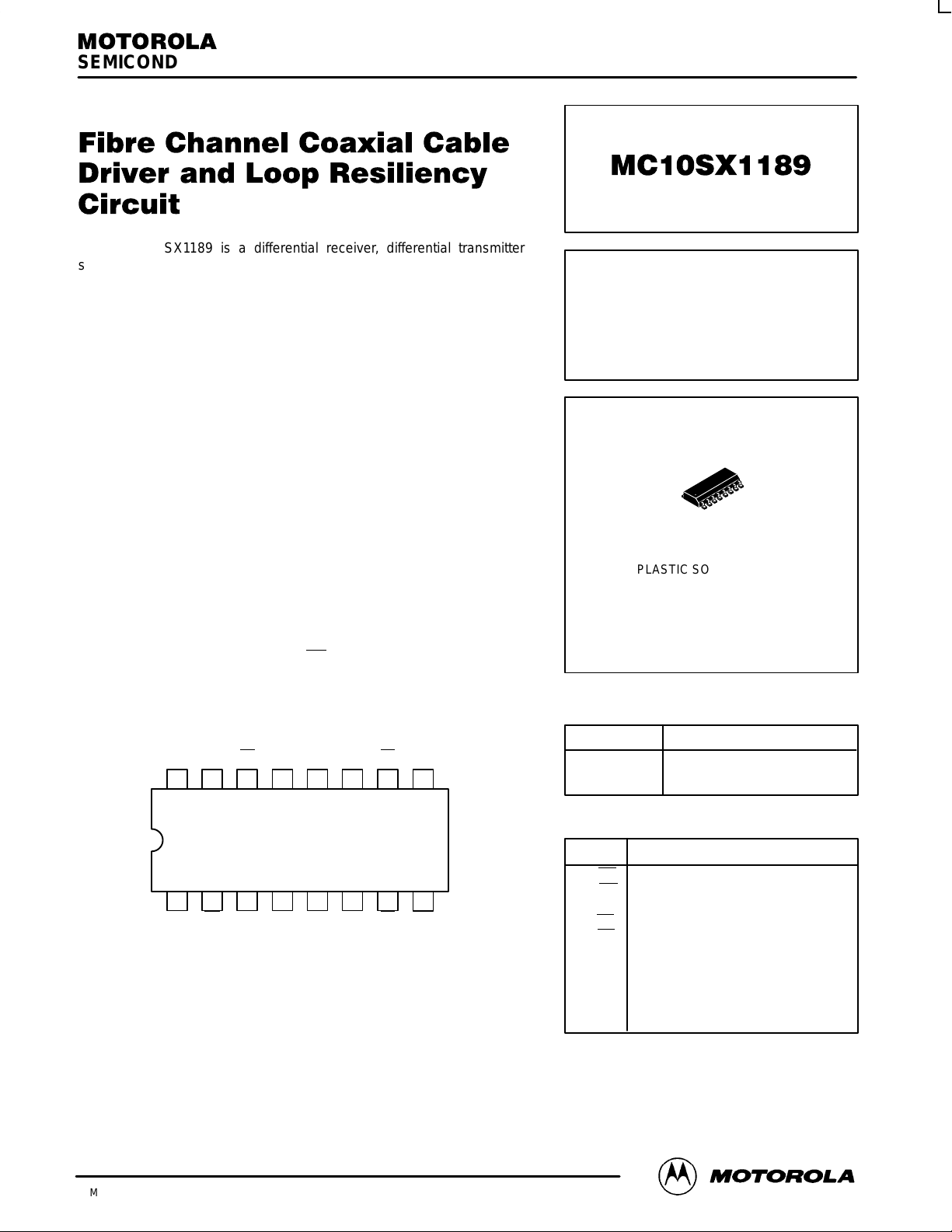
Pinout: 16-Lead SOIC (Top View)
GND VBBDT DT SEL
VCCNC VCCQT QT V
9
8
CC
TRUTH TABLE
SEL Function
L
H
PIN NAMES
Pins
DR/DR
QR/QR
DT/DT
QT/QT
SEL
V
CC
GND
V
BB
Function
Differential Input from Receive Cable
Buffered Differential Output from
Receive Cable
Differential Input to Transmit Cable
Buffered Differential Output to
Transmit Cable
Multiplexer Control Signal (TTL)
Positive Power Supply
Ground
Reference Voltage Output
DR → QT
DT → QT
3/96
Motorola, Inc. 1996
1
REV 1
Page 2
MC10SX1189
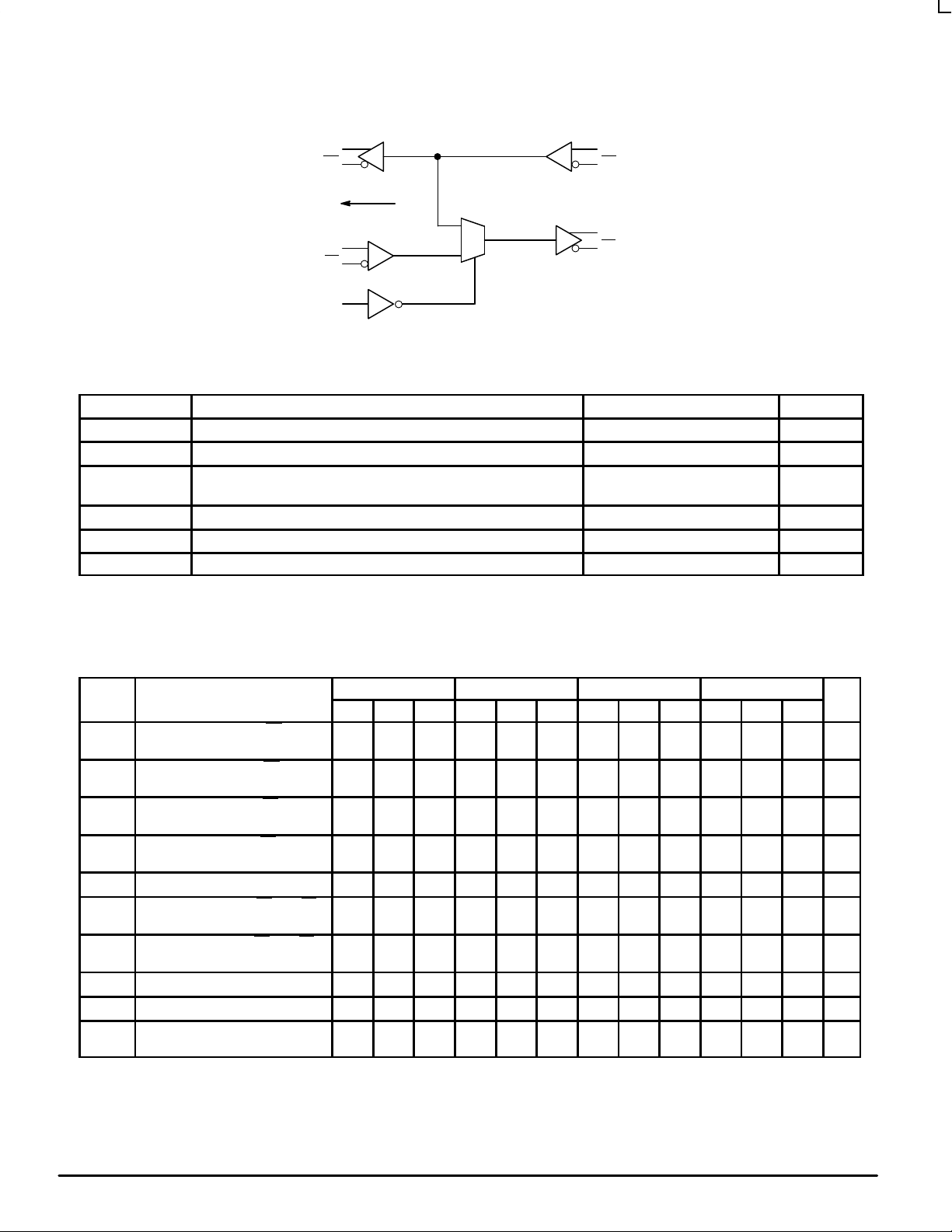
LOGIC DIAGRAM
LOCAL
RECEIVE DATA
(ECL LEVELS)
LOCAL
TRANSMIT DATA
(ECL LEVELS)
V
QR
QR
BB
DT
DT
DR
DR
1
0
QT
QT
FROM
INPUT CABLE
(ECL LEVELS)
TO OUTPUT
CABLE
(ENHANCED SWING)
SEL (TTL)
ABSOLUTE MAXIMUM RATINGS*
Symbol Parameter Value Unit
V
CC
V
IN
I
OUT
T
A
T
STG
V
CC
* Absolute Maximum Ratings are those values beyond which damage to the device may occur . Functional operation should be restricted to the
Recommended Operating Conditions.
1. Parametric values specified at 4.75 to 5.25V.
Power Supply Voltage (Referenced to GND) 0 to +7.0 Vdc
Input Voltage (Referenced to GND) 0 to +6.0 Vdc
Output Current Continuous
Surge
50
100
mA
Operating Temperature Range –40 to +85 °C
Storage Temperature Range –50 to +150 °C
Operating Voltage Range
1
4.5 to 5.5 Vdc
DC CHARACTERISTICS
Symbol Characteristic Min Typ Max Min Typ Max Min Typ Max Min Typ Max Unit
V
OH
V
OL
V
OH
V
OL
I
CC
V
IH
V
IL
V
IH
V
IL
V
BB
1. 10SX circuits are designed to meet the DC specifications shown in the table after thermal equilibrium has been established. The circuit is mounted in a test socket
or mounted on a printed circuit board and transverse air greater than 500lfm is maintained.
2. Values will track 1:1 with the VCC supply.
3. Outputs loaded with 50Ω to +3.0V
4. Outputs loaded with 50Ω to +2.0V
5. Outputs open circuited.
Output Voltage High (QR,QR)
VCC = 5.0V, GND = 0V (Notes 2,3)
Output Voltage Low (QR,QR)
VCC = 5.0V, GND = 0V (Notes 2,3)
Output Voltage High (QT,QT)
VCC = 5.0V, GND = 0V (Notes 2,4)
Output Voltage Low (QT,QT)
VCC = 5.0V, GND = 0V (Notes 2,4)
Quiescent Supply Current (Note 5) 20 25 42 22 26 47 23 27 47 25 28 47 mA
Input Voltage High (DR,DR & DT,DT)
VCC = 5.0V, GND = 0V (Note 2)
Input Voltage Low (DR,DR & DT,DT)
VCC = 5.0V, GND = 0V (Note 2)
Input Voltage High SEL 2.0 2.0 2.0 2.0 V
Input Voltage Low SEL 0.8 0.8 0.8 0.8 V
Output Reference Voltage
VCC = 5.0V, GND = 0V (Note 2)
1
-40°C 0°C 25°C 85°C
3.92 4.05 4.11 3.98 4.09 4.16 4.02 4.11 4.19 4.09 4.16 4.28 V
3.05 3.23 3.35 3.05 3.24 3.37 3.05 3.24 3.37 3.05 3.25 3.41 V
3.71 3.89 4.08 3.79 3.98 4.17 3.83 4.02 4.20 3.90 4.09 4.28 V
1.94 2.22 2.50 1.83 2.12 2.41 1.80 2.10 2.39 1.77 2.06 2.35 V
3.77 4.11 3.83 4.16 3.87 4.19 3.94 4.28 V
3.05 3.50 3.05 3.52 3.05 3.52 3.05 3.56 V
3.57 3.63 3.70 3.62 3.67 3.73 3.65 3.70 3.75 3.69 3.75 3.81 V
MOTOROLA High Performance Frequency
2
Control Products — BR1334
Page 3

MC10SX1189
AC CHARACTERISTICS1 (VCC = 4.75 to 5.25V)
–40°C 0 to 85°C
Symbol Characteristic Min Typ Max Min Typ Max Unit Condition
t
,
PLH
t
PHL
t
, t
PLH
tr,
t
f
tr,
t
f
t
skew
V
PP
V
CMR
1. 10SX circuits are designed to meet the AC specifications shown in the table after thermal equilibrium has been established. The circuit is mounted in a test socket
or mounted on a printed circuit board and transverse air greater than 500lfm is maintained.
2. The differential propagation delay is defined as the delay from the crossing points of the differential input signals to the crossing point of the differential output signals.
3. The single-ended propagation delay is defined as the delay from the 50% point of the input signal to the 50% point of the output signal.
4. Duty cycle skew is the difference between t
5. Minimum input swing for which AC parameters are guaranteed.
6. The CMR range is referenced to the most positive side of the differential input signal. Normal operation is obtained if the HIGH level falls within the specified range
and the peak-to-peak voltage lies between VPP
Propagation Delay DR → QR (Diff)
to Output (SE)
DR → QT (Diff)
(SE)
DT → QT (Diff)
(SE)
Propagation Delay SEL → QT,QT 450 600 850 500 650 800 ps 1.5V to 50% Pt
PHL
Rise Time QR,QR
Fall Time
Rise Time QT,QT
Fall Time
175
150
250
225
225
200
100
100
150
150
300
300
425
425
400
400
275
275
300
300
450
500
650
700
650
725
400
400
550
550
225
175
300
250
275
225
125
125
150
150
325
325
450
450
425
425
275
275
300
300
500
550
650
700
650
725
400
400
550
550
ps Note 2
ps 20% to 80%
ps 20% to 80%
Within Device Skew 15 15 ps Note 4
Minimum Input Swing 200 200 mV Note 5
Common Mode Range 3.00 4.35 3.00 4.35 V Note 6
PLH
and t
propagation delay through a device, Stretch input is left open.
PHL
and 1.0V.
Min
Note 3
80% to 20%
80% to 20%
Control Products — BR1334
MOTOROLAHigh Performance Frequency
3
Page 4

MC10SX1189
1
-T-
SEATING
PLANE
-A-
G
D
16 PL
0.25 (0.010) T B A
OUTLINE DIMENSIONS
D SUFFIX
PLASTIC PACKAGE
CASE 751B-05
ISSUE J
NOTES:
1. DIMENSIONING AND TOLERANCING PER ANSI
916
-B-
P 8 PL
8
0.25 (0.010) B
K
M M
R X 45°
F
C
M
M
S S
J
Y14.5M, 1982.
2. CONTROLLING DIMENSION: MILLIMETER.
3. DIMENSIONS A AND B DO NOT INCLUDE
MOLD PROTRUSION.
4. MAXIMUM MOLD PROTRUSION 0.15 (0.006)
PER SIDE.
5. DIMENSION D DOES NOT INCLUDE DAMBAR
PROTRUSION. ALLOWABLE DAMBAR
PROTRUSION SHALL BE 0.127 (0.005) TOTAL
IN EXCESS OF THE D DIMENSION AT
MAXIMUM MATERIAL CONDITION.
MILLIMETERS INCHES
MIN MINMAX MAX
DIM
A
9.80
B
3.80
C
1.35
D
0.35
F
0.40
1.27 BSC 0.050 BSC
G
J
0.19
K
0.10
M
0
°
P
5.80
R
0.25
10.00
4.00
1.75
0.49
1.25
0.25
0.25
7
6.20
0.50
°
0.386
0.150
0.054
0.014
0.016
0.008
0.004
0
°
0.229
0.010
0.393
0.157
0.068
0.019
0.049
0.009
0.009
7
°
0.244
0.019
Motorola reserves the right to make changes without further notice to any products herein. Motorola makes no warranty , representation or guarantee regarding
the suitability of its products for any particular purpose, nor does Motorola assume any liability arising out of the application or use of any product or circuit,
and specifically disclaims any and all liability, including without limitation consequential or incidental damages. “T ypical” parameters can and do vary in different
applications. All operating parameters, including “T ypicals” must be validated for each customer application by customer’s technical experts. Motorola does
not convey any license under its patent rights nor the rights of others. Motorola products are not designed, intended, or authorized for use as components in
systems intended for surgical implant into the body, or other applications intended to support or sustain life, or for any other application in which the failure of
the Motorola product could create a situation where personal injury or death may occur. Should Buyer purchase or use Motorola products for any such
unintended or unauthorized application, Buyer shall indemnify and hold Motorola and its officers, employees, subsidiaries, affiliates, and distributors harmless
against all claims, costs, damages, and expenses, and reasonable attorney fees arising out of, directly or indirectly, any claim of personal injury or death
associated with such unintended or unauthorized use, even if such claim alleges that Motorola was negligent regarding the design or manufacture of the part.
Motorola and are registered trademarks of Motorola, Inc. Motorola, Inc. is an Equal Opportunity/Affirmative Action Employer.
How to reach us:
USA/EUROPE: Motorola Literature Distribution; JAPAN: Nippon Motorola Ltd.; Tatsumi–SPD–JLDC, Toshikatsu Otsuki,
P.O. Box 20912; Phoenix, Arizona 85036. 1–800–441–2447 6F Seibu–Butsuryu–Center, 3–14–2 Tatsumi Koto–Ku, Tokyo 135, Japan. 03–3521–8315
MFAX: RMFAX0@email.sps.mot.com –TOUCHTONE (602) 244–6609 HONG KONG: Motorola Semiconductors H.K. Ltd.; 8B Tai Ping Industrial Park,
INTERNET: http://Design–NET .com 51 Ting Kok Road, Tai Po, N.T., Hong Kong. 852–26629298
MOTOROLA High Performance Frequency
4
*MC10SX1189/D*
Control Products — BR1334
◊
MC10SX1189/D
 Loading...