

Page 1
SEMICONDUCTOR TECHNICAL DATA
Order this data sheet
by MC10SX1130/D
The MC10SX1 130 is high speed LED Driver/current switch specifically
targeted for use in FDDI PMD and ANSI X3T9.3 FibreChannel 266
Mbits/s optical transmitters. The integrated circuit contains several
unique functional blocks which makes it easily configurable for use with a
variety of high performance LED devices. The part is fabricated using
Motorola’s proven MOSAIC III advanced bipolar process. The logic is
designed so that a data HIGH input results in the modulation current
flowing through the I
• Differential Data Inputs
• 300MHz Operation
• 100mA Peak Drive Current
• Extremely Low Jitter
• Duty Cycle Distortion Compensation
• Adjustable Output Current Tracking With Temperature
• Thermally Enhanced 16-Lead SOIC Package
• 75kΩ Data Input Pulldown Resistors
• +5V or –5.2V Operation
• V
Reference Available
BB
The device incorporates open collector outputs with a capability of
driving peak currents of 100mA. Since the output current switching
circuitry simply switches current between the complementary outputs, the
dynamic switching demands on the system power supply are greatly reduced. In addition, because the design is pure bipolar, the
device current drain is insensitive to the data pattern and frequency of operation.
The LED drive current is adjustable through the selection of an external set resistor, RSET. In addition, to allow for open loop
compensation for the LED’s negative optical output power tracking over temperature, a circuit is included to provide an
adjustable positive temperature tracking coefficient to the LED drive current. This is controlled through the selection of an
external resistor, RTCO.
The MC10SX1 130 incorporates novel pulse stretching circuitry which is intended to compensate for the turn-on delay and rise
and fall time asymmetry inherent in LED devices. The stretch circuitry can be used to pre-distort the input signal pulse width to
minimize the duty cycle distortion of the transmitted optical eye pattern. The stretch circuitry supports three different selections of
pre-distortion. This choice is accomplished through a unique ‘tri-state’ input which can be left open, tied to VCC, or tied to VEE to
determine the pre-distortion amount.
The device provides a VBB output for either single-ended use or as a DC bias for AC coupling the signal into the device. The
VBB pin should only be used as a bias for the MC10SX1 130 as its current sink/source capability is limited. Whenever used, the
VBB pin should be bypassed to ground via a 0.01µF capacitor.
pin to turn on the LED.
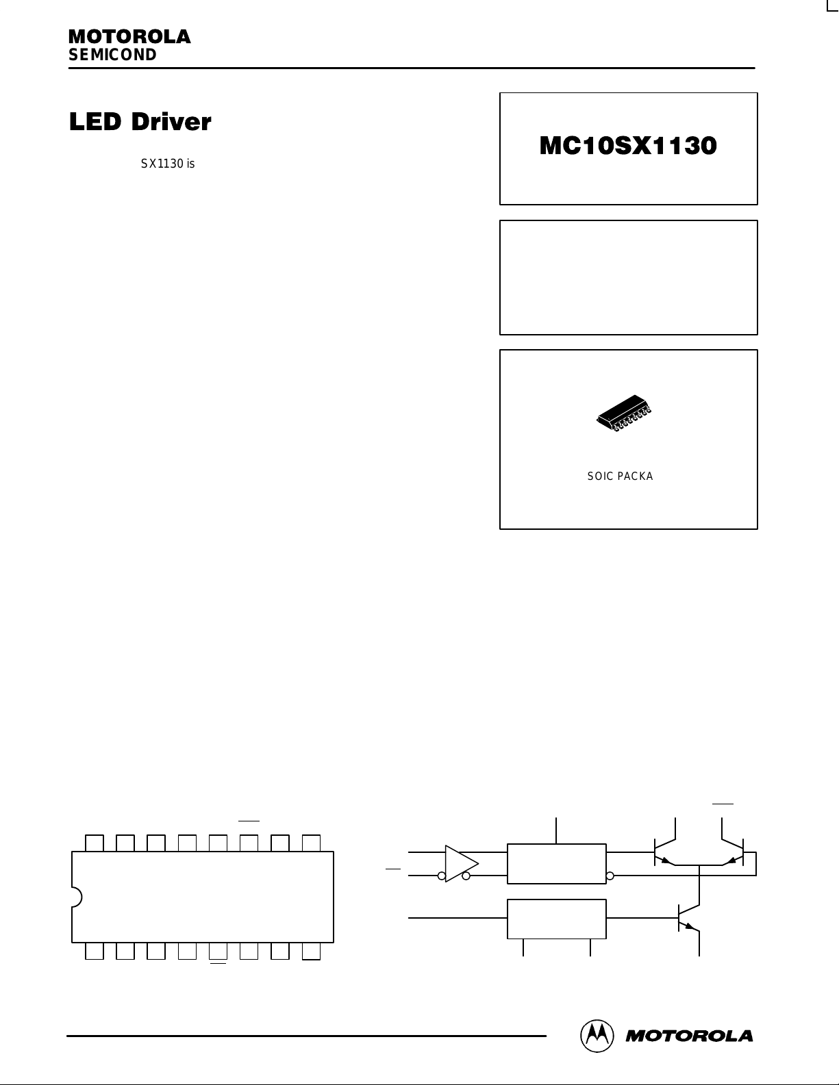
OUT
LED DRIVER
16
1
D SUFFIX
SOIC PACKAGE
CASE 751B-05
Pinout: 16-Lead Plastic Package (Top View)
Stretch VEEI
V
EE
1516 14 13 12 11 10
21 34567
VEEVCCVBBDIND
MOSAIC III is a trademark of Motorola.
3/94
OUT
RSET I
OUTVCCVEE
RTCO1RTCO2V
IN
Motorola, Inc. 1994
9
8
EE
BLOCK DIAGRAM
ECL
BUFFER
D
IN
D
IN
V
BB
Stretch
PULSE WIDTH
ADJUST CIRCUIT
BIAS
CONTROL
1
REV 1
RTCO
2
I
OUTIOUT
RSETRTCO
Page 2
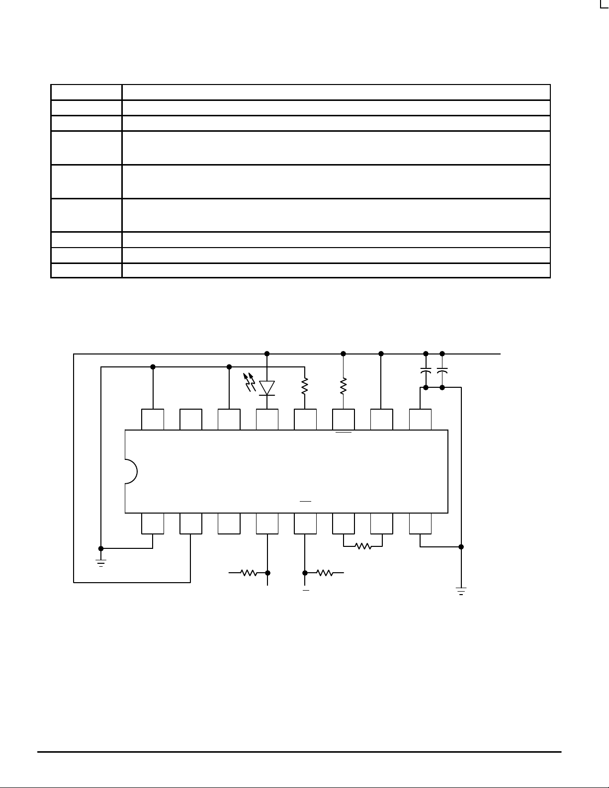
PIN FUNCTION TABLE
Pin
D
IN
I
OUT
STRETCH Control input to select the amount of duty cycle pre-distortion. When the pin is left open, no pre-distortion is introduced.
RSET Resistor to set LED drive current. This resistor sets the tail current of the output current switch and should be connected
RTCO1, RTCO
V
CC
V
EE
V
BB
Differential data inputs.
Differential open collector outputs.
If the pin is connected to VCC, the output LOW state current pulse width is increased by 155ps. When it is connected to
VEE, the current pulse width is increased by 310ps.
to the VEE plane. Since the RSET voltage compensation circuit is referenced to VEE, the RSET voltage will track 1:1 with
VEE changes, thus the voltage across the RSET resistor will remain constant.
Terminals for positive temperature tracking resistor. This resistor controls the temperature tracking rate of the voltage at
2
the RSET pin, which in turn sets the LED drive current tracking. If the two pins are shorted together, the nominal tracking
rate is 1.4mV/°C and when a 2kΩ resistor is connected across the pins, the nominal tracking rate is 4.9mV/°C.
Most positive power supply input. +5V for PECL operation or ground for standard ECL operation.
Most negative power supply input. Ground for PECL operation or –5.2V for standard ECL operation.
Reference voltage for use in single ended applications or when the input signal is AC coupled into the device.
Function
V
EE
V
EE
Stretch V
V
10
Ω
1516 14 13 12 11 10
50
I
OUT
D
IN
Ω
IN
EE
PECL
BIAS
V
BB
CC
21 34567
RSET I
D
IN
50
IN
10
Ω
OUT
RTCO1RTCO
1k
Ω
PECL
BIAS
Ω
9
V
CC
V
EE
V
2
EE
8
Figure 1. T ypical +5V Applications Circuit
SUPPLY
+5.0V
DECOUPLING
CAPACITORS
MOTOROLA High Performance Frequency
2
Control Products — BR1334
Page 3
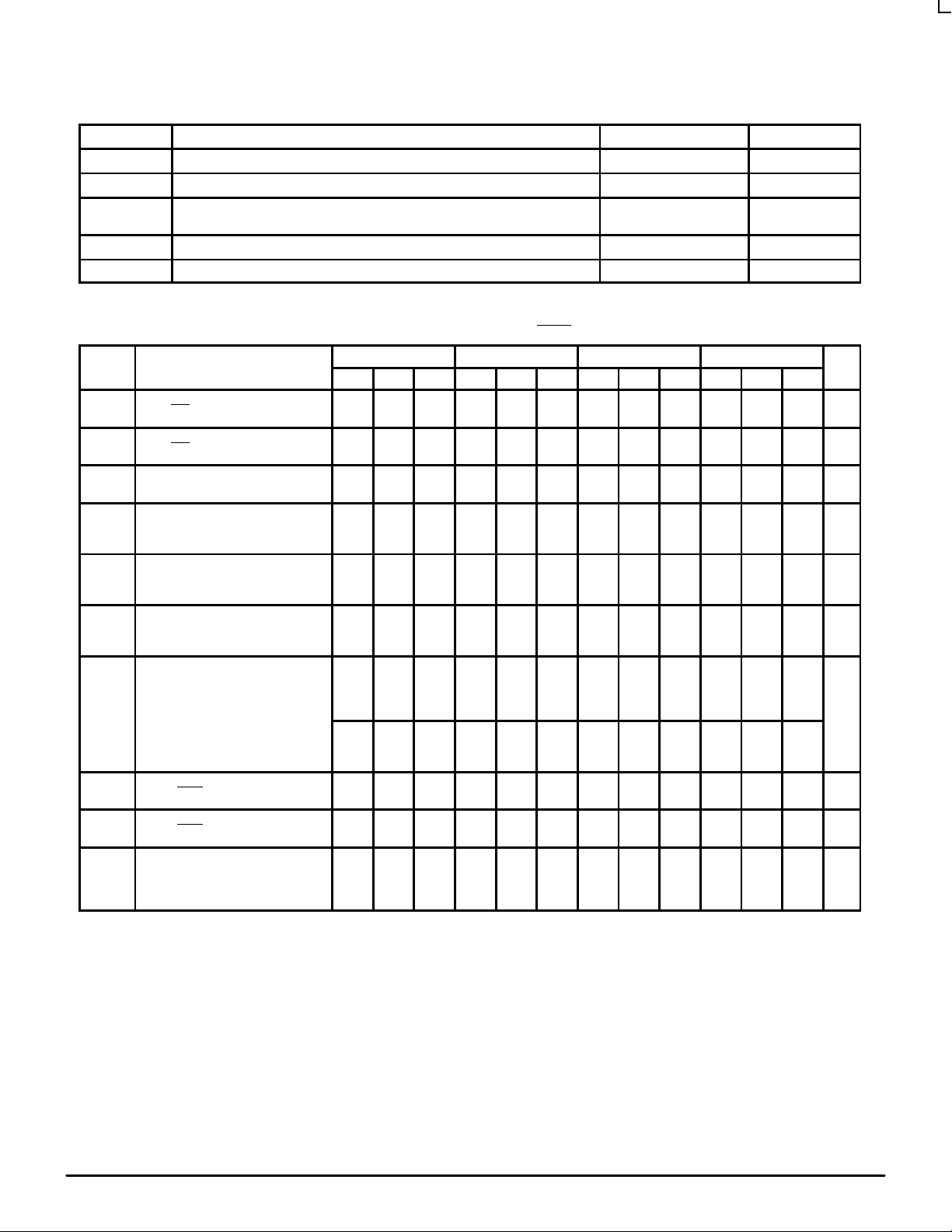
ABSOLUTE MAXIMUM RATINGS
Symbol
V
V
I
out
T
V
EE
I
A
EE
Power Supply (VCC = 0V) –7.0 to 0 VDC
Input Voltage (VCC = 0V) 0 to –6.0 VDC
Output Current Continuous
Operating Temperature Range –40 to +85 °C
Operating Range (VCC = 0) –5.5 to –4.5 VDC
*
Parameter Value Unit
Surge
* Absolute maximum rating, beyond which, device life may be impaired.
100
110
mA
DC CHARACTERISTICS1 (RTCO = 1kΩ ±5%, R
Symbol Characteristic Min Typ Max Min Typ Max Min Typ Max Min Typ Max Unit
I
IH
I
IL
I
CC
V
IH
V
IL
V
BB
V
SET
IO
IO
V
TR
1. 10SX circuits are designed to meet the DC specifications shown in the table after thermal equilibrium has been established. The circuit is mounted in a test socket
or mounted on a printed circuit board and transverse air greater than 500lfm is maintained.
2. Note that in PECL applications, VIH, VIL, VBB will vary 1:1 with the VCC supply.
3. V
4. VTR tracking measures the rate of change of the V
Input HIGH Current
(DIN, DIN
Input LOW Current
(DIN, DIN
Quiescent Supply Current
(No Load on RSET Pin)
Input HIGH Voltage
Input LOW Voltage
Output Reference Voltage
Output Voltage at RSET Pin
VCC = 5.0V, RTCO = Short
VEE = GND RTCO = 1kΩ
VCC = GND
VEE = –5.2V RTCO = 1kΩ
Output ‘ON’ Current
on
(IOUT, IOUT
Output ‘OFF’ Current
off
(IOUT, IOUT
VSET Tracking
tracks 1:1 with the VEE supply to maintain the same voltage across the RSET resistor.
SET
Pins)
Pins)
2
VCC = 5.0V, VEE = GND
VCC = GND, VEE = -4.5 to -5.5V
2
VCC = 5.0V, VEE = GND
VCC = GND, VEE = -4.5 to -5.5V
2
VCC = 5.0V, VEE = GND
VCC = GND, VEE = -4.5 to -5.5V
RTCO = 2kΩ
3
Pins)
Pins)
Short Between RTCO1 and RTCO2
1kΩ Between RTCO1 and RTCO2
2kΩ Between RTCO1 and RTCO2
RTCO = Short
RTCO = 2kΩ
4
0.5 0.5 0.5 0.5
12 17 24 12 17 24 12 18 24 12 19 24
3770
-1230
3050
-1950
3570
-1430
30 75 30 75 30 75 30 100
voltage over temperature.
SET
= R at I
SET
-40°C 0°C 25°C 85°C
200 200 200 200
4110
-890
3500
-1500
3700
-1300
600
430
230
-4400
-4570
-4770
50 50 50 50
1.4
3.4
4.9
OUT
3830
-1170
3050
-1950
3620
-1380
= R at I
635
515
355
-4365
-4485
-4645
1.4
3.4
4.9
= 10Ω ±1%, Unless Otherwise Noted)
OUT
4160
-840
3520
-1480
3730
-1270
3870
-1130
3050
-1950
3650
-1350
610
570
470
-4390
-4430
-4530
690
650
550
-4310
-4350
-4450
1.4
3.4
4.9
4190
-810
3520
-1480
3750
-1250
770
730
630
-4230
-4270
-4370
3940
-1060
3050
-1950
3690
-1310
775
855
845
-4225
-4145
-4155
1.4
3.4
4.9
µA
µA
mA
mV
4280
-720
mV
3555
-1445
mV
3810
-1190
mV
mA
µA
mV/
°C
Control Products — BR1334
MOTOROLAHigh Performance Frequency
3
Page 4

AC CHARACTERISTICS1 (RTCO = 1kΩ ±5%, R
SET
= R at I
OUT
= R at I
= 10Ω ±1%, Unless Otherwise Noted)
OUT
–40°C 0 to 85°C
Symbol Characteristic Min Typ Max Min Typ Max Unit Condition
t
,
PLH
t
PHL
t
Stretch
tr 10–90
tf 90–10
tr 20–80
tf 80–20
Jitter Jitter Square Wave Input
Propagation Delay (Differential)
to Output (Single-Ended)
Propagation Delay Stretch = OPEN
Stretch = V
Stretch = V
CC
EE
Rise Time
Fall Time
Rise Time
Fall Time
Pseudo Random Input
1300
1300
0
145
300
600
375
490
260
9
10
1000
950
120
250
510
330
360
220
1400
1400
0
155
310
880
550
600
500
6
15
1800
1850
200
380
1260
860
850
750
ns
ps Note 2
ps 10% to 90%
90% to 10%
ps 20% to 80%
80% to 20%
ps Note 3
Note 4
BW Bandwidth 300 400 300 400 MHz
t
SKEW
V
PP
V
CMR
1. 10SX circuits are designed to meet the AC specifications shown in the table after thermal equilibrium has been established. The circuit is mounted in a test socket
or mounted on a printed circuit board and transverse air greater than 500lfm is maintained.
2. When the Stretch function is used, the output low pulse width is increased by the specified amount.
3. Test condition uses a 133 MHz 50% duty cycle signal.
4. T est condition uses a 266 Mbit/s input psuedo-random data stream (n=23).
5. Duty cycle skew is the difference between t
6. Minimum input swing for which AC parameters are guaranteed.
7. The CMR range is referenced to the most positive side of the differential input signal. Normal operation is obtained if the HIGH level falls within the specified range
and the peak-to-peak voltage lies between VPP
Duty Cycle Skew (Differential) ±30 ±30 ps Note 5
Minimum Input Swing 150 150 mV Note 6
Common Mode Range –0.400 See 7 –0.400 See 7 V Note 7
PLH
and t
propagation delay through a device, Stretch input is left open.
PHL
and 1.0V. The lower end of the CMR range is dependent on VEE and is equal to VEE + 3.5V.
Min
MOTOROLA High Performance Frequency
4
Control Products — BR1334
Page 5

APPLICATIONS INFORMATION
Introduction
The MC10SX1130 is intended to be integrated into high
performance fiber optic modules or used stand-alone to drive
a packaged optical LED device. The wide frequency
response of the device allows it to be used to support a
variety of digital communication applications ranging from:
• OC1/3 SONET/SDH Links
• 100 MBit/s FDDI
• 155 MBit/s A TM
• 133/266 MBit/s FibreChannel
To support such wide ranging application areas, the LED
Driver incorporates a variety of unique features. These offer
designers added flexibility that could not previously be
realized in less integrated designs.
LED Characteristics
LED devices emit light when forward biased. The optical
power emitted by an LED is determined by the amount of
current flowing through the device. This relationship is a
relatively linear function of the current, until the device
saturates. In some ways, an LED device behaves much like a
traditional small signal silicon diode, although the forward
“ON” voltage of an LED is much larger and ranges from 1.0V
to 2.0V. In addition, for a fixed amount of current, the optical
power from the LED will decrease if the device junction
temperature increases. Another behavior of most LED
devices is that they have unequal turn-on and turn-off times.
In developing an LED transmitter, the designer must wrestle
with all these behaviors to develop a product that meets the
design targets.
LED Driver
The MC10SX1130 LED Driver accepts a digital binary
data stream which is processed by the driver circuitry to
create a current waveform to modulate the LED device. The
LED Driver contains circuitry to program the modulation
current, pre-distort the input waveform to partially
compensate for the LED turn-on/turn-off delay, and
compensate for the negative optical output power tracking
co-efficient. The LED Driver operates from a +5V supply for
PECL applications or a –5.2V supply for traditional ECL
systems. For further information on PECL, please consult
“Designing with PECL Application Note”, AN1406/D available
from a Motorola representative.
Circuit Blocks
Some of the key sub-circuits in the LED Driver are listed
below:
• Input Line Receiver
• Pulse Stretcher
• Bias Control Circuitry
• Output Current Switch
The data input circuitry has been realized as a traditional
differential ECL line receiver. It can accept either differential
100K or 10KH style ECL or PECL depending on the supply
voltage used. In addition, a VBB reference is provided for use
in single ended applications. This reference is useful if the
input signal must be AC coupled into the device.
The pulse stretcher provides two choices of duty cycle
pre-distortion. It is controlled by the input STRETCH signal.
When the pin is left open, no pre-distortion is applied to the
input waveform. If the pin is strapped to the upper or lower
rail, then the output waveform low pulse width will be
increased. In a +5V application, when the STRETCH pin is
tied to +5V, the nominal pulse width increase is 155 ps and
when it is connected to 0V, the nominal pulse width is
increased by 310 ps.
The bias control circuitry regulates the voltage supplied at
the RSET pin of the output current switch. In addition, it
implements a positive tracking circuit which provides open
loop temperature compensation for the LED’s negative
tracking coefficient. An external resistor connected between
the RTCO1 and RTCO2 is used to select the rate of voltage
change at the RSET pin.
The output current switch is the final stage in modulating
the LED. The emitter of the current source is pinned out so
that an external resistor can be used to set the modulation
current. This circuit is implemented using a fully differential
gate where both collectors are brought out. As the LED is
modulated on and off, the current switches from one collector
to another. This architecture minimizes the switching noise
inherent in some LED driver design topologies where the
modulation current is actually turned on and off.
Design Considerations
Once the user has selected an LED, the driver circuitry
should be optimized to match the characteristics of the LED.
The three circuit blocks previously described allow the user
to control the pulse width adjustment, LED drive current and
temperature tracking rate. A very simple example may best
illustrate the design process steps.
An LED has been selected which has the desired optical
output power when modulated with a waveform of 65mA. In
addition, the LED has an output power tracking coefficient of
–0.5%/°C. Thus for every 1°C rise in the case temperature of
the LED, the output power will decrease by 0.5% of the
nominal value. In addition, the LED forward voltage is 1.5V.
First, the RSET resistor must be chosen to set the desired
nominal modulation current based on the following equation:
RSET = V
The voltage at VSET is a function of the RTCO tracking
resistor, so the desired tracking rate (VTR) must also be
chosen. To determine this, the equation must be normalized
to correspond to how the LED has been specified.
Temp Co = VTR/V
The data sheet has three temperature tracking rates for
different values of the RTCO resistor. By using the V
values at 25°C and substituting those numbers into Equation
2, normalized tracking rates can be calculated.
SET/IMOD
SET
(Equation 1)
(Equation 2)
SET
Control Products — BR1334
MOTOROLAHigh Performance Frequency
5
Page 6

Normalized Tracking at 25°C
RTCO Tracking %/°C
Short +0.20
1 KΩ +0.52
A specially designed thermally enhanced leadframe has
been used to house the LED Driver. Below is a graph of the
average ΘJA plotted against air flow.
110
2 KΩ +0.89
To match the LED chosen, a 1KΩ resistor can be used.
Now that this is known, the value of the voltage at the V
SET
can be substituted into Equation 1 to determine the value of
RSET resistor which, for this example is 10Ω.
The Stretch circuit can be used to compensate for the
turn-on/turn-off delay of the LED. The circuit has been
designed for ease of use so the pin is designed to be
strapped to one of the two power plane levels to select the
pre-distortion value. If no pre-distortion is desired, the pin can
be left open. In this +5V example, the maximum amount of
pre-distortion is desired, so the STRETCH pin is connected
to ground.
In addition a resistor must be placed between I
OUT
and
VCC. In selecting this resistor, just as in the case of the
RSET, the resistor type should be chosen to dissipate the
worst case power and derated for the worst case
temperature. As a rule of thumb, the voltage drop across the
resistor should match the forward voltage across the diode.
The voltage can be larger to minimize the power dissipated
on chip when the LED is not ’ON’. Although, the voltage drop
across this resistor should not be greater than 2V. For this
example:
I
MOD(max)
R @ I
+
R @ I
= VF/I
OUT
V
SET
°
@85 C
RSET
= 1.5V/86mA = 17Ω
OUT
MOD
855mV
+
10
+
86mA
W
Because of the positive tracking circuitry in the LED driver,
the modulation current will increase over temperature. It is
important to now go back and re-calculate the numbers
under the worst case environmental conditions to ensure that
operating conditions have not been exceeded.
100
°Θ
90
( C/W)
JA
80
70
0 100 200 300 400 500
AIRFLOW (LFPM)
Figure 2. T ypical ΘJA versus Airflow
The power dissipation of the device has two components;
the quiescent power drain related to the pre-drive circuitry,
and the power dissipated in the current switch when driving
the LED.
Pd = Pstatic + Pswitching (Equation 4)
The power dissipated in the current switch is a function of
the IMOD current, the LED forward voltage, and the value of
RSET. For example in a +5V application, the following
equations can be used:
Pstatic = VCC * ICC (Equation 5)
Pswitching = (VCC-VF-V
SET
)* I
(Equation 6)
MOD
Now to calculate the dissipated power on the chip for a
nominal application.
V
= 5V
CC
V
= 1.5V
F
V
= 0.7V
SET
I
= 60mA
MOD
I
= 18mA
CC
so:
Pd = 5 * 18 + (5 - 1.5 - 0.7) * 60
Pd = 258mW
Thermal Management
LED devices tend to require large amounts of current for
most efficent operation. This requirement is then translated
into the design of the LED Driver. When large modulation
currents are required, power dissipation becomes a critical
issue and the user must be concerned about the junction
temperature of the device. The following equation can be
used to estimate the junction temperature of a device in a
given environment:
TJ = TA + PD * Θ
T
Junction Temperature
J
T
Ambient Temperature
A
P
Power Dissipation
D
Θ
Average Thermal Resistance
JA
JA
(Equation 3)
(Junction-Ambient)
MOTOROLA High Performance Frequency
6
This number can be entered into Equation 3 along with the
environmental information to calculate the nominal operating
junction temperature.
Because of the open loop feedback control in the bias
control circuitry, the revised I
value must be determined
MOD
given the tracking rate chosen so that the power dissipation
can be re-calculated. For assessing product reliability, worst
case values should be entered to calculate the maximum
junction temperature.
Reliability of Plastic Packages
Although today’s plastic packages are as reliable as
ceramic packages under most environmental conditions, as
the junction temperature increases a failure mode unique to
plastic packages becomes a significant factor in the long
term reliability of the device.
Control Products — BR1334
Page 7

Modern plastic package assembly utilizes gold wire
bonded to aluminum bonding pads throughout the
electronics industry. As the temperature of the silicon
(junction temperature) increases, an intermetallic compound
forms between the gold and aluminum interface. This
intermetallic formation results in a significant increase in the
impedance of the wire bond and can lead to performance
failure of the affected pin. With this relationship between
intermetallic formation and junction temperature established,
it is incumbent on the designer to ensure that the junction
temperature for which a device will operate is consistent with
the long term reliability goals of the system.
Reliability studies were performed at elevated ambient
temperatures (125°C) from which an arrhenius equation,
relating junction temperature to bond failure, was
established. The application of this equation yields the table
of Figure 3. This table relates the junction temperature of a
device in a plastic package to the continuous operating time
before 0.1% bond failure (1 failure per 1000 bonds)
The MC10SX1130 device is designed with chip power
levels that permit acceptable reliability levels, in most
systems, under the conventional 500 lfpm (2.5m/s) airflow.
T = 6.376 × 10⁻⁹ e
11554.267
273.15 + T
J
Where:
T = Time to 0.1% bond failure
Junction
Temp. (°C)
80 1,032,200 117.8
90 419,300 47.9
100 178,700 20.4
110 79,600 9.1
120 37,000 4.2
130 17,800 2.0
140 8,900 1.0
Time (Hrs.) Time (yrs.)
Figure 3. Tj vs Time to 0.1% Bond Failure
Control Products — BR1334
MOTOROLAHigh Performance Frequency
7
Page 8

-T-
SEATING
PLANE
OUTLINE DIMENSIONS
D SUFFIX
PLASTIC SOIC PACKAGE
-A-
CASE 751B-05
916
-B-
8 PL
P
1
8
0.25 (0.010) B
M M
G
K
R X 45°
F
C
J
D
16 PL
0.25 (0.010) T B A
M
M
S S
NOTES:
1. DIMENSIONING AND TOLERANCING PER ANSI
Y14.5M, 1982.
2. CONTROLLING DIMENSION: MILLIMETER.
3. DIMENSION A AND B DO NOT INCLUDE MOLD
PROTRUSION.
4. MAXIMUM MOLD PROTRUSION 0.15 (0.006)
PER SIDE.
5. DIMENSION D DOES NOT INCLUDE DAMBAR
PROTRUSION. ALLOWABLE DAMBAR
PROTRUSION SHALL BE 0.127 (0.005) TOTAL
IN EXCESS OF THE D DIMENSION AT
MAXIMUM MATERIAL CONDITION.
MILLIMETERS INCHES
MIN MINMAX MAX
DIM
A
9.80
B
3.80
C
1.35
D
0.35
F
0.40
1.27 BSC 0.050 BSC
G
J
0.19
K
0.10
M
°
0
P
5.80
R
0.25
10.00
4.00
1.75
0.49
1.25
0.25
0.25
7
6.20
0.50
0.386
0.393
0.150
0.157
0.054
0.068
0.014
0.019
0.016
0.049
0.008
0.009
0.004
0.009
°
°
0
0.229
0.010
7
0.244
0.019
°
Motorola reserves the right to make changes without further notice to any products herein. Motorola makes no warranty , representation or guarantee regarding
the suitability of its products for any particular purpose, nor does Motorola assume any liability arising out of the application or use of any product or circuit,
and specifically disclaims any and all liability, including without limitation consequential or incidental damages. “Typical” parameters can and do vary in different
applications. All operating parameters, including “T ypicals” must be validated for each customer application by customer’s technical experts. Motorola does
not convey any license under its patent rights nor the rights of others. Motorola products are not designed, intended, or authorized for use as components in
systems intended for surgical implant into the body, or other applications intended to support or sustain life, or for any other application in which the failure of
the Motorola product could create a situation where personal injury or death may occur. Should Buyer purchase or use Motorola products for any such
unintended or unauthorized application, Buyer shall indemnify and hold Motorola and its officers, employees, subsidiaries, affiliates, and distributors harmless
against all claims, costs, damages, and expenses, and reasonable attorney fees arising out of, directly or indirectly, any claim of personal injury or death
associated with such unintended or unauthorized use, even if such claim alleges that Motorola was negligent regarding the design or manufacture of the part.
Motorola and are registered trademarks of Motorola, Inc. Motorola, Inc. is an Equal Opportunity/Affirmative Action Employer.
Literature Distribution Centers:
USA: Motorola Literature Distribution; P.O. Box 20912; Phoenix, Arizona 85036.
EUROPE: Motorola Ltd.; European Literature Centre; 88 T anners Drive, Blakelands, Milton Keynes, MK14 5BP, England.
JAPAN: Nippon Motorola Ltd.; 4-32-1, Nishi-Gotanda, Shinagawa-ku, Tokyo 141 Japan.
ASIA-PACIFIC: Motorola Semiconductors H.K. Ltd.; Silicon Harbour Center, No. 2 Dai King Street, Tai Po Industrial Estate, Tai Po, N.T., Hong Kong.
3PHX32168-1 PRINTED IN USA 3/94 IMPERIAL LITHO XXXXX 7,500 LOGIC YDAAAA
MOTOROLA High Performance Frequency
8
◊
*MC10SX1130/D*
Control Products — BR1334
MC10SX1130/D
 Loading...