

Page 1
SEMICONDUCTOR TECHNICAL DATA
2–121
REV 5
Motorola, Inc. 1996
3/93
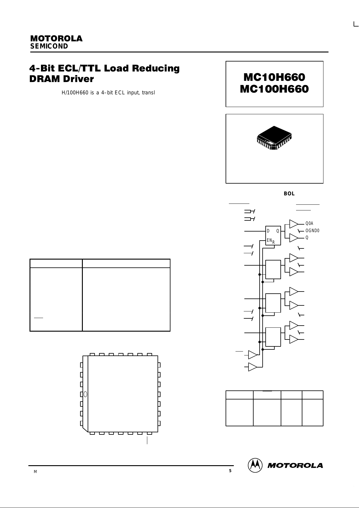
The MC10H/100H660 is a 4–bit ECL input, translating DRAM address
driver, ideally suited for driving TTL compatible DRAM inputs from an ECL
system. It is designed for use in high capacity, highly interleaved DRAM
memory boards, that directly interface to a high speed, pipelined ECL bus
interface, where new operations may be initiated to the board at up to a 50
MHz rate.
The latch provides the capability for the memory controller to propagate
new addresses to different banks without having to wait for the address timing
constraints to be satisfied from a previous memory operation. The dual output
fanout reduces input loading from the controller by a factor of two, thus
significantly improving board etch propagation delays from the controller,
without the need for additional ECL buffering.
The H660 features special TTL outputs which do not have an IOS limiting
resistor, therefore allowing rapid charging of the load capacitance. Output
voltage levels are designed specifically for driving DRAM inputs. The output
stages feature separate power and ground pins to isolate output switching
noise from internal circuitry, and also to improve simultaneous switching
performance.
The 10H version is compatible with MECL 10H ECL logic levels. The
100H version is compatible with 100K levels.
• High Capacitive Drive Outputs to Drive DRAM Address Inputs
• Extra TTL and ECL Power/Ground Pins to Minimize Switching Noise
• Dual Supply
• 10.7 ns Max. D to Q into 300 pF
PIN NAMES
PIN FUNCTION
OGND[0:3] Output Ground (0V)
OVT01, OVT23 Output VCCT (+5.0 V)
IGND01, IGND23 Internal TTL Ground (OV)
IVT01, IVT23 Internal TTL VCCT (+5.0 V)
VEE ECL Neg. Supply (–5.2/ –4.5 V)
VCCE ECL Ground (0V)
D[0:3] Data Inputs (ECL)
Q[0:3]A, Q[0:3]B Data Outputs (TTL levels)
LEN Latch Enable (ECL)
R Reset (ECL)
Q2A
OGND2
Q2B
OVT23
Q3A
OGND3
Q3B
IVT01
IGND01
VEE
VEE
D0
LEN
D1
1
567891011
25 24 23 22 21 20 19
Pinout: 28–Lead PLCC
(Top View)
26
27
28
2
3
412
13
14
15
16
17
18Q1B
OGND1
Q1A
OVT01
Q0B
OGND0
Q0A
IVT23
IGND23
VCCE
VCCE
D3
D2
R
FN SUFFIX
PLASTIC PACKAGE
CASE 776–02
EN
LOGIC SYMBOL
D
EN
R
Q
Q0A
OGND0
Q0B
D
Q1A
OGND1
Q1B
R
Q
D
EN
R
Q
Q2A
OGND2
Q2B
D
EN
R
Q
Q3A
OGND3
Q3B
IGND01
IVT01
IVT23
IGND23
OVT01
ECL Inputs
DRAM Driver
Outputs
VEE
VCCE
D0
D1
D2
D3
LEN
R
OVT23
D
L
H
X
X
LEN
H
H
L
X
R
L
L
L
H
Q
L
H
Q
0
L
TRUTH TABLE
Page 2
MC10H660 MC100H660
MOTOROLA MECL Data
DL122 — Rev 6
2–122
DC CHARACTERISTICS: V
CCT
= 5.0 V ± 10%; VEE = –5.2 V ±5% (10H version); VEE = –4.2 V to –5.5 V (100H version)
0°C 25°C 85°C
Symbol Characteristic min max min max min max Unit Condition
I
EE
Power Supply Current
ECL 41.8 44.0 46.2 mA
I
CCH
TTL
77.0 77.1 79.2 mA
I
CCL
94.6 95.7 96.8 mA
TTL CHARACTERISTICS: V
CCT
= 5.0 V ± 10%; VEE = –5.2 V ±5% (10H version); VEE = –4.2 V to –5.5 V (100H version)
0°C 25°C 85°C
Symbol Characteristic min max min max min max Unit Condition
V
OH
Output HIGH Voltage 2.6 2.6 2.6 V IOH = –24 mA
V
OL
Output LOW Voltage 0.50 0.50 0.50 V IOL = 24 mA
I
OS
Output Short Circuit Current* * * * V See Note 1
1. The outputs must not be shorted to ground, as this will result in permanent damage to the device. The high drive outputs of this device do not
include a limiting IOS resistor. Minimum recommended load capacitance is 100 pF. Precise output performance and waveforms will depend
on the exact nature of the actual load. The lumped load is of course an approximation to a real memory system load.
AC Characteristics: V
CCT
= 5.0 V ± 10%; VEE = –5.2 V ±5% (10H version) VEE = –4.2 V to –5.5 V (100H version)
0°C 25°C 85°C
Symbol Characteristic min max min max min max Unit Condition
t
s
Set–up Time, D to LEN 0.5 0.5 0.5 ns
t
n
Hold Time, D to LEN 1.5 1.5 1.5 ns
tw(H) LEN Pulse Width, HIGH 2.0 2.0 2.0 ns
t
R
t
F
Output Rise/Fall Time
0.8 V – 2.0 V
0.5 2.0 0.5 2.0 0.5 2.0 ns CL = 200 pF
t
PLH
t
PHL
Propagation Delay
to Output
D 3.0
4.0
4.5
6.0
8.0
9.5
3.0
4.0
4.5
6.0
8.0
9.5
3.0
4.0
4.5
6.0
8.0
9.5
ns CL = 100 pF
CL = 200 pF
CL = 300 pF
50% point of ECL input
to 1.5 V point of TTL
output
LEN 4.3
4.9
5.4
6.9
8.9
10.4
4.3
4.9
5.4
6.9
8.9
10.4
4.3
4.9
5.4
6.9
8.9
10.4
ns CL = 100 pF
CL = 200 pF
CL = 300 pF
t
PHL
Propagation Delay
to Output
R 4.1
4.5
5.0
9.1
8.5
10.0
4.1
4.5
5.0
9.1
8.5
10.0
4.1
4.5
5.0
9.1
8.5
10.0
ns CL = 100 pF
CL = 200 pF
CL = 300 pF
t
PLH
Propagation Delay
to Output
D 3.9
4.8
5.8
5.9
7.2
8.8
3.9
4.8
5.8
5.9
7.2
8.8
4.0
5.0
5.9
6.1
7.4
8.9
ns CL = 100 pF
CL = 200 pF
CL = 300 pF
50% point of ECL input
to 2.4 V point of TTL
output
LEN 4.7
5.5
6.3
7.1
8.3
9.5
4.7
5.5
6.3
7.1
8.3
9.5
4.8
5.6
6.4
7.2
8.4
9.6
ns CL = 100 pF
CL = 200 pF
CL = 300 pF
t
PHL
Propagation Delay
to Output
D 4.5
6.0
7.0
6.7
9.0
10.6
4.5
6.0
7.0
6.7
9.0
10.6
4.4
6.0
6.9
6.6
9.0
10.3
ns CL = 100 pF
CL = 200 pF
CL = 300 pF
50% point of ECL input
to 0.8 V point of TTL
output
LEN 4.0
4.9
6.0
6.0
7.3
9.0
4.0
4.9
6.0
6.0
7.3
9.0
4.0
4.9
5.9
6.0
7.3
8.9
ns CL = 100 pF
CL = 200 pF
CL = 300 pF
R 4.3
6.1
7.2
6.5
9.1
10.8
4.3
6.1
7.2
6.5
9.1
10.8
4.3
6.1
7.2
6.5
9.1
10.8
ns CL = 100 pF
CL = 200 pF
CL = 300 pF
Page 3
MC10H660 MC100H660
2–123 MOTOROLAMECL Data
DL122 — Rev 6
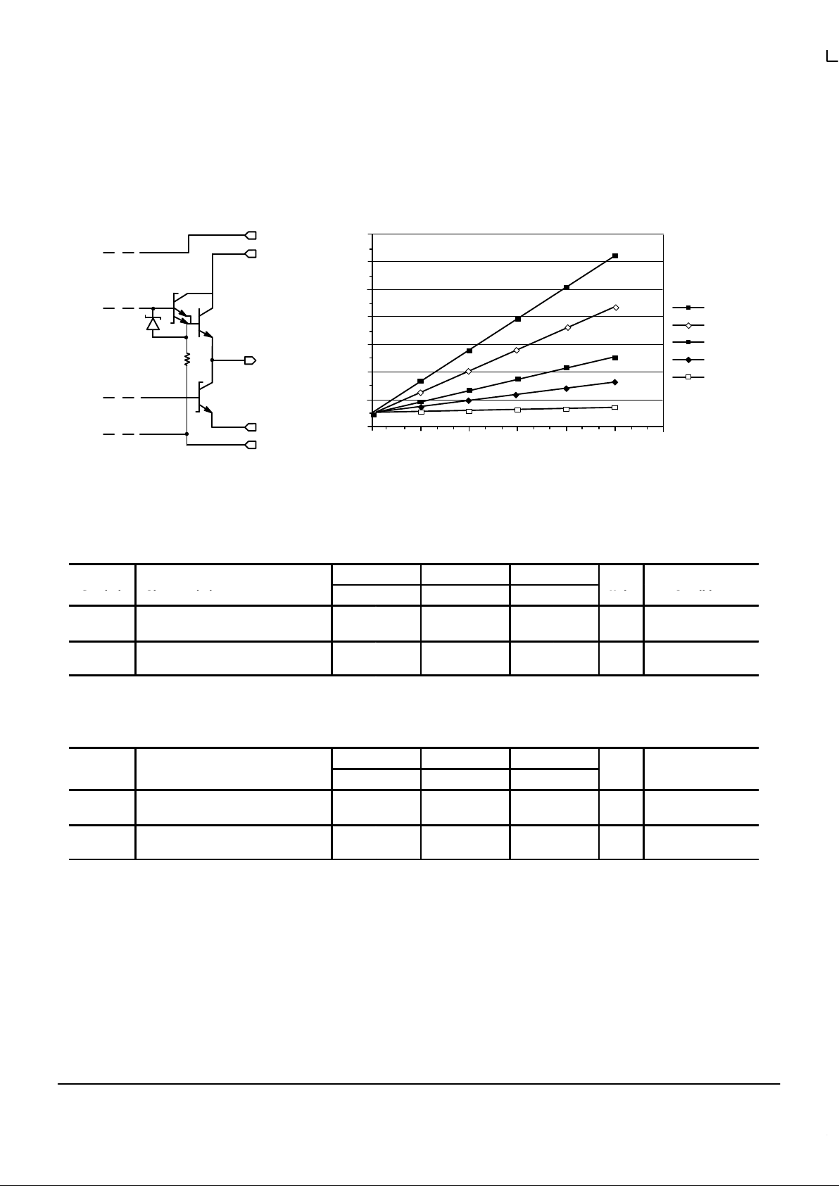
– Output Q0A Structure Shown – typical
INTERNAL TTL GROUND IGND01
OGND0
Q0A
OVT01
IVT01
INTERNAL TTL POWER
POWER VS FREQUENCY
PER BIT
FREQUENCY,
MHZ
P
TOTAL
= P
STATIC
+ P
DYNAMIC
P
DYNAMIC
= CL
ƒ
V
SWING VCC
120100806040200
0
100
200
300
400
500
600
700
Power, mW
300 PF
200 PF
100 PF
50 PF
NO LOAD
OUTPUT STRUCTURE POWER VS FREQUENCY
10H ECL DC Characteristics:
V
CCT
= 5.0 V ± 10%; VEE = –5.2 V ± 5%
0°C 25°C 85°C
Symbol Characteristic
min max min max min max
Unit Condition
I
IH
I
IL
Input HIGH Current
Input LOW Current
1.5
225
1.0
145
1.0
145 µA
µA
V
IH
V
IL
Input HIGH Voltage
Input LOW Voltage
–1170
–1950
–840
–1480
–1130
–1950
–810
–1480
–1060
–1950
–720
–1445mVmV
100H ECL DC Characteristics: V
CCT
= 5.0 V ± 10%; VEE = –4.2 V to –5.5 V
0°C 25°C 85°C
Symbol Characteristic
min max min max min max
Unit Condition
I
IH
I
IL
Input HIGH Current
Input LOW Current
1.5
225
1.0
145
1.0
145 µA
µA
V
IH
V
IL
Input HIGH Voltage
Input LOW Voltage
–1165
–1810
–880
–1475
–1165
–1810
–880
–1475
–1165
–1810
–880
–1475mVmV
Page 4

MC10H660 MC100H660
MOTOROLA MECL Data
DL122 — Rev 6
2–124
AC TEST SET–UP
CL = 100 pF
PULSE
GEN.
100 PF
50
Ω
B
50
Ω
A
450
Ω
D.U.T.
SCOPE
The MC10H/100 H660 ECL–TTL DRAM Address Driver
The MC 10H/100H660 was designed for use in high capacity,
highly interleaved DRAM memory boards, that directly interface
to a high speed, pipelined ECL bus interface, where new
operations may be initiated to the board at a 50 MHz rate ( e.g.
bipolar RISC systems).
The following briefly discusses the major design features of
the part over existing semiconductor devices traditionally
used in interfacing DRAMs in high performance system
environments.
1. ECL Translator
High performance memory systems of the past that were
interfaced to ECL buses had to rely on separate ECL
translators and DRAM drivers to interface to large DRAM
arrays, which is acceptable if the module is not highly
interleaved and the bus cycle time is comparable to the DRAM
access time. This becomes inadequate as the cycle time of the
interface becomes significantly faster than the address timing
requirements of the RAM, and as the degree of internal board
interleaving increases. These higher performance demands
require that the internal address and control signals
propagated to the DRAM drivers be implemented in ECL, thus
requiring the integration of the driver and translator functions.
Integration of the translator/drive function also reduces
access latency, as well as keeping DRAM timing parameters
from being violated, due to the excessive delays encountered
with separate parts.
2. MOS Drive Capacity
Outputs are specifically designed for driving large numbers
of DRAMs ([300 pF), which reduce the number of parts and
power requirements needed per board. Output voltage levels
are designed specifically for driving DRAM inputs. No ECL
translator parts on the market today provide the designer with
this drive capability as well as the flexibility to vary the number
of DRAMs that are driven by the part.
3. Transparent Latch
The latch is added to provide the capability for a memory
controller to propagate new addresses to different banks
without having to wait for the address timing constraints to be
satisfied from a previous memory operation. For system
implementations where this is acceptable, the user has the
capability to keep the latch open, thus having the part act as
an address translator/buffer, with minimal performance impact
due to the additional propagation delay incurred from the
internal latch. The latch is controlled within an already existing
DRAM timing signal.
4. 1:2 Output Fanout
This function is useful in that it reduces input loading from
the controller by a factor of two, thus significantly improving
board etch propagation delays from the controller to the large
number of translators, without the addition of ECL glue logic
parts to reduce the loading. In large memory boards, so many
translators are needed that this type of organization is not a
handicap.
5. Low Skew, Low Propagation Delay
Low skew of the part as well as fast propagation delay
enable faster overall DRAM operation to be attained than is
possible with existing parts.
6. Power and Package Pin Layout
The H660 is specifically designed with additional power and
ground pins to greatly improve simultaneous switching
performance over existing driver parts.
Page 5

MC10H660 MC100H660
2–125 MOTOROLAMECL Data
DL122 — Rev 6
0255075
VOLTAGE
TIME
CL = 300pF
RS = 8
Ω
OUTPUT WAVEFORMS
simulated
Example 1
. An output load consisting of just CL = 50 pF results in
overshoot at the output Q:
Example 2
. In a memory system application, use of an external
source resistor is suggested. Simulations run with RS = 8Ω and
CL = 300pF leads to clean waveforms both at the output, Q, and
at point Qp:
QP
Q
H660 OUTPUT
0255075
VOLTAGE
TIME
–2
2
Q
D
D
QP
Q
4
6
8
0
8
6
4
2
0
–2
Page 6

MC10H660 MC100H660
MOTOROLA MECL Data
DL122 — Rev 6
2–126
OUTLINE DIMENSIONS
FN SUFFIX
PLASTIC PLCC PACKAGE
CASE 776–02
ISSUE D
NOTES:
1. DATUMS –L–, –M–, AND –N– DETERMINED
WHERE TOP OF LEAD SHOULDER EXITS
PLASTIC BODY AT MOLD PARTING LINE.
2. DIMENSION G1, TRUE POSITION TO BE
MEASURED AT DATUM –T–, SEATING PLANE.
3. DIMENSIONS R AND U DO NOT INCLUDE
MOLD FLASH. ALLOWABLE MOLD FLASH IS
0.010 (0.250) PER SIDE.
4. DIMENSIONING AND TOLERANCING PER
ANSI Y14.5M, 1982.
5. CONTROLLING DIMENSION: INCH.
6. THE PACKAGE TOP MAY BE SMALLER THAN
THE PACKAGE BOTTOM BY UP TO 0.012
(0.300). DIMENSIONS R AND U ARE
DETERMINED AT THE OUTERMOST
EXTREMES OF THE PLASTIC BODY
EXCLUSIVE OF MOLD FLASH, TIE BAR
BURRS, GATE BURRS AND INTERLEAD
FLASH, BUT INCLUDING ANY MISMATCH
BETWEEN THE TOP AND BOTTOM OF THE
PLASTIC BODY.
7. DIMENSION H DOES NOT INCLUDE DAMBAR
PROTRUSION OR INTRUSION. THE DAMBAR
PROTRUSION(S) SHALL NOT CAUSE THE H
DIMENSION TO BE GREATER THAN 0.037
(0.940). THE DAMBAR INTRUSION(S) SHALL
NOT CAUSE THE H DIMENSION TO BE
SMALLER THAN 0.025 (0.635).
–N–
–M–
–L–
V
W
D
D
Y BRK
28 1
VIEW S
S
L–M
S
0.010 (0.250) N
S
T
S
L–M
M
0.007 (0.180) N
S
T
0.004 (0.100)
G1
G
J
C
Z
R
E
A
SEATING
PLANE
S
L–M
M
0.007 (0.180) N
S
T
–T–
B
S
L–M
S
0.010 (0.250) N
S
T
S
L–M
M
0.007 (0.180) N
S
T
U
S
L–M
M
0.007 (0.180) N
S
T
Z
G1X
VIEW D–D
S
L–M
M
0.007 (0.180) N
S
T
K1
VIEW S
H
K
F
S
L–M
M
0.007 (0.180) N
S
T
DIM MIN MAX MIN MAX
MILLIMETERSINCHES
A 0.485 0.495 12.32 12.57
B 0.485 0.495 12.32 12.57
C 0.165 0.180 4.20 4.57
E 0.090 0.110 2.29 2.79
F 0.013 0.019 0.33 0.48
G 0.050 BSC 1.27 BSC
H 0.026 0.032 0.66 0.81
J 0.020 ––– 0.51 –––
K 0.025 ––– 0.64 –––
R 0.450 0.456 11.43 11.58
U 0.450 0.456 11.43 11.58
V 0.042 0.048 1.07 1.21
W 0.042 0.048 1.07 1.21
X 0.042 0.056 1.07 1.42
Y ––– 0.020 ––– 0.50
Z 2 10 2 10
G1 0.410 0.430 10.42 10.92
K1 0.040 ––– 1.02 –––
____
Page 7

MC10H660 MC100H660
2–127 MOTOROLAMECL Data
DL122 — Rev 6
Motorola reserves the right to make changes without further notice to any products herein. Motorola makes no warranty , representation or guarantee regarding
the suitability of its products for any particular purpose, nor does Motorola assume any liability arising out of the application or use of any product or circuit, and
specifically disclaims any and all liability, including without limitation consequential or incidental damages. “T ypical” parameters which may be provided in Motorola
data sheets and/or specifications can and do vary in different applications and actual performance may vary over time. All operating parameters, including “Typicals”
must be validated for each customer application by customer’s technical experts. Motorola does not convey any license under its patent rights nor the rights of
others. Motorola products are not designed, intended, or authorized for use as components in systems intended for surgical implant into the body, or other
applications intended to support or sustain life, or for any other application in which the failure of the Motorola product could create a situation where personal injury
or death may occur. Should Buyer purchase or use Motorola products for any such unintended or unauthorized application, Buyer shall indemnify and hold Motorola
and its officers, employees, subsidiaries, affiliates, and distributors harmless against all claims, costs, damages, and expenses, and reasonable attorney fees
arising out of, directly or indirectly, any claim of personal injury or death associated with such unintended or unauthorized use, even if such claim alleges that
Motorola was negligent regarding the design or manufacture of the part. Motorola and are registered trademarks of Motorola, Inc. Motorola, Inc. is an Equal
Opportunity/Affirmative Action Employer.
How to reach us:
USA/EUROPE/Locations Not Listed: Motorola Literature Distribution; JAPAN: Nippon Motorola Ltd.; Tatsumi–SPD–JLDC, 6F Seibu–Butsuryu–Center,
P.O. Box 20912; Phoenix, Arizona 85036. 1–800–441–2447 or 602–303–5454 3–14–2 Tatsumi Koto–Ku, Tokyo 135, Japan. 03–81–3521–8315
MFAX: RMF AX0@email.sps.mot.com – T OUCHTONE 602–244–6609 ASIA/PACIFIC: Motorola Semiconductors H.K. Ltd.; 8B Tai Ping Industrial Park,
INTERNET: http://Design–NET.com 51 Ting Kok Road, Tai Po, N.T., Hong Kong. 852–26629298
MC10H660/D
*MC10H660/D*
◊
 Loading...