

Page 1
MOTOROLA
SEMICONDUCTOR TECHNICAL DATA
PECL/TTL-TTL 1:8 Clock
Distribution Chip
The MC10H/100H646 is a single supply , low skew translating 1:8 clock
driver. Devices in the Motorola H600 translator series utilize the 28–lead
PLCC for optimal power pinning, signal flow through and electrical
performance. The single supply H646 is similar to the H643, which is a
dual supply 1:8 version of the same function.
MC10H646
MC100H646
PENTIUM
MICROPROCESSOR
• PECL/TTL–TTL Version of Popular ECLinPS E111
• Low Skew
• Guaranteed Skew Spec
• Tri–State Enable
• Differential Internal Design
• V
Output
BB
• Single Supply
• Extra TTL and ECL Power/Ground Pins
• Matched High and Low Output Impedance
• Meets Specifications Required to Drive the Pentium Microprocessor
The H646 was designed specifically to drive series terminated
transmission lines. Special techniques were used to match the HIGH and
LOW output impedances to about 7ohms. This simplifies the choice of the
termination resistor for series terminated applications. T o match the HIGH
and LOW output impedances, it was necessary to remove the standard
IOS limiting resistor. As a result, the user should take care in preventing an
output short to ground as the part will be permanently damaged.
The H646 device meets all of the requirements for driving the 60 and 66MHz Pentium Microprocessor. The device has no PLL
components, which greatly simplifies its implementation into a digital design. The eight copies of the clock allows for
point–to–point clock distribution to simplify board layout and optimize signal integrity.
The H646 provides differential PECL inputs for picking up LOW skew PECL clocks from the backplane and distributing it to
TTL loads on a daughter board. When used in conjunction with the MC10/100E1 11, very low skew, very wide clock trees can be
designed. In addition, a TTL level clock input is provided for flexibility. Note that only one of the inputs can be used on a s ingle
chip. For correct operation, the unused input pins should be left open.
The Output Enable pin forces the outputs into a high impedance state when a logic 0 is applied.
The output buffers of the H646 can drive two series terminated, 50Ω transmission lines each. This capability allows the H646
to drive up to 16 different point–to–point clock loads. Refer to the Applications section for a more detailed discussion in this area.
The 10H version is compatible with MECL 10H ECL logic levels. The 100H version is compatible with 100K levels.
PECL/TTL–TTL
CLOCK DRIVER
FN SUFFIX
PLASTIC PACKAGE
CASE 776–02
MECL 10H and ECLinPS are trademarks of Motorola, Inc. Pentium is a trademark of Intel Corporation.
8/94
Motorola, Inc. 1996
1
REV 1
Page 2
Q3
OGND
Q2
OVT
Q1
OGND
Q0
Q4
OGNDQ5
25 24 23 22 21 20 19
26
27
28
OVT
Q6
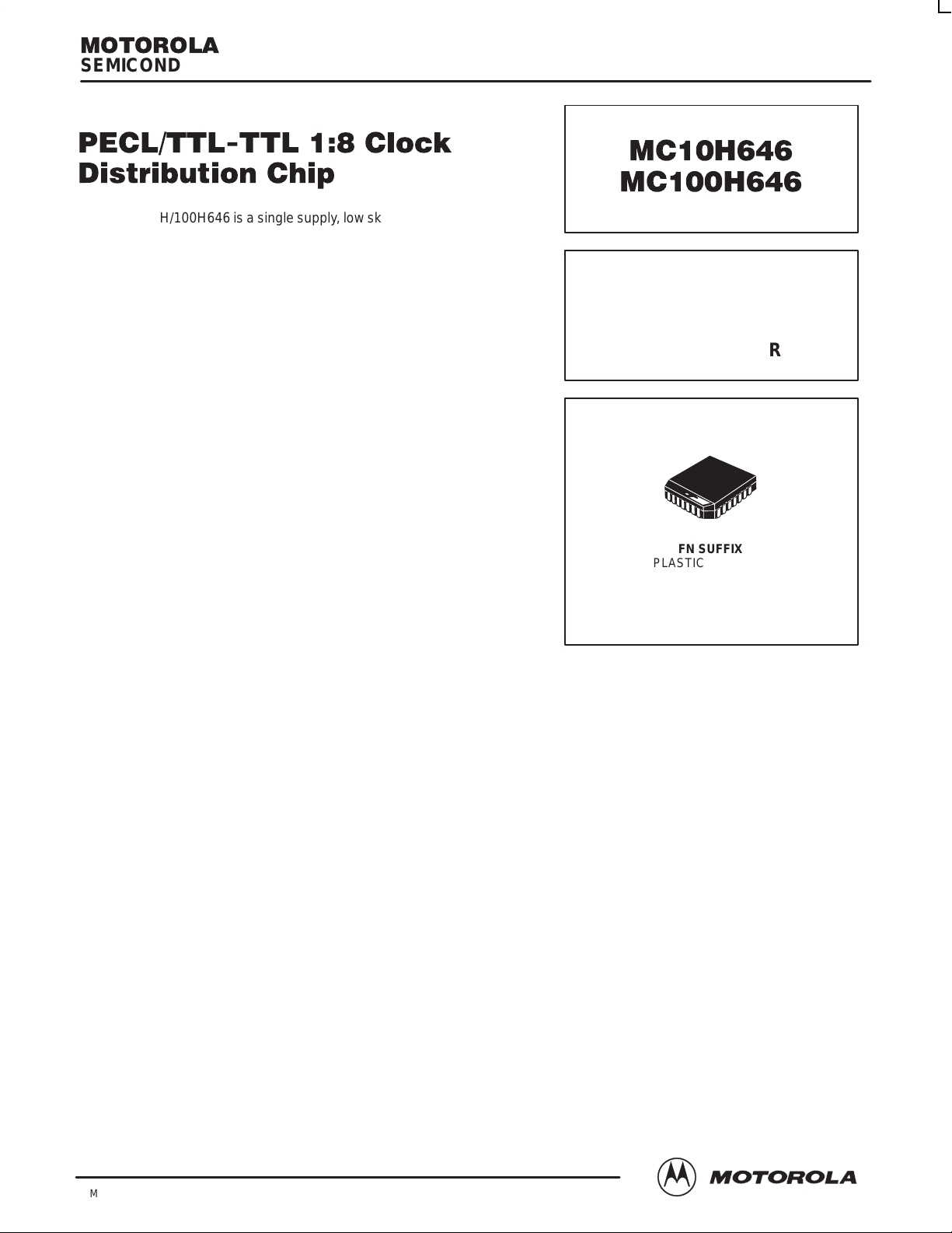
Pinout: 28–Lead PLCC
1
2
3
4
567891011
TCLK
IVT
(Top View)
VEE
IGND
VEE
OGNDQ7
18
17
16
15
14
13
12
VEE
ECLK
EN
IVT
IGND
VCCE
VCCE
VBB
ECLK
PIN NAMES
PIN FUNCTION
OGND
OVT
IGND
IVT
V
EE
V
CCE
ECLK, ECLK
V
BB
Q0–Q7
EN
INTERNAL TTL POWER
TTL Output Ground (0V)
TTL Output VCC (+5.0V)
Internal TTL GND (0V)
Internal TTL VCC (+5.0V)
ECL VEE (0V)
ECL Ground (5.0V)
Differential Signal Input
(PECL)
VBB Reference Output
Signal Outputs (TTL)
Tri–State Enable Input (TTL)
IVT01
OVT01
EN
TCLK
ECLK
ECLK
LOGIC DIAGRAM
Q0
Q1
Q2
Q3
Q4
Q5
Q6
Q7
INTERNAL TTL GROUND IGND01
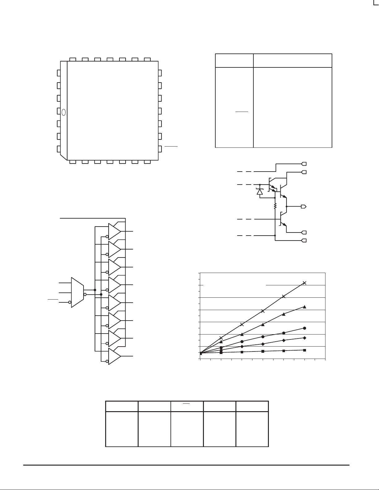
Figure 1. Output Structure
700
P
600
500
400
300
POWER, mW
200
100
Dynamic
P
Total
0
0 20 40 60 80 100 120
Power versus Frequency per Bit
= CL ƒ V
Static
Swing VCC
+ P
Dynamic
FREQUENCY, MHz
= P
Figure 2. Power versus Frequency (Typical)
Q0A
OGND0
300pF
200pF
100pF
50pF
No Load
TRUTH TABLE
TCLK ECLK ECLK EN Q
GND
GND
H
L
X
L = Low Voltage Level; H = High Voltage Level; Z = Tristate
MOTOROLA TIMING SOLUTIONS
L
H
GND
GND
X
H
L
GND
GND
X
2
H
H
H
H
L
L
H
H
L
Z
BR1333 — Rev 6
Page 3

DC CHARACTERISTICS (IVT = OVT = VCCE = 5.0V ±5%)
0°C 25°C 85°C
Symbol Characteristic Min Max Min Max Min Max Unit Condition
V
OH
V
OL
IOS Output Short Circuit Current – – – – – – mA See Note 1
1. The outputs must not be shorted to ground, as this will result in permanent damage to the device. The high drive outputs of this device do not
include a limiting IOS resistor.
Output HIGH Voltage 2.6 –
–
Output LOW Voltage – 0.5 – 0.5 – 0.5 V IOL = 48mA
2.6 –
–
2.6 –
–
V IOH = 24mA
TTL DC CHARACTERISTICS (VT = VE = 5.0 V ±5%)
0°C 25°C 85°C
Symbol Characteristic Min Max Min Max Min Max Unit Condition
V
V
I
I
V
V
V
I
IH
IL
IH
IL
OH
OL
IK
OS
Input HIGH Voltage
Input LOW Voltage
Input HIGH Current 20
Input LOW Current –0.6 –0.6 –0.6 mA VIN = 0.5 V
Output HIGH Voltage 2.5
Output LOW Voltage 0.5 0.5 0.5 V IOL = 24 mA
Input Clamp Voltage –1.2 –1.2 –1.2 V IIN = –18 mA
Output Short Circuit Current –100 –225 –100 –225 –100 –225 mA V
2.0
2.0
0.8
100
2.0
2.5
2.0
0.8
20
100
2.0
2.5
2.0
0.8
20
100
V
µA VIN = 2.7 V
VIN = 7.0 V
V IOH = –3.0 mA
IOH = –24 mA
= 0 V
OUT
10H PECL DC CHARACTERISTICS (IVT = OVT = VCCE = 5.0V ±5%)
0°C 25°C 85°C
Symbol Characteristic Min Typ Max Min Typ Max Min Typ Max Unit Notes
I
IH
I
IL
V
IH
V
IL
V
BB
Input HIGH Current 225 175 175 µA
Input LOW Current 0.5 0.5 0.5 µA
Input HIGH Voltage 3.83 4.16 3.87 4.19 3.94 4.28 V IVT = IVO =
VCCE = 5.0V (1)
Input LOW Voltage 3.05 3.52 3.05 3.52 3.05 3.555 V IVT = IVO =
VCCE = 5.0V (1)
Output Reference Voltage 3.62 3.73 3.65 3.75 3.69 3.81 V IVT = IVO =
VCCE = 5.0V (1)
100H PECL DC CHARACTERISTICS (IVT = OVT = VCCE = 5.0V ±5%)
0°C 25°C 85°C
Symbol Characteristic Min Typ Max Min Typ Max Min Typ Max Unit Notes
I
IH
I
IL
V
IH
V
IL
V
BB
1. ECL VIH, VIL and VBB are referenced to VCCE and will vary 1:1 with the power supply. The levels shown are for IVT = IVO = VCCE = 5.0V
Input HIGH Current 225 175 175 µA
Input LOW Current 0.5 0.5 0.5 µA
Input HIGH Voltage 3.835 4.12 3.835 4.12 3.835 3.835 V IVT = IVO =
VCCE = 5.0V (1)
Input LOW Voltage 3.19 3.525 3.19 3.525 3.19 3.525 V IVT = IVO =
VCCE = 5.0V (1)
Output Reference Voltage 3.62 3.74 3.62 3.74 3.62 3.74 V IVT = IVO =
VCCE = 5.0V (1)
TIMING SOLUTIONS
BR1333 — Rev 6
3 MOTOROLA
Page 4

VCCE pi
DC CHARACTERISTICS (IVT = OVT = VCCE = 5.0V ±5%)
0°C 25°C 85°C
Symbol Characteristic Min Max Min Typ Max Min Max Unit Condition
I
CCL
I
CCH
I
CCZ
AC CHARACTERISTICS (IVT = OVT = VCCE = 5.0V ±5%)
Symbol Characteristic Min Max Min Max Min Max Unit Condition
t
PLH
t
PHL
t
SK(O)
t
SK(PR)
t
SK(P)
tr, t
f
t
PW
t
Stability
F
MAX
1. Output skew defined for identical output transitions.
2. Process skew is valid for VCC = 5.0V ±5%.
3. Parameters guaranteed by t
4. Clock stability is the period variation between two successive rising edges.
5. For series terminated lines. See Applications section for F
6. All AC specifications tested driving 50Ω series terminated transmission lines at 80MHz.
Power Supply Current 185 166 185 185 mA
175 154 175 175 mA
210 210 210
0°C 25°C 85°C
Propagation Delay ECLK to Q
Propagation Delay ECLK to Q
Output Skew Q0, Q3, Q4, Q7
Process Skew ECLK to Q
Pulse Skew ∆t
Rise/Fall Time 0.3 1.5 0.3 1.5 0.3 1.5 ns
Output Pulse Width 66MHz @ 2.0V
Clock Stability ±75 ±75 ±75 ps Note 4, 6
Maximum Input Frequency 80 80 80 MHz Note 5, 6
SK(P)
TCLK to Q
TCLK to Q
Q1, Q2, Q5
Q0–Q7
TCLK to Q
– t
PLH
PHL
66MHz @ 0.8V
60MHz @ 2.0V
60MHz @ 0.8V
and tr, tf specification limits.
4.8
5.1
4.4
4.7
5.5
5.5
6.0
6.0
MAX
5.8
6.4
5.4
6.0
350
350
500
1.0
1.3
1.0 1.0 1.0 ns
enhancement techniques.
5.0
5.3
4.4
4.8
5.5
5.5
6.0
6.0
6.0
6.4
5.4
5.9
350
350
500
1.0
1.1
5.6
5.7
4.8
5.2
5.5
5.5
6.0
6.0
6.6
7.0
5.8
6.5
350
350
500
1.0
1.3
Total all OVT, IVT,
and
ns
ns
ps Note 1, 6
ns Note 2, 6
ns Note 3, 6
p
ns
MOTOROLA TIMING SOLUTIONS
4
BR1333 — Rev 6
Page 5

OUTLINE DIMENSIONS
FN SUFFIX
PLASTIC PLCC PACKAGE
CASE 776–02
ISSUE D
–L–
–N–
28 1
Z
C
G
G1
S
0.010 (0.250) N
L–M
T
S
L–M
T
M
S
S
L–M
T
S
Y BRK
0.007 (0.180) N
B
0.007 (0.180) N
U
M
D
Z
–M–
W
D
V
0.010 (0.250) N
G1X
S
S
L–M
T
S
VIEW D–D
A
0.007 (0.180) N
0.007 (0.180) N
R
E
M
M
S
L–M
T
L–M
T
S
S
S
H
0.007 (0.180) N
M
S
L–M
T
S
K1
0.004 (0.100)
SEATING
J
–T–
PLANE
VIEW S
S
S
K
VIEW S
0.007 (0.180) N
F
M
S
L–M
T
S
NOTES:
1. DATUMS –L–, –M–, AND –N– DETERMINED
WHERE TOP OF LEAD SHOULDER EXITS
PLASTIC BODY AT MOLD PARTING LINE.
2. DIMENSION G1, TRUE POSITION TO BE
MEASURED AT DATUM –T–, SEATING PLANE.
3. DIMENSIONS R AND U DO NOT INCLUDE
MOLD FLASH. ALLOWABLE MOLD FLASH IS
0.010 (0.250) PER SIDE.
4. DIMENSIONING AND TOLERANCING PER
ANSI Y14.5M, 1982.
5. CONTROLLING DIMENSION: INCH.
6. THE PACKAGE TOP MAY BE SMALLER THAN
THE PACKAGE BOTTOM BY UP TO 0.012
(0.300). DIMENSIONS R AND U ARE
DETERMINED AT THE OUTERMOST
EXTREMES OF THE PLASTIC BODY
EXCLUSIVE OF MOLD FLASH, TIE BAR
BURRS, GATE BURRS AND INTERLEAD
FLASH, BUT INCLUDING ANY MISMATCH
BETWEEN THE TOP AND BOTTOM OF THE
PLASTIC BODY.
7. DIMENSION H DOES NOT INCLUDE DAMBAR
PROTRUSION OR INTRUSION. THE DAMBAR
PROTRUSION(S) SHALL NOT CAUSE THE H
DIMENSION TO BE GREATER THAN 0.037
(0.940). THE DAMBAR INTRUSION(S) SHALL
NOT CAUSE THE H DIMENSION TO BE
SMALLER THAN 0.025 (0.635).
DIM MIN MAX MIN MAX
A 0.485 0.495 12.32 12.57
B 0.485 0.495 12.32 12.57
C 0.165 0.180 4.20 4.57
E 0.090 0.110 2.29 2.79
F 0.013 0.019 0.33 0.48
G 0.050 BSC 1.27 BSC
H 0.026 0.032 0.66 0.81
J 0.020 ––– 0.51 –––
K 0.025 ––– 0.64 –––
R 0.450 0.456 11.43 11.58
U 0.450 0.456 11.43 11.58
V 0.042 0.048 1.07 1.21
W 0.042 0.048 1.07 1.21
X 0.042 0.056 1.07 1.42
Y ––– 0.020 ––– 0.50
Z 2 10 2 10
____
G1 0.410 0.430 10.42 10.92
K1 0.040 ––– 1.02 –––
MILLIMETERSINCHES
TIMING SOLUTIONS
BR1333 — Rev 6
5 MOTOROLA
Page 6

Motorola reserves the right to make changes without further notice to any products herein. Motorola makes no warranty , representation or guarantee regarding
the suitability of its products for any particular purpose, nor does Motorola assume any liability arising out of the application or use of any product or circuit, and
specifically disclaims any and all liability, including without limitation consequential or incidental damages. “T ypical” parameters which may be provided in Motorola
data sheets and/or specifications can and do vary in different applications and actual performance may vary over time. All operating parameters, including “Typicals”
must be validated for each customer application by customer’s technical experts. Motorola does not convey any license under its patent rights nor the rights of
others. Motorola products are not designed, intended, or authorized for use as components in systems intended for surgical implant into the body, or other
applications intended to support or sustain life, or for any other application in which the failure of the Motorola product could create a situation where personal injury
or death may occur. Should Buyer purchase or use Motorola products for any such unintended or unauthorized application, Buyer shall indemnify and hold Motorola
and its officers, employees, subsidiaries, affiliates, and distributors harmless against all claims, costs, damages, and expenses, and reasonable attorney fees
arising out of, directly or indirectly, any claim of personal injury or death associated with such unintended or unauthorized use, even if such claim alleges that
Motorola was negligent regarding the design or manufacture of the part. Motorola and are registered trademarks of Motorola, Inc. Motorola, Inc. is an Equal
Opportunity/Affirmative Action Employer.
How to reach us:
USA/EUROPE /Locations Not Listed: Motorola Literature Distribution; JAPAN: Nippon Motorola Ltd.; Tatsumi–SPD–JLDC, 6F Seibu–Butsuryu–Center,
P.O. Box 5405; Denver, Colorado 80217. 303–675–2140 or 1–800–441–2447 3–14–2 Tatsumi Koto–Ku, Tokyo 135, Japan. 81–3–3521–8315
Mfax: RMFAX0@email.sps.mot.com – TOUCHT ONE 602–244–6609 ASIA/PACIFIC: Motorola Semiconductors H.K. Ltd.; 8B Tai Ping Industrial Park,
INTERNET: http://www.mot.com/sps/ 51 Ting Kok Road, Tai Po, N.T., Hong Kong. 852–26629298
MOTOROLA TIMING SOLUTIONS
◊
6
*MC10H646/D*
MC10H646/D
BR1333 — Rev 6
 Loading...