

Page 1
MOTOROLA
SEMICONDUCTOR TECHNICAL DATA
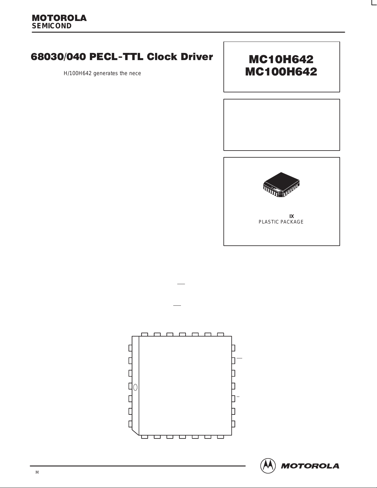
68030/040 PECL-TTL Clock Driver
The MC10H/100H642 generates the necessary clocks for the 68030,
68040 and similar microprocessors. It is guaranteed to meet the clock
specifications required by the 68030 and 68040 in terms of part–to–part
skew, within–part skew and also duty cycle skew.
The user has a choice of using either TTL or PECL (ECL referenced to
+5.0V) for the input clock. TTL clocks are typically used in present MPU
systems. However, as clock speeds increase to 50MHz and beyond, the
inherent superiority of ECL (particularly differential ECL) as a means of
clock signal distribution becomes increasingly evident. The H642 also
uses differential PECL internally to achieve its superior skew
characteristic.
The H642 includes divide–by–two and divide–by–four stages, both to
achieve the necessary duty cycle skew and to generate MPU clocks as
required. A typical 50MHz processor application would use an input clock
running at 100MHz, thus obtaining output clocks at 50MHz and 25MHz
(see Logic Diagram).
The 10H version is compatible with MECL 10H ECL logic levels,
while the 100H version is compatible with 100K levels (referenced to
+5.0V).
• Generates Clocks for 68030/040
• Meets 030/040 Skew Requirements
• TTL or PECL Input Clock
• Extra TTL and PECL Power/Ground Pins
• Asynchronous Reset
• Single +5.0V Supply
MC10H642
MC100H642
68030/040
PECL–TTL CLOCK
DRIVER
26
45
FN SUFFIX
PLASTIC PACKAGE
CASE 776–02
11
Function
Reset(R):
Select(SEL):
LOW on RESET forces all Q outputs LOW.
LOW selects the ECL input source (DE/DE).
HIGH selects the TTL input source (DT).
The H642 also contains circuitry to force a stable input state of the ECL differential input pair , should both sides be left open. In
this Case, the DE side of the input is pulled LOW, and DE
Power Up:
The device is designed to have positive edges of the ÷2 and ÷4 outputs synchronized at Power Up.
VT VT Q1 GT GT Q0 VT
25 24 23 22 21 20 19
Q2
26
GT
27
GT
28
Pinout: 28–Lead PLCC
567891011
Q5
GT GT Q6 Q7 VT SEL
VT
VT
Q3
1
2
3
4
goes HIGH.
(Top View)
18
V
BB
17
DE
16
DE
VE
15
R
14
GE
13
12
DTQ4
9/96
Motorola, Inc. 1996
2–1
REV 4
Page 2
MC10H642 MC100H642
LOGIC DIAGRAM
TTL Outputs
Q7
TTL/ECL Clock Inputs
V
BB
DE
DE
DT
SEL
TTL Control Inputs
R
MUX
÷4
÷2
Q6
Q5
Q4
Q3
Q2
Q1
Q0
PIN NAMES
Pin Symbol Description Pin Symbol Description
81
82
83
84
85
86
87
88
89
10
11
12
13
14
**Divide by 2
**Divide by 4
Q3
VT
VT
Q4
Q5
GT
GT
Q6
Q7
VT
SEL
DT
GE
R
Signal Output (TTL)**
TTL VCC (+5.0V)
TTL VCC (+5.0V)
Signal Output (TTL)**
Signal Output (TTL)**
TTL Ground (0V)
TTL Ground (0V)
Signal Output (TTL)**
Signal Output (TTL)**
TTL VCC (+5.0V)
Input Select (TTL)
TTL Signal Input
ECL Ground (0V)
Reset (TTL)
15
16
17
18
19
20
21
22
23
24
25
26
27
28
V
VE
DE
DE
BB
VT
Q0
GT
GT
Q1
VT
VT
Q2
GT
GT
ECL VCC (+5.0V)
ECL Signal Input (Non–Inverting)
ECL Signal Input (Inverting)
VBB Reference Output
TTL VCC (+5.0V)
Signal Output (TTL)*
TTL Ground (0V)
TTL Ground (0V)
Signal Output (TTL)*
TTL VCC (+5.0V)
TTL VCC (+5.0V)
Signal Output (TTL)**
TTL Ground (0V)
TTL Ground (0V)
MOTOROLA MECL Data
2–2
DL122 — Rev 6
Page 3
MC10H642 MC100H642
AC CHARACTERISTICS (VT = VE = 5.0V ±5%)
TA = 0°C TA = 25°C TA = 85°C
Symbol Characteristic Min Max Min Max Min Max Unit Condition
t
PLH
tskpp Part–to–Part Skew 1.0 1.0 1.0 ns
tskwd* Within–Device Skew 0.5 0.5 0.5 ns
t
PLH
tskpp Part–to–Part Skew All
tskwd Within–Device Skew 1.0 1.0 1.0 ns CL = 25pF
t
PD
t
R
t
F
f
MAX
RPW Reset Pulse Width 1.5 1.5 1.5 ns
RRT Reset Recovery Time 1.25 1.25 1.25 ns
* Within–Device Skew defined as identical transactions on similar paths through a device.
** NOTE: MAX Frequency is 135MHz.
Propagation Delay
D to Output
Propagation Delay
D to Output
Propagation Delay
R to Output
Output Rise/Fall Time
0.8 V to 2.0 V
** Maximum Input Frequency 100 100 100 MHz CL = 25pF
Q2–Q7
C ECL
C TTL
Q0, Q1
C ECL
C TTL
Outputs
All
Outputs
All
Outputs
4.70
4.70
4.30
4.30
4.3 6.3 4.0 6.0 4.5 6.5 ns CL = 25pF
5.70
5.70
5.30
5.30
2.0 2.0 2.0 ns CL = 25pF
2.5
2.5
4.75
4.75
4.50
4.50
5.75
5.75
5.50
5.50
2.5
2.5
4.60
4.50
4.25
4.25
5.60
5.50
5.25
5.25
2.5
2.5
ns CL = 25pF
ns CL = 25pF
ns CL = 25pF
10H PECL CHARACTERISTICS (VT = VE = 5.0V ±5%)
TA = 0°C TA = 25°C TA = 85°C
Symbol Characteristic Min Max Min Max Min Max Unit Condition
I
IH
I
IL
V
IH
V
IL
V
BB
Input HIGH Current
Input LOW Current
* NOTE
Input HIGH Voltage
Input LOW Voltage
* NOTE
Output Reference Voltage 3.62 3.73 3.65 3.75 3.69 3.81 V
0.5
3.83
3.05
225
4.16
3.52
0.5
3.87
3.05
175
4.19
3.52
0.5
3.94
3.05
175 µA
4.28
3.555
V VEE = 5.0V
100H PECL CHARACTERISTICS (VT = VE = 5.0V ±5%)
TA = 0°C TA = 25°C TA = 85°C
Symbol Characteristic Min Max Min Max Min Max Unit Condition
I
IH
I
IL
V
IH
V
IL
V
BB
*NOTE: PECL LEVELS are referenced to VCC and will vary 1:1 with the power supply. The VALUES shown are for VCC = 5.0V.
Input HIGH Current
Input LOW Current
* NOTE
Input HIGH Voltage
Input LOW Voltage
* NOTE
Output Reference Voltage 3.620 3.740 3.620 3.740 3.620 3.740 V
0.5
3.835
3.190
225
4.120
3.525
0.5
3.835
3.190
175
4.120
3.525
0.5
3.835
3.190
175 µA
4.120
3.525
V VEE = 5.0V
DL122 — Rev 6
2–3 MOTOROLAMECL Data
Page 4

MC10H642 MC100H642
10H/100H DC CHARACTERISTICS (VT = VE = 5.0V ±5%)
TA = 0°C TA = 25°C TA = 85°C
Symbol Characteristic Min Max Min Max Min Max Unit Condition
I
EE
I
CCH
I
CCL
10H/100H TTL DC CHARACTERISTICS (VT = VE = 5.0V ±5%)
Symbol Characteristic Min Max Min Max Min Max Unit Condition
V
IH
V
IL
I
IH
I
IL
V
OH
V
OL
V
IK
I
OS
Power Supply Current PECL 57 57 57 mA VE Pin
TTL 30 30 30 mA Total All VT Pins
30 30 30 mA
TA = 0°C TA = 25°C TA = 85°C
Input HIGH Voltage
Input LOW Voltage
Input HIGH Current 20
Input LOW Current –0.6 –0.6 –0.6 mA VIN = 0.5V
Output HIGH Voltage 2.5
Output LOW Voltage 0.5 0.5 0.5 V IOL = 24mA
Input Clamp Voltage –1.2 –1.2 –1.2 V IIN = –18mA
Output Short Circuit Current –100 –225 –100 –225 –100 –225 mA V
2.0
2.0
0.8
100
2.0
2.5
2.0
0.8
20
100
2.0
2.5
2.0
0.8
20
100
V
µA VIN = 2.7V
VIN = 7.0V
V IOH = –3.0mA
IOH = –15mA
= 0V
OUT
10/100H642
DUTY CYCLE CONTROL
T o maintain a duty cycle of ±5% at 50 MHz, limit the load capacitance and/or power supply variation as shown in Figures 1 and 2.
For a ±2.5% duty cycle limit, see Figures 3 and 4. Figures 5 and 6 show duty cycle variation with temperature. Figure 7 shows typical
TPD versus load. Figure 8 shows reset recovery time. Figure 9 shows output states after power up.
Best duty cycle control is obtained with a single µP load and minimum line length.
MOTOROLA MECL Data
2–4
DL122 — Rev 6
Page 5

MC10H642 MC100H642
11
11
10
POSITIVE PULSE WIDTH (ns)
9
0 102030405060
CAPACITIVE LOAD (pF)
Figure 1. MC10H642 Positive PW versus Load
@ ±5% VCC, TA = 25°C
10.6
10.4
10.2
10.0
9.8
9.6
POSITIVE PULSE WIDTH (ns)
9.4
4.75
5.00
5.25
4.875
5.00
5.125
10
NEGATIVE PULSE WIDTH (ns)
9
0102030405060
CAPACITIVE LOAD (pF)
Figure 2. MC10H642 Negative PW versus
Load
@ ±5% VCC, TA = 25°C
10.8
10.6
10.4
10.2
10.0
9.8
NEGATIVE PULSE WIDTH (ns)
9.6
4.75
5.00
5.25
4.875
5.00
5.125
9.2
0 102030405060
CAPACITIVE LOAD (pF)
Figure 3. MC10H642 Positive PW versus Load
@ ±2.5% VCC, TA = 25°C
10.4
10.2
10.0
9.8
9.6
POSITIVE PULSE WIDTH (ns)
9.4
020406080100
TEMPERATURE (°C)
0 pF
25 pF
50 pF
Figure 5. MC10H642 Positive PW versus T emperature,
VCC = 5.0V
9.4
0 102030405060
CAPACITIVE LOAD (pF)
Figure 4. MC10H642 Negative PW versus Load
@ ±2.5% VCC, TA = 25°C
10.5
10.3
10.1
9.9
9.7
NEGATIVE PULSE WIDTH (ns)
9.5
0 20 40 60 80 100
TEMPERATURE (°C)
Figure 6. MC10H642 Negative PW versus
T emperature, VCC = 5.0V
0 pF
25 pF
50 pF
DL122 — Rev 6
2–5 MOTOROLAMECL Data
Page 6

MC10H642 MC100H642
6.2
6.0
DT
RESET, R
Q0 Q1
5.8
Tpd (ns)
5.6
5.4
5.2
0 102030405060
CAPACITIVE (pF)
4.75
5.00
5.25
Figure 7. MC10H642 + Tpd versus Load, VCC ±5%, TA = 25°C
(Overshoot at 50 MHz with no load makes graph non linear)
R
t
R
t
pw
rec
Q2 Q7
D
in
Q0.Q1
Q4 & Q5
Q2 Q7
MC10/100H642
Figure 8. Clock Phase and Reset Recovery Time After Reset Pulse
MC10/100H642
After Power Up
Figure 9. Outputs
Q2 Q7 will Synchronize with Pos Edges of Din & Q0 Q1
MOTOROLA MECL Data
2–6
DL122 — Rev 6
Page 7

SWITCHING CIRCUIT AND WAVEFORMS
MC10H642 MC100H642
Switching Circuit PECL:
PECL
USE 0.1 µF CAPACITORS
FOR DECOUPLING.
PULSE
GENERATOR
USE OSCILLOSCOPE
INTERNAL 50 Ω LOAD
FOR TERMINATION.
50 Ω COAX
CH A
WAVEFORMS: Rise and Fall Times
PECL/TTL
V
EE
IN OUT
Ω
COAX50
OSCILLOSCOPE
DEVICE
UNDER
TEST
VCC & V
CCO
CH B
TTL
450 Ω
Ω
COAX50
DEVICE
UNDER
TEST
t
OC
PZL
, t
PLZ
50 pF
Propagation Delay — Single Ended
PECL/TTL
+7 V OPEN
500 Ω
ALL
OTHERS
R1
500 Ω
R2
50%/1.5 V
V
80%/2.0 V
V
out
T
rise
T
fall
20%/0.8 V
in
T
pd++
50%/1.5 V
V
out
T
pd––
DL122 — Rev 6
2–7 MOTOROLAMECL Data
Page 8

MC10H642 MC100H642
OUTLINE DIMENSIONS
FN SUFFIX
PLASTIC PLCC PACKAGE
CASE 776–02
ISSUE D
–L–
–N–
28 1
Z
C
G
G1
S
0.010 (0.250) N
L–M
T
S
L–M
T
M
S
S
L–M
T
S
Y BRK
0.007 (0.180) N
B
0.007 (0.180) N
U
M
D
Z
–M–
W
D
V
0.010 (0.250) N
G1X
S
S
L–M
T
S
VIEW D–D
A
0.007 (0.180) N
0.007 (0.180) N
R
E
M
M
S
L–M
T
L–M
T
S
S
S
H
0.007 (0.180) N
M
S
L–M
T
S
K1
0.004 (0.100)
SEATING
J
–T–
PLANE
VIEW S
S
S
K
VIEW S
0.007 (0.180) N
F
M
S
L–M
T
S
NOTES:
1. DATUMS –L–, –M–, AND –N– DETERMINED
WHERE TOP OF LEAD SHOULDER EXITS
PLASTIC BODY AT MOLD PARTING LINE.
2. DIMENSION G1, TRUE POSITION TO BE
MEASURED AT DATUM –T–, SEATING PLANE.
3. DIMENSIONS R AND U DO NOT INCLUDE
MOLD FLASH. ALLOWABLE MOLD FLASH IS
0.010 (0.250) PER SIDE.
4. DIMENSIONING AND TOLERANCING PER
ANSI Y14.5M, 1982.
5. CONTROLLING DIMENSION: INCH.
6. THE PACKAGE TOP MAY BE SMALLER THAN
THE PACKAGE BOTTOM BY UP TO 0.012
(0.300). DIMENSIONS R AND U ARE
DETERMINED AT THE OUTERMOST
EXTREMES OF THE PLASTIC BODY
EXCLUSIVE OF MOLD FLASH, TIE BAR
BURRS, GATE BURRS AND INTERLEAD
FLASH, BUT INCLUDING ANY MISMATCH
BETWEEN THE TOP AND BOTTOM OF THE
PLASTIC BODY.
7. DIMENSION H DOES NOT INCLUDE DAMBAR
PROTRUSION OR INTRUSION. THE DAMBAR
PROTRUSION(S) SHALL NOT CAUSE THE H
DIMENSION TO BE GREATER THAN 0.037
(0.940). THE DAMBAR INTRUSION(S) SHALL
NOT CAUSE THE H DIMENSION TO BE
SMALLER THAN 0.025 (0.635).
DIM MIN MAX MIN MAX
A 0.485 0.495 12.32 12.57
B 0.485 0.495 12.32 12.57
C 0.165 0.180 4.20 4.57
E 0.090 0.110 2.29 2.79
F 0.013 0.019 0.33 0.48
G 0.050 BSC 1.27 BSC
H 0.026 0.032 0.66 0.81
J 0.020 ––– 0.51 –––
K 0.025 ––– 0.64 –––
R 0.450 0.456 11.43 11.58
U 0.450 0.456 11.43 11.58
V 0.042 0.048 1.07 1.21
W 0.042 0.048 1.07 1.21
X 0.042 0.056 1.07 1.42
Y ––– 0.020 ––– 0.50
Z 2 10 2 10
____
G1 0.410 0.430 10.42 10.92
K1 0.040 ––– 1.02 –––
MILLIMETERSINCHES
MOTOROLA MECL Data
2–8
DL122 — Rev 6
Page 9

MC10H642 MC100H642
Motorola reserves the right to make changes without further notice to any products herein. Motorola makes no warranty , representation or guarantee regarding
the suitability of its products for any particular purpose, nor does Motorola assume any liability arising out of the application or use of any product or circuit, and
specifically disclaims any and all liability, including without limitation consequential or incidental damages. “T ypical” parameters which may be provided in Motorola
data sheets and/or specifications can and do vary in different applications and actual performance may vary over time. All operating parameters, including “Typicals”
must be validated for each customer application by customer’s technical experts. Motorola does not convey any license under its patent rights nor the rights of
others. Motorola products are not designed, intended, or authorized for use as components in systems intended for surgical implant into the body, or other
applications intended to support or sustain life, or for any other application in which the failure of the Motorola product could create a situation where personal injury
or death may occur. Should Buyer purchase or use Motorola products for any such unintended or unauthorized application, Buyer shall indemnify and hold Motorola
and its officers, employees, subsidiaries, affiliates, and distributors harmless against all claims, costs, damages, and expenses, and reasonable attorney fees
arising out of, directly or indirectly, any claim of personal injury or death associated with such unintended or unauthorized use, even if such claim alleges that
Motorola was negligent regarding the design or manufacture of the part. Motorola and are registered trademarks of Motorola, Inc. Motorola, Inc. is an Equal
Opportunity/Affirmative Action Employer.
How to reach us:
USA/EUROPE/ Locations Not Listed: Motorola Literature Distribution; JAPAN: Nippon Motorola Ltd.; Tatsumi–SPD–JLDC, 6F Seibu–Butsuryu–Center,
P.O. Box 20912; Phoenix, Arizona 85036. 1–800–441–2447 or 602–303–5454 3–14–2 Tatsumi Koto–Ku, Tokyo 135, Japan. 03–81–3521–8315
MFAX: RMF AX0@email.sps.mot.com – T OUCHTONE 602–244–6609 ASIA/ PACIFIC: Motorola Semiconductors H.K. Ltd.; 8B Tai Ping Industrial Park,
INTERNET: http://Design–NET .com 51 Ting Kok Road, Tai Po, N.T., Hong Kong. 852–26629298
MC10H642/D
DL122 — Rev 6
◊
2–9 MOTOROLAMECL Data
*MC10H642/D*
 Loading...