

Page 1
SEMICONDUCTOR TECHNICAL DATA
2–311
REV 1
Motorola, Inc. 1996
9/96
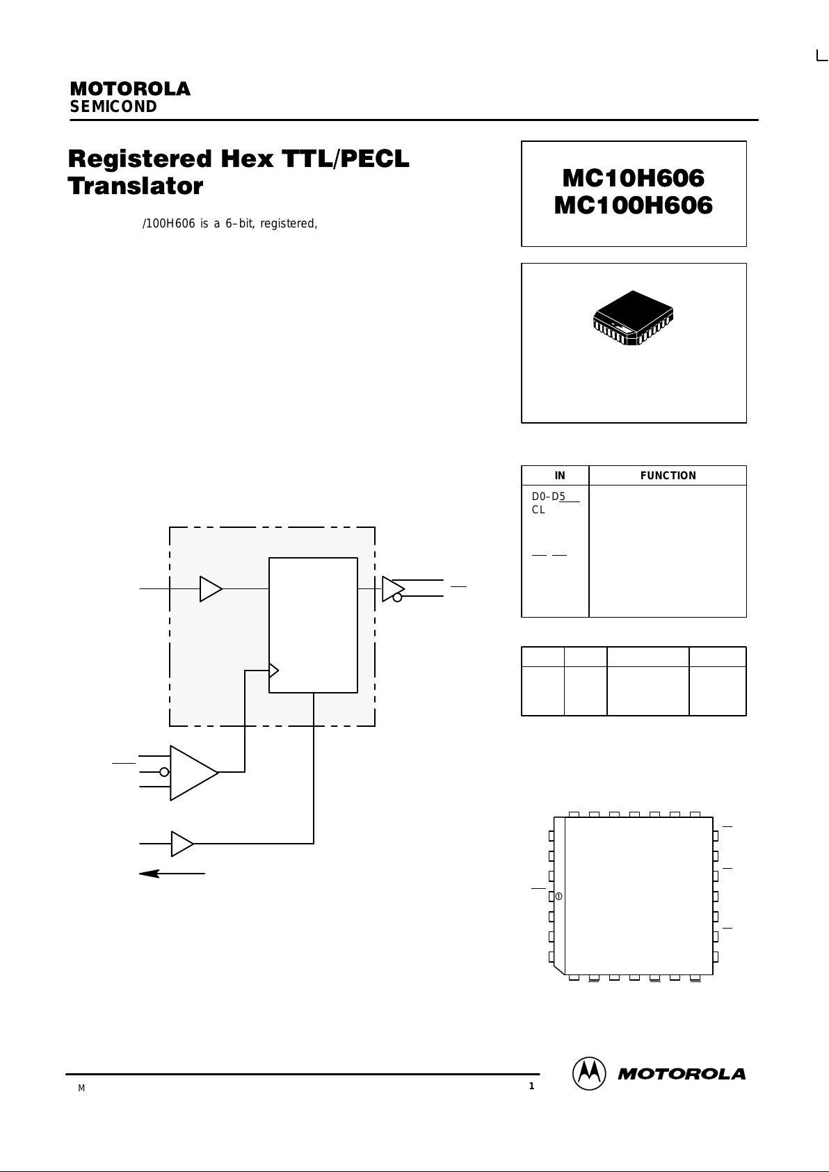
The MC10/100H606 is a 6–bit, registered, single supply TTL to PECL
translator. The device features dif ferential PECL outputs as well as a choice
between either a differential PECL clock input or a TTL clock input. The
asynchronous master reset control is a PECL level input.
With its differential PECL outputs and TTL inputs the H606 device is
ideally suited for the transmit function of a HPPI bus type board–to–board
interface application. The on chip registers simplify the task of synchronizing
the data between the two boards.
The device is available in either ECL standard: the MECL 10H device is
compatible with MECL 10KH logic levels, with a VCC of +5 volts; while the
100H device is compatible with 100K logic levels, with a VCC of +5 volts.
• Differential 50Ω ECL Outputs
• Choice Between Differential PECL or TTL Clock Input
• Single Power Supply
• Multiple Power and Ground Pins to Minimize Noise
*
D
n
Q
n
Q
n
MR
TCLK
CLK
CLK
V
BB
1 OF 6 BITS
D
CLK
R
Q
LOGIC SYMBOL
*
1. When using PECL inputs, TCLK must be tied to ground (0V).
2. When using only one PECL input, the unused PECL input must be tied
to VBB, and TCLK must be tied to ground (0V).
3. When using TCLK, both PECL inputs must be tied to ground (0V).
MECL 10H is a trademark of Motorola, Inc.
Pinout: 28–Lead PLCC (Top View)
PIN NAMES
PIN FUNCTION
D0–D5
CLK, CLK
TCLK
MR
Q0–Q5
Q0
–Q5
V
CCE
V
CCT
GND
TTL Data Inputs
Differential PECL Clock Input
TTL Clock Input
PECL Master Reset Input
True PECL Outputs
Inverted PECL Outputs
PECL VCC (+5.0V)
TTL VCC (+5.0V)
TTL/PECL Ground
D0
567891011
25 24 23 22 21 20 19
TCLK
V
BB
CLK
CLK
MR
V
CCE
Q4
Q5
Q5
Q4
V
CCE
Q3
Q3
26
27
28
2
3
4
18
17
16
14
13
12
15
D1 D2 V
CCT
D3 D4 D5 V
CCE
Q0 Q0
GND Q1 Q1 Q2 Q2
FN SUFFIX
PLASTIC PACKAGE
CASE 776–02
Dn
L
H
X
TRUTH TABLE
MR
L
L
H
TCLK/CLK
Z
Z
X
Qn+1
L
H
L
Z = LOW to HIGH Transition
Page 2
MC10H606 MC100H606
MOTOROLA MECL Data
DL122 — Rev 6
2–312
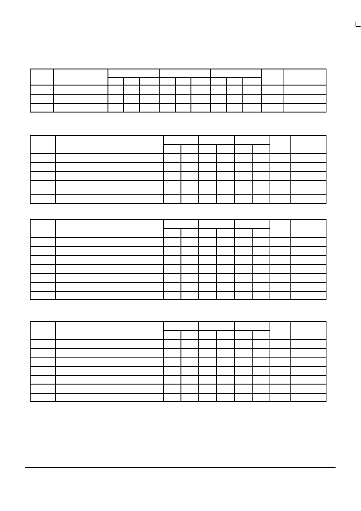
DC CHARACTERISTICS (V
CCT
= V
CCE
= 5.0V ±5%)
TA = 0°C TA = + 25°C TA = + 85°C
Symbol Characteristic Min Typ Max Min Typ Max Min Typ Max Unit Condition
I
CCTL
Supply Current 18 30 18 30 18 30 mA Outputs LOW
I
CCTH
Supply Current 13 25 13 25 13 25 mA Outputs HIGH
I
GND
Supply Current 75 90 75 90 75 95 mA
TTL DC CHARACTERISTICS (V
CCT
= V
CCE
= 5.0V ±5%)
TA = 0°C TA = 25°C TA = 85°C
Symbol Characteristic Min Max Min Max Min Max Unit Condition
V
IH
Input HIGH Voltage 2.0 2.0 2.0 V
V
IL
Input LOW Voltage 0.8 0.8 0.8 V
V
IK
Input Clamp Voltage –1.2 –1.2 –1.2 V IIN = –18mA
I
IH
Input HIGH Current 20
100
20
100
20
100
V VIN = 2.7V
VIN = 7.0V
I
IL
Input LOW Current –0.6 –0.6 –0.6 mA VIN = 0.5V
10H PECL DC CHARACTERISTICS (V
CCT
= V
CCE
= 5.0V ±5%)
TA = 0°C TA = 25°C TA = 85°C
Symbol Characteristic Min Max Min Max Min Max Unit Condition
I
INH
Input HIGH Current 255 145 145 µ
A
I
INL
Input LOW Current 0.5 0.5 0.5 µ
A
V
IH
Input HIGH Voltage (Note 1.) 3830 4160 3870 4190 3930 4280 mV V
CCT
= 5.0V
V
IL
Input LOW Voltage (Note 1.) 3050 3520 3050 3520 3050 3555 mV V
CCT
= 5.0V
V
OH
Output HIGH Voltage (Note 1.) 3980 4160 4020 4190 4080 4270 mV V
CCT
= 5.0V
V
OL
Output LOW Voltage (Note 1.) 3050 3370 3050 3370 3050 3400 mV V
CCT
= 5.0V
V
BB
Output Bias Voltage (Note 1.) 3600 3710 3630 3730 3670 3790 mV V
CCT
= 5.0V
1. PECL VIL, VIH, VOL, VOH VBB are given for V
CCT
= V
CCE
= 5.0V and will vary 1:1 with the power supply.
100H PECL DC CHARACTERISTICS (V
CCT
= V
CCE
= 5.0V ±5%)
TA = 0°C TA = 25°C TA = 85°C
Symbol Characteristic Min Max Min Max Min Max Unit Condition
I
INH
Input HIGH Current 255 145 145 µ
A
I
INL
Input LOW Current 0.5 0.5 0.5 µ
A
V
IH
Input HIGH Voltage (Note 1.) 3835 4120 3835 4120 3835 4120 mV V
CCT
= 5.0V
V
IL
Input LOW Voltage (Note 1.) 3190 3525 3190 3525 3190 3525 mV V
CCT
= 5.0V
V
OH
Output HIGH Voltage (Note 1.) 3975 4120 3975 4120 3975 4120 mV V
CCT
= 5.0V
V
OL
Output LOW Voltage (Note 1.) 3190 3380 3190 3380 3190 3380 mV V
CCT
= 5.0V
V
BB
Output Bias Voltage (Note 1.) 3600 3720 3600 3720 3600 3720 mV V
CCT
= 5.0V
1. PECL VIL, VIH, VOL, VOH VBB are given for V
CCT
= V
CCE
= 5.0V and will vary 1:1 with the power supply.
Page 3

MC10H606 MC100H606
2–313 MOTOROLAMECL Data
DL122 — Rev 6
AC CHARACTERISTICS (V
CCT
= V
CCE
= 5.0V ±5%)
TA = 0°C TA = + 25°C TA = + 85°C
Symbol Characteristic Min Typ Max Min Typ Max Min Typ Max Unit Condition
t
PD
Propagation Delay
TCLK++
1.75 3.75 1.75 3.00 3.75 1.75 3.75 ns CL = 50pF
t
PD
Propagation Delay
TCLK+–
1.75 3.75 1.75 3.00 3.75 1.75 3.75 ns CL = 50pF
t
PD
Propagation Delay
CLK++
1.50 3.50 1.50 2.50 3.50 1.50 3.50 ns CL = 50pF
t
PD
Propagation Delay
CLK+–
1.50 3.50 1.50 2.50 3.50 1.50 3.50 ns CL = 50pF
t
PD
Propagation Delay
MR+–
1.50 3.50 1.50 2.50 3.50 1.75 3.75 ns CL = 50pF
t
SKEW
Device Skew
Part–to–Part
Within Device
2.0
0.5
1.0
0.3
2.0
0.5
2.0
0.5
ns CL = 50pF
t
S
Setup Time 1.5 0.5 1.5 0.5 1.5 0.5 ns CL = 50pF
t
H
Hold Time 1.5 0.5 1.5 0.5 1.5 0.5 ns CL = 50pF
t
PW
Minimum Pulse Width
CLK
1.5 1.5 1.0 1.5 ns CL = 50pF
t
PW
Minimum Pulse WidthMR1.5 1.5 1.5 ns CL = 50pF
t
r
Rise Time 2.0 1.0 2.0 2.0 ns CL = 50pF
t
f
Fall Time 2.0 1.0 2.0 2.0 ns CL = 50pF
t
RES/REC
Reset/Recovery Time 2.5 2.0 2.5 2.0 2.5 2.0 ns CL = 50pF
Page 4

MC10H606 MC100H606
MOTOROLA MECL Data
DL122 — Rev 6
2–314
OUTLINE DIMENSIONS
FN SUFFIX
PLASTIC PLCC PACKAGE
CASE 776–02
ISSUE D
NOTES:
1. DATUMS –L–, –M–, AND –N– DETERMINED
WHERE TOP OF LEAD SHOULDER EXITS
PLASTIC BODY AT MOLD PARTING LINE.
2. DIMENSION G1, TRUE POSITION TO BE
MEASURED AT DATUM –T–, SEATING PLANE.
3. DIMENSIONS R AND U DO NOT INCLUDE
MOLD FLASH. ALLOWABLE MOLD FLASH IS
0.010 (0.250) PER SIDE.
4. DIMENSIONING AND TOLERANCING PER
ANSI Y14.5M, 1982.
5. CONTROLLING DIMENSION: INCH.
6. THE PACKAGE TOP MAY BE SMALLER THAN
THE PACKAGE BOTTOM BY UP TO 0.012
(0.300). DIMENSIONS R AND U ARE
DETERMINED AT THE OUTERMOST
EXTREMES OF THE PLASTIC BODY
EXCLUSIVE OF MOLD FLASH, TIE BAR
BURRS, GATE BURRS AND INTERLEAD
FLASH, BUT INCLUDING ANY MISMATCH
BETWEEN THE TOP AND BOTTOM OF THE
PLASTIC BODY.
7. DIMENSION H DOES NOT INCLUDE DAMBAR
PROTRUSION OR INTRUSION. THE DAMBAR
PROTRUSION(S) SHALL NOT CAUSE THE H
DIMENSION TO BE GREATER THAN 0.037
(0.940). THE DAMBAR INTRUSION(S) SHALL
NOT CAUSE THE H DIMENSION TO BE
SMALLER THAN 0.025 (0.635).
–N–
–M–
–L–
V
W
D
D
Y BRK
28 1
VIEW S
S
L–M
S
0.010 (0.250) N
S
T
S
L–M
M
0.007 (0.180) N
S
T
0.004 (0.100)
G1
G
J
C
Z
R
E
A
SEATING
PLANE
S
L–M
M
0.007 (0.180) N
S
T
–T–
B
S
L–M
S
0.010 (0.250) N
S
T
S
L–M
M
0.007 (0.180) N
S
T
U
S
L–M
M
0.007 (0.180) N
S
T
Z
G1X
VIEW D–D
S
L–M
M
0.007 (0.180) N
S
T
K1
VIEW S
H
K
F
S
L–M
M
0.007 (0.180) N
S
T
DIM MIN MAX MIN MAX
MILLIMETERSINCHES
A 0.485 0.495 12.32 12.57
B 0.485 0.495 12.32 12.57
C 0.165 0.180 4.20 4.57
E 0.090 0.1 10 2.29 2.79
F 0.013 0.019 0.33 0.48
G 0.050 BSC 1.27 BSC
H 0.026 0.032 0.66 0.81
J 0.020 ––– 0.51 –––
K 0.025 ––– 0.64 –––
R 0.450 0.456 11.43 11.58
U 0.450 0.456 11.43 11.58
V 0.042 0.048 1.07 1.21
W 0.042 0.048 1.07 1.21
X 0.042 0.056 1.07 1.42
Y ––– 0.020 ––– 0.50
Z 2 10 2 10
G1 0.410 0.430 10.42 10.92
K1 0.040 ––– 1.02 –––
____
Page 5

MC10H606 MC100H606
2–315 MOTOROLAMECL Data
DL122 — Rev 6
Motorola reserves the right to make changes without further notice to any products herein. Motorola makes no warranty , representation or guarantee regarding
the suitability of its products for any particular purpose, nor does Motorola assume any liability arising out of the application or use of any product or circuit, and
specifically disclaims any and all liability, including without limitation consequential or incidental damages. “T ypical” parameters which may be provided in Motorola
data sheets and/or specifications can and do vary in different applications and actual performance may vary over time. All operating parameters, including “Typicals”
must be validated for each customer application by customer’s technical experts. Motorola does not convey any license under its patent rights nor the rights of
others. Motorola products are not designed, intended, or authorized for use as components in systems intended for surgical implant into the body, or other
applications intended to support or sustain life, or for any other application in which the failure of the Motorola product could create a situation where personal injury
or death may occur. Should Buyer purchase or use Motorola products for any such unintended or unauthorized application, Buyer shall indemnify and hold Motorola
and its officers, employees, subsidiaries, affiliates, and distributors harmless against all claims, costs, damages, and expenses, and reasonable attorney fees
arising out of, directly or indirectly, any claim of personal injury or death associated with such unintended or unauthorized use, even if such claim alleges that
Motorola was negligent regarding the design or manufacture of the part. Motorola and are registered trademarks of Motorola, Inc. Motorola, Inc. is an Equal
Opportunity/Affirmative Action Employer.
How to reach us:
USA/EUROPE/Locations Not Listed: Motorola Literature Distribution; JAPAN: Nippon Motorola Ltd.; Tatsumi–SPD–JLDC, 6F Seibu–Butsuryu–Center,
P.O. Box 5405, Denver, Colorado 80217. 1–800–441–2447 3–14–2 Tatsumi Koto–Ku, Tokyo 135, Japan. 03–81–3521–8315
Mfax: RMFAX0@email.sps.mot.com – TOUCHT ONE 602–244–6609 ASIA/PACIFIC: Motorola Semiconductors H.K. Ltd.; 8B Tai Ping Industrial Park,
INTERNET: http://Design–NET.com 51 Ting Kok Road, Tai Po, N.T., Hong Kong. 852–26629298
MC10H606/D
*MC10H606/D*
◊
 Loading...