

Page 1
SEMICONDUCTOR TECHNICAL DATA
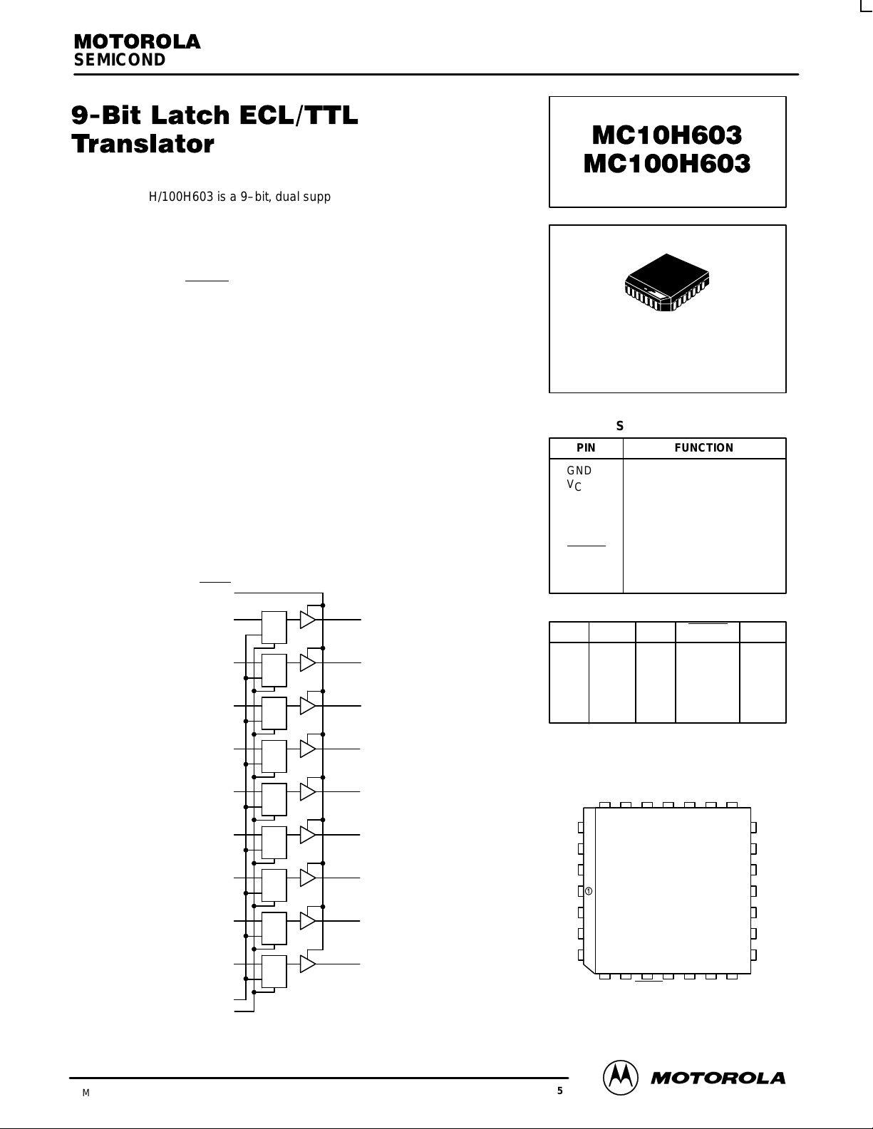
The MC10H/100H603 is a 9–bit, dual supply ECL to TTL translator.
Devices in the Motorola 9–bit translator series utilize the 28–lead PLCC for
optimal power pinning, signal flow–through and electrical performance.
The devices feature a 48 mA TTL output stage, and AC performance is
specified into both a 50 pF and 200 pF load capacitance. Latching is
controlled by Latch Enable (LEN), and Master Reset (MR) resets the
latches. A HIGH on OEECL
state. All control inputs are ECL level.
The 10H version is compatible with MECL 10H ECL logic levels. The
100H version is compatible with 100K levels.
• 9–Bit Ideal for Byte–Parity Applications
• 3–State TTL Outputs
• Flow–Through Configuration
• Extra TTL and ECL Power Pins to Minimize Switching Noise
• Dual Supply
• 6.0 ns Max Delay into 50 pF, 12 ns into 200 pF (all outputs switching)
• PNP TTL Inputs for Low Loading
sends the outputs into the high impedance
LOGIC SYMBOL
OEECL
D0
D1
D2
DQ
EN
DQ
EN
DQ
EN
Q0
Q1
Q2
FN SUFFIX
PLASTIC PACKAGE
CASE 776–02
PIN NAMES
PIN FUNCTION
GND
V
CCE
V
CCT
V
EE
D0–D8
Q0–Q8
OEECL
LEN
MR
TRUTH TABLE
D
L
H
X
X
X
TTL Ground (0 V)
ECL VCC (0 V)
TTL Supply (+5.0 V)
ECL Supply (–5.2/–4.5 V)
Data Inputs (ECL)
Data Outputs (TTL)
3-State Control (ECL)
Latch Enable (ECL)
Master Reset (ECL)
LEN
MR
L
L
H
X
X
L
L
L
H
X
OEECL
L
L
L
L
H
Q
L
H
Q
0
L
Z
3/93
Motorola, Inc. 1996
D3
D4
D5
D6
D7
D8
LEN
MR
DQ
EN
DQ
EN
DQ
EN
DQ
EN
DQ
EN
DQ
EN
2–311
Q3
Q4
Q5
Q6
Q7
Q8
Pinout: 28–Lead PLCC (Top View)
TTLECL
V
REV 5
Q4
Q3
CCT
Q2
GND
Q1
Q0
Q5 GND V
25 24 23 22 21 20 19
26
27
28
2
3
4
567891011
MR LEN OEECL
Q6 GND Q7 Q8
CCT
VEED0 D1 D2
18
D8
17
D7
16
V
CCE
D6
15
D5
14
D4
13
D3
12
Page 2
MC10H603 MC100H603
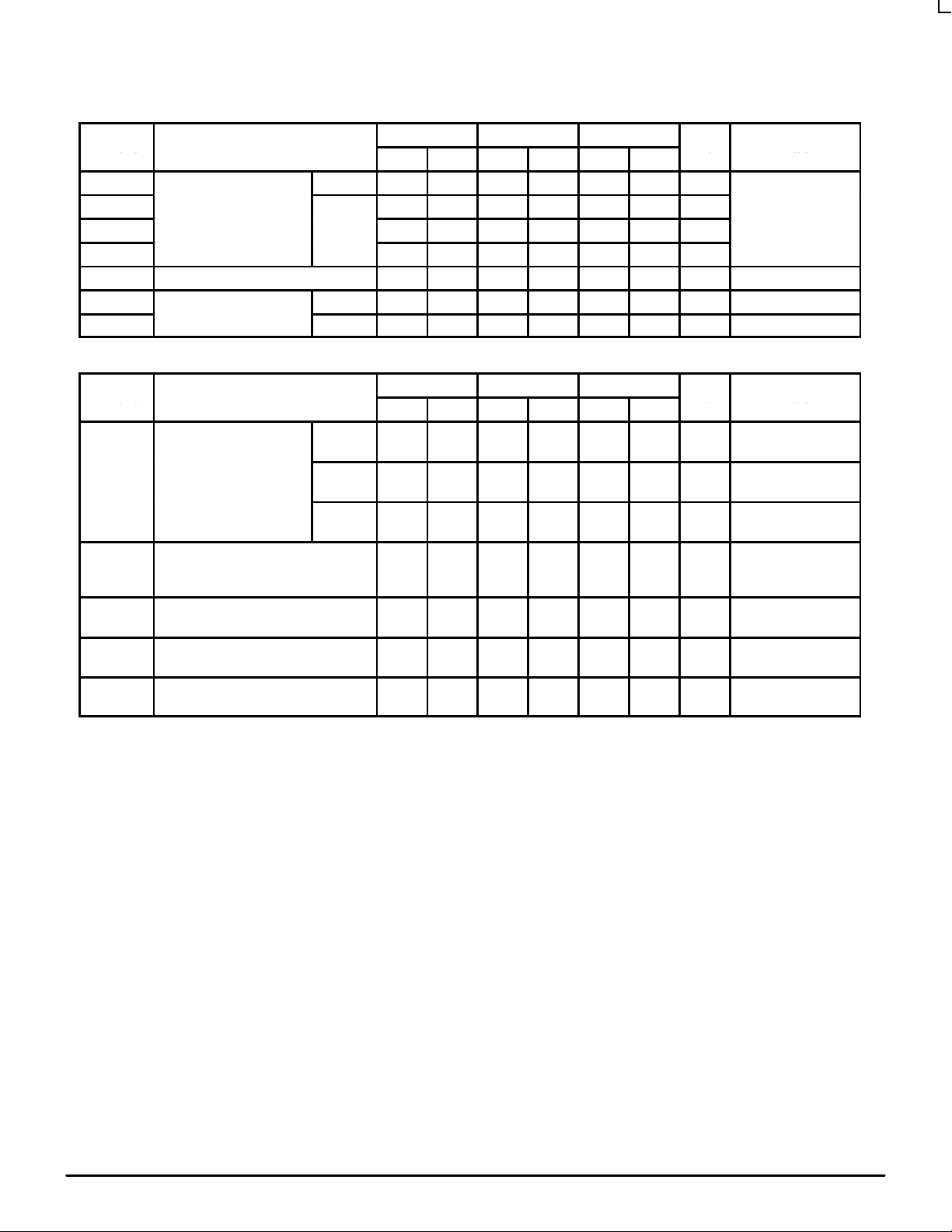
DC CHARACTERISTICS: V
Symbol Parameter
I
EE
I
CCH
I
CCL
I
CCZ
I
OS
I
OZH
I
OZL
Power Supply Current
Output Short Circuit Current –100 –225 –100 –225 –100 –225 mA V
Output Disable Current
AC CHARACTERISTICS: V
Symbol Parameter
t
PLH
t
PHL
t
s
t
h
tw(L)
t
PLZ
t
PHZ
t
PZL
t
PZH
t
R
t
F
Propagation Delay
to Output
Set–Up Time, D to LEN
Hold Time, D to LEN
LEN Pulse Width, LOW
Output Disable Time 2.5
Output Enable Time 2.0
Output Rise/Fall Time
1.0 V–2.0 V
CCT
CCT
= 5.0 V ± 10%; VEE = –5.2 V ± 5% (10H version); VEE = –4.2 V to –5.5 V (100H version)
0°C 25°C 75°C
Min Max Min Max Min Max
ECL –45 –63 –45 –64 –45 –68 mA
TTL
HIGH 50 50 50 µA V
LOW –50 –50 –50 µA V
= 5.0 V ± 10%; VEE = –5.2 V ± 5% (10H version); VEE = –4.2 V to –5.5 V (100H version)
D 3.0
LEN 3.5
MR 3.0
80 110 80 110 80 110 mA
80 110 80 110 80 110 mA
80 110 80 110 80 110 mA
0°C 25°C 75°C
Min Max Min Max Min Max
6.4
7.0
6.0
1.5
0.8
2.0
4.2
4.0
0.2
0.2
6.0
12
6.5
13
6.0
12
6.5
13
5.0
10
1.2
3.0
3.0
6.4
3.5
7.0
3.0
6.0
1.5
0.8
2.0
2.5
4.2
2.0
4.0
0.2
0.2
6.0
12
6.5
13
6.0
12
6.5
13
5.0
10
1.2
3.0
3.0
6.4
3.5
7.0
3.0
6.0
1.5
0.8
2.0
2.5
4.2
2.0
4.0
0.2
0.2
6.0
6.5
6.0
6.5
5.0
1.2
3.0
Unit Condition
Unit Condition
12
13
12
13
10
ns
ns
ns
ns
ns
ns
ns
ns
ns
ns
ns
ns
ns
ns
ns
OUT
OUT
OUT
CL = 50 pF
CL = 200 pF
CL = 50 pF
CL = 200 pF
CL = 50 pF
CL = 200 pF
CL = 50 pF
CL = 200 pF
CL = 50 pF
CL = 200 pF
CL = 50 pF
CL = 200 pF
= 0 V
= 2.7 V
= 0.5 V
MOTOROLA MECL Data
2–312
DL122 — Rev 6
Page 3

MC10H603 MC100H603
10H ECL DC CHARACTERISTICS: V
Symbol Parameter
I
IH
I
IL
V
IH
V
IL
Input HIGH Current
Input LOW Current
Input HIGH Voltage
Input LOW Voltage
100H ECL DC CHARACTERISTICS: V
Symbol Parameter
I
IH
I
IL
V
IH
V
IL
TTL DC CHARACTERISTICS: V
Symbol Parameter
V
IH
V
IL
I
IH
I
IL
V
IK
V
OH
V
OL
Input HIGH Current
Input LOW Current 0.5
Input HIGH Voltage
Input LOW Voltage
= 5.0 V ± 10%; VEE = –5.2 V ± 5% (10H version); VEE = –4.2 V to –5.5 V (100H version)
CCT
Input HIGH Voltage
Input LOW Voltage
Input HIGH Current 20
Input LOW Current –0.6 –0.6 –0.6 mA VIN = 0.5 V
Input Clamp Voltage –1.2 –1.2 –1.2 V IIN = –18 mA
Output HIGH Voltage 2.5
Output LOW Voltage 0.55 0.55 0.55 V IOL = 48 mA
= 5.0 V ± 10%; VEE = –5.2 V ± 5%
CCT
0°C 25°C 75°C
Min Max Min Max Min Max
0.5
–1170
–1950
= 5.0 V ± 10%; VEE = –4.2 V to –5.5 V
CCT
Min Max Min Max Min Max
–1165
–1810
Min Max Min Max Min Max
2.0
2.0
225
–840
–1480
0°C 25°C 75°C
–880
–1475
0°C 25°C 75°C
–1130
–1950
225
–1165
–1810
0.8
100
0.5
0.5
2.0
2.5
2.0
145
–810
–1480
145
–880
–1475
0.8
20
100
0.5
–1070
–1950
0.5
–1165
–1810
2.0
2.5
2.0
145 µA
–735
–1450
145 µA
–880
–1475
0.8
20
100
Unit Condition
µA
mV
Unit Condition
µA
mV
Unit Condition
V
V
µA VIN = 2.7 V
VIN = 7.0 V
V
IOH = –3.0 mA
V
IOH = –15 mA
DL122 — Rev 6
2–313 MOTOROLAMECL Data
Page 4

MC10H603 MC100H603
OUTLINE DIMENSIONS
FN SUFFIX
PLASTIC PLCC PACKAGE
CASE 776–02
ISSUE D
–L–
–N–
28 1
Z
C
G
G1
S
0.010 (0.250) N
L–M
T
Y BRK
0.007 (0.180) N
B
0.007 (0.180) N
U
M
T
L–M
M
S
S
S
L–M
T
S
D
Z
–M–
W
D
V
0.010 (0.250) N
G1X
S
T
L–M
S
S
VIEW D–D
A
0.007 (0.180) N
0.007 (0.180) N
R
E
M
M
S
L–M
T
L–M
T
S
S
S
H
0.007 (0.180) N
M
T
L–M
S
S
K1
0.004 (0.100)
SEATING
J
–T–
PLANE
VIEW S
S
S
K
VIEW S
0.007 (0.180) N
F
M
S
L–M
T
S
NOTES:
1. DATUMS –L–, –M–, AND –N– DETERMINED
WHERE TOP OF LEAD SHOULDER EXITS
PLASTIC BODY AT MOLD PARTING LINE.
2. DIMENSION G1, TRUE POSITION TO BE
MEASURED AT DA TUM –T–, SEATING PLANE.
3. DIMENSIONS R AND U DO NOT INCLUDE
MOLD FLASH. ALLOWABLE MOLD FLASH IS
0.010 (0.250) PER SIDE.
4. DIMENSIONING AND TOLERANCING PER
ANSI Y14.5M, 1982.
5. CONTROLLING DIMENSION: INCH.
6. THE PACKAGE TOP MAY BE SMALLER THAN
THE PACKAGE BOTTOM BY UP TO 0.012
(0.300). DIMENSIONS R AND U ARE
DETERMINED AT THE OUTERMOST
EXTREMES OF THE PLASTIC BODY
EXCLUSIVE OF MOLD FLASH, TIE BAR
BURRS, GATE BURRS AND INTERLEAD
FLASH, BUT INCLUDING ANY MISMATCH
BETWEEN THE TOP AND BOTTOM OF THE
PLASTIC BODY.
7. DIMENSION H DOES NOT INCLUDE DAMBAR
PROTRUSION OR INTRUSION. THE DAMBAR
PROTRUSION(S) SHALL NOT CAUSE THE H
DIMENSION TO BE GREATER THAN 0.037
(0.940). THE DAMBAR INTRUSION(S) SHALL
NOT CAUSE THE H DIMENSION TO BE
SMALLER THAN 0.025 (0.635).
DIM MIN MAX MIN MAX
A 0.485 0.495 12.32 12.57
B 0.485 0.495 12.32 12.57
C 0.165 0.180 4.20 4.57
E 0.090 0.1 10 2.29 2.79
F 0.013 0.019 0.33 0.48
G 0.050 BSC 1.27 BSC
H 0.026 0.032 0.66 0.81
J 0.020 ––– 0.51 –––
K 0.025 ––– 0.64 –––
R 0.450 0.456 11.43 11.58
U 0.450 0.456 11.43 11.58
V 0.042 0.048 1.07 1.21
W 0.042 0.048 1.07 1.21
X 0.042 0.056 1.07 1.42
Y ––– 0.020 ––– 0.50
Z 2 10 2 10
____
G1 0.410 0.430 10.42 10.92
K1 0.040 ––– 1.02 –––
MILLIMETERSINCHES
MOTOROLA MECL Data
2–314
DL122 — Rev 6
Page 5

MC10H603 MC100H603
Motorola reserves the right to make changes without further notice to any products herein. Motorola makes no warranty , representation or guarantee regarding
the suitability of its products for any particular purpose, nor does Motorola assume any liability arising out of the application or use of any product or circuit, and
specifically disclaims any and all liability, including without limitation consequential or incidental damages. “T ypical” parameters which may be provided in Motorola
data sheets and/or specifications can and do vary in different applications and actual performance may vary over time. All operating parameters, including “Typicals”
must be validated for each customer application by customer’s technical experts. Motorola does not convey any license under its patent rights nor the rights of
others. Motorola products are not designed, intended, or authorized for use as components in systems intended for surgical implant into the body, or other
applications intended to support or sustain life, or for any other application in which the failure of the Motorola product could create a situation where personal injury
or death may occur. Should Buyer purchase or use Motorola products for any such unintended or unauthorized application, Buyer shall indemnify and hold Motorola
and its officers, employees, subsidiaries, affiliates, and distributors harmless against all claims, costs, damages, and expenses, and reasonable attorney fees
arising out of, directly or indirectly, any claim of personal injury or death associated with such unintended or unauthorized use, even if such claim alleges that
Motorola was negligent regarding the design or manufacture of the part. Motorola and are registered trademarks of Motorola, Inc. Motorola, Inc. is an Equal
Opportunity/Affirmative Action Employer.
How to reach us:
USA/EUROPE /Locations Not Listed: Motorola Literature Distribution; JAP AN: Nippon Motorola Ltd.; Tatsumi–SPD–JLDC, 6F Seibu–Butsuryu–Center,
P.O. Box 20912; Phoenix, Arizona 85036. 1–800–441–2447 or 602–303–5454 3–14–2 Ta tsumi Koto–Ku, Tokyo 135, Japan. 03–81–3521–8315
MFAX: RMF AX0@email.sps.mot.com – T OUCHTONE 602–244–6609 ASIA/PACIFIC: Motorola Semiconductors H.K. Ltd.; 8B Tai Ping Industrial Park,
INTERNET: http://Design–NET .com 51 Ting Kok Road, Tai Po, N.T., Hong Kong. 852–26629298
MC10H603/D
DL122 — Rev 6
◊
2–315 MOTOROLAMECL Data
*MC10H603/D*
 Loading...