

Page 1
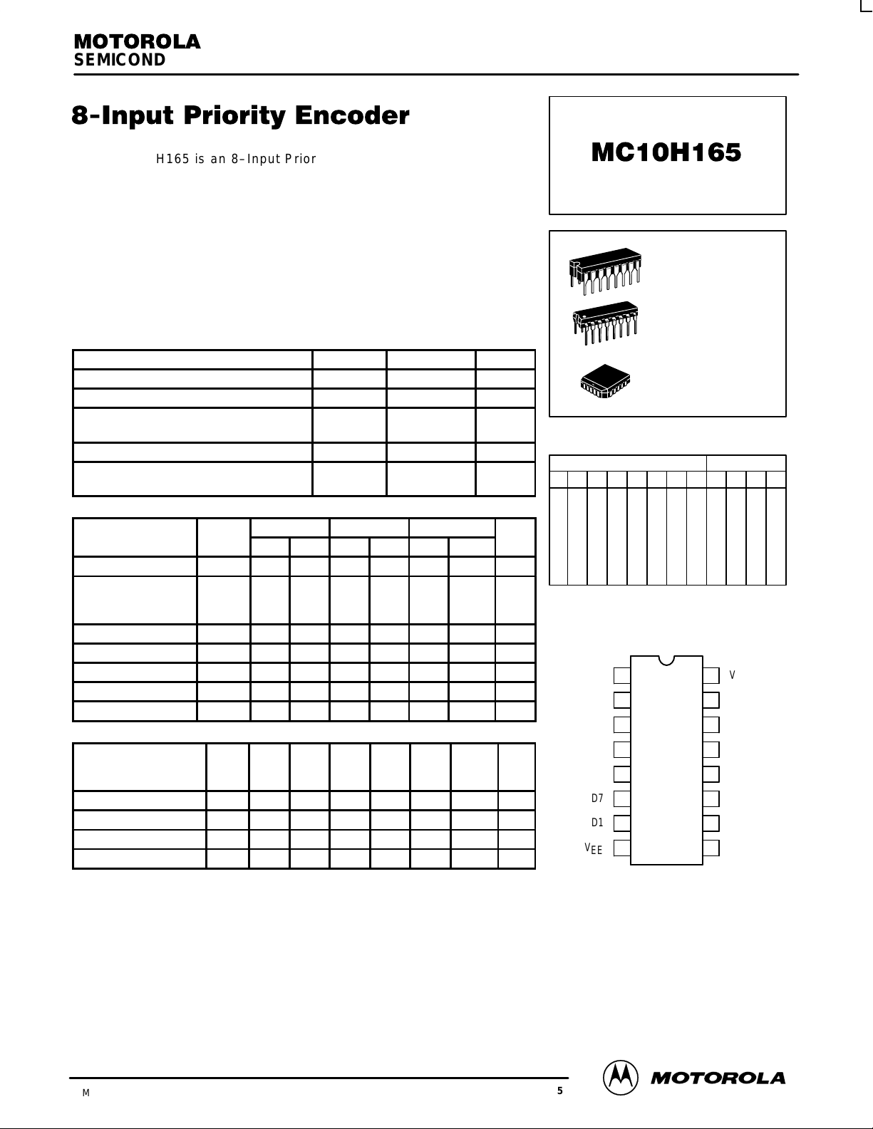
SEMICONDUCTOR TECHNICAL DATA
The MC10H165 is an 8–Input Priority Encoder. This 10H part is a
functional/pinout duplication of the standard MECL 10K family part, with 100%
improvement in propagation delay, and no increases in power–
supply current.
• Propagation Delay, Data–to–Output, 2.2 ns Typical
• Improved Noise Margin 150 mV (Over Operating Voltage and
Temperature Range)
• Voltage Compensated
• MECL 10K–Compatible
MAXIMUM RATINGS
Characteristic Symbol Rating Unit
Power Supply (VCC = 0) V
Input Voltage (VCC = 0) V
Output Current— Continuous
I
— Surge
Operating Temperature Range T
Storage Temperature Range— Plastic
T
— Ceramic
EE
I
out
A
stg
–8.0 to 0 Vdc
0 to V
EE
50
100
0 to +75 °C
–55 to +150
–55 to +165
Vdc
mA
°C
ELECTRICAL CHARACTERISTICS (VEE = –5.2 V ±5%) (See Note)
0° 25° 75°
Characteristic Symbol Min Max Min Max Min Max Unit
Power Supply Current I
Input Current High
Pin 4
Data Inputs
Input Current Low I
High Output Voltage V
Low Output Voltage V
High Input Voltage V
Low Input Voltage V
I
E
inH
inL
OH
OL
IH
— 144 — 131 — 144 mA
——510
600——
320
370——
0.5 — 0.5 — 0.3 — µA
–1.02 –0.84 –0.98 –0.81 –0.92 –0.735 Vdc
–1.95 –1.63 –1.95 –1.63 –1.95 –1.60 Vdc
–1.17 –0.84 –1.13 –0.81 –1.07 –0.735 Vdc
–1.95 –1.48 –1.95 –1.48 –1.95 –1.45 Vdc
IL
µAdc
320
370
AC PARAMETERS
Propagation Delay
Data Input → Output
Clock Input → Output
Set–up Time t
Hold Time t
Rise Time t
Fall Time t
NOTE:
Each MECL 10H series circuit has been designed to meet the dc specifications shown in the test table,
after thermal equilibrium has been established. The circuit is in a test socket or mounted on a printed circuit
board and transverse air flow greater than 500 Ifpm is maintained. Outputs are terminated through a
50–ohm resistor to –2.0 volts.
t
pd
0.7
3.4
0.7
3.4
0.7
2.2
0.7
3.0 — 3.0 — 3.0 — ns
set
0.5 — 0.5 — 0.5 — ns
hold
0.5 2.4 0.5 2.4 0.5 2.4 ns
r
0.5 2.4 0.5 2.4 0.5 2.4 ns
f
2.2
0.7
0.7
3.4
2.2
ns
L SUFFIX
CERAMIC PACKAGE
CASE 620–10
P SUFFIX
PLASTIC PACKAGE
CASE 648–08
FN SUFFIX
PLCC
CASE 775–02
TRUTH TABLE
DATA INPUTS OUTPUTS
D0
D1
D2
D3
D4
D5
D6
D7
Q3
Q2
Q1
H
X
X
X
X
X
X
X
H
L
L
H
X
X
X
X
X
L
L
H
X
L
L
L
L
L
L
L
L
L
L
L
L
X
L
H
X
L
L
H
L
L
L
L
L
L
L
L
L
L
L
L
X
X
X
X
X
X
X
X
X
X
H
X
X
L
H
X
L
L
H
L
L
L
DIP
PIN ASSIGNMENT
V
CC1
Q1
Q0
CLOCK
D0
D7
D1
V
EE
Pin assignment is for Dual–in–Line Package.
For PLCC pin assignment, see the Pin Conversion
T ables on page 6–11 of the Motorola MECL Data
1
2
3
4
5
6
7
8
Book (DL122/D).
16
15
14
13
12
11
10
9
L
H
L
L
H
L
H
H
L
H
H
H
L
H
H
L
H
H
H
H
H
H
L
L
L
V
CC2
Q2
Q3
D2
D5
D4
D3
D6
Q0
L
H
L
H
L
H
L
H
L
3/93
Motorola, Inc. 1996
2–261
REV 5
Page 2
MC10H165
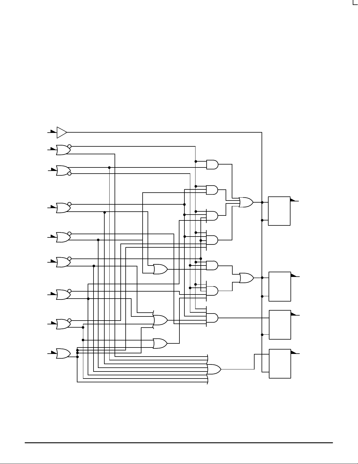
8–INPUT PRIORITY ENCODER
The MC10H165 is a device designed to encode eight
inputs to a binary coded output. The output code is that
of the highest order input. Any input of lower priority is
ignored. Each output incorporates a latch allowing
synchronous operation. When the clock is low the outputs
follow the inputs and latch when the clock goes high. This
device is very useful for a variety of applications in
checking system status in control processors, peripheral
C 4
D0 5
D1 7
D2 13
The input is active when high, (e.g., the three binary
outputs are low when input D0 is high). The Q3 output is
high when any input is high. This allows direct extension
into another priority encoder when more than eight inputs
are necessary. The MC10H165 can also be used to
develop binary codes from random logic inputs, for
addressing ROMs, RAMs, or for multiplexing data.
LOGIC DIAGRAM
controllers, and testing systems.
V
V
VEE= PIN 8.
CC1
CC2
= PIN 1
= PIN 16
3 Q0
D3 10
D4 11
D5 12
D6 9
D7 6
Numbers at ends of terminals denote pin numbers for L and P packages.
2 Q1
15 Q2
14 Q3
MOTOROLA MECL Data
2–262
DL122 — Rev 6
Page 3

APPLICATION INFORMATION
MC10H165
A typical application of the MC10H165 is the decoding
of system status on a priority basis. A 64–line priority
encoder is shown in the figure below. System status lines
are connected to this encoder such that, when a given
condition exists, the respective input will be at a logic high
level. This scheme will select the one of 64 different
64–LINE PRIORITY ENCODER
ZZZ
MC10H164 MC10H164
X0 X7. . . . . . . A B C X0 X7. . . . . . . A B C
System
Clock
Highest
Priority
Input
Lowest
Priority
Input
1/2 MC10H101
C
D0
MC10H165MC10H165MC10H165MC10H165MC10H165MC10H165MC10H165MC10H165
D7
C
D0
D7
C
D0
D7
C
D0
D7
C
D0
D7
C
D0
D7
C
D0
D7
C
D0
D7
MC10H164
X0 X7. . . . . . . A B C
Q0
Q1
Q2
Q3
Q0
Q1
Q2
Q3
Q0
Q1
Q2
Q3
Q0
Q1
Q2
Q3
Q0
Q1
Q2
Q3
Q0
Q1
Q2
Q3
Q0
Q1
Q2
Q3
Q0
Q1
Q2
Q3
system conditions, as represented at the encoder inputs,
which has priority in determining the next system
operation to be performed. The binary code showing the
address of the highest priority input present will appear at
the encoder outputs to control other system logic
functions.
LSB
Six bit output
word yielding
number of
highest priority
channel present
at input
C
Q0
D0
Q1
Q2
D7
MSB
DL122 — Rev 6
2–263 MOTOROLAMECL Data
Page 4

MC10H165
OUTLINE DIMENSIONS
FN SUFFIX
PLASTIC PLCC PACKAGE
CASE 775–02
ISSUE C
–L–
20 1
Z
C
G
G1
0.010 (0.250) N
S
T
–N–
L–M
S
Y BRK
–M–
W
V
A
0.007 (0.180) N
0.007 (0.180) N
R
E
0.004 (0.100)
J
PLANE
SEATING
–T–
VIEW S
S
0.007 (0.180) N
B
0.007 (0.180) N
U
M
S
L–M
T
M
S
S
L–M
T
S
D
Z
D
X
0.010 (0.250) N
G1
S
S
L–M
T
S
VIEW D–D
M
M
S
L–M
T
L–M
T
S
S
S
0.007 (0.180) N
H
M
S
L–M
T
S
K1
K
0.007 (0.180) N
F
M
S
L–M
T
S
VIEW S
NOTES:
1. DATUMS –L–, –M–, AND –N– DETERMINED
WHERE TOP OF LEAD SHOULDER EXITS PLASTIC
BODY AT MOLD PARTING LINE.
2. DIMENSION G1, TRUE POSITION TO BE
MEASURED AT DA TUM –T–, SEATING PLANE.
3. DIMENSIONS R AND U DO NOT INCLUDE MOLD
FLASH. ALLOWABLE MOLD FLASH IS 0.010 (0.250)
PER SIDE.
4. DIMENSIONING AND TOLERANCING PER ANSI
Y14.5M, 1982.
5. CONTROLLING DIMENSION: INCH.
6. THE PACKAGE TOP MAY BE SMALLER THAN THE
PACKAGE BOTTOM BY UP TO 0.012 (0.300).
DIMENSIONS R AND U ARE DETERMINED AT THE
OUTERMOST EXTREMES OF THE PLASTIC BODY
EXCLUSIVE OF MOLD FLASH, TIE BAR BURRS,
GATE BURRS AND INTERLEAD FLASH, BUT
INCLUDING ANY MISMATCH BETWEEN THE TOP
AND BOTTOM OF THE PLASTIC BODY.
7. DIMENSION H DOES NOT INCLUDE DAMBAR
PROTRUSION OR INTRUSION. THE DAMBAR
PROTRUSION(S) SHALL NOT CAUSE THE H
DIMENSION TO BE GREATER THAN 0.037 (0.940).
THE DAMBAR INTRUSION(S) SHALL NOT CAUSE
THE H DIMENSION TO BE SMALLER THAN 0.025
(0.635).
MOTOROLA MECL Data
DIM MIN MAX MIN MAX
A 0.385 0.395 9.78 10.03
B 0.385 0.395 9.78 10.03
C 0.165 0.180 4.20 4.57
E 0.090 0.110 2.29 2.79
F 0.013 0.019 0.33 0.48
G 0.050 BSC 1.27 BSC
H 0.026 0.032 0.66 0.81
J 0.020 ––– 0.51 –––
K 0.025 ––– 0.64 –––
R 0.350 0.356 8.89 9.04
U 0.350 0.356 8.89 9.04
V 0.042 0.048 1.07 1.21
W 0.042 0.048 1.07 1.21
X 0.042 0.056 1.07 1.42
Y ––– 0.020 ––– 0.50
Z 2 10 2 10
____
G1 0.310 0.330 7.88 8.38
K1 0.040 ––– 1.02 –––
2–264
MILLIMETERSINCHES
DL122 — Rev 6
Page 5

OUTLINE DIMENSIONS
CERAMIC DIP PACKAGE
–A–
16 9
–B–
18
C
–T–
SEATING
PLANE
E
F
G
16 PLD
0.25 (0.010) T
M
–A–
916
B
18
F
C
S
H
G
D
16 PL
0.25 (0.010) T
K
M
K
N
S
A
PLASTIC DIP PACKAGE
SEATING
–T–
PLANE
M
A
L SUFFIX
CASE 620–10
ISSUE V
L
M
16 PLJ
0.25 (0.010) T
P SUFFIX
CASE 648–08
ISSUE R
L
J
MC10H165
NOTES:
1. DIMENSIONING AND TOLERANCING PER
ANSI Y14.5M, 1982.
2. CONTROLLING DIMENSION: INCH.
3. DIMENSION L TO CENTER OF LEAD WHEN
FORMED PARALLEL.
4. DIMENSION F MAY NARROW TO 0.76 (0.030)
WHERE THE LEAD ENTERS THE CERAMIC
BODY.
DIM MIN MAX MIN MAX
A 0.750 0.785 19.05 19.93
B 0.240 0.295 6.10 7.49
C ––– 0.200 ––– 5.08
D 0.015 0.020 0.39 0.50
E 0.050 BSC 1.27 BSC
F 0.055 0.065 1.40 1.65
G 0.100 BSC 2.54 BSC
H 0.008 0.015 0.21 0.38
K 0.125 0.170 3.18 4.31
M
S
B
NOTES:
1. DIMENSIONING AND TOLERANCING PER ANSI
2. CONTROLLING DIMENSION: INCH.
3. DIMENSION L TO CENTER OF LEADS WHEN
4. DIMENSION B DOES NOT INCLUDE MOLD FLASH.
5. ROUNDED CORNERS OPTIONAL.
M
L 0.300 BSC 7.62 BSC
M 0 15 0 15
____
N 0.020 0.040 0.51 1.01
Y14.5M, 1982.
FORMED PARALLEL.
DIM MIN MAX MIN MAX
A 0.740 0.770 18.80 19.55
B 0.250 0.270 6.35 6.85
C 0.145 0.175 3.69 4.44
D 0.015 0.021 0.39 0.53
F 0.040 0.70 1.02 1.77
G 0.100 BSC 2.54 BSC
H 0.050 BSC 1.27 BSC
J 0.008 0.015 0.21 0.38
K 0.110 0.130 2.80 3.30
L 0.295 0.305 7.50 7.74
M 0 10 0 10
S 0.020 0.040 0.51 1.01
MILLIMETERSINCHES
MILLIMETERSINCHES
____
Motorola reserves the right to make changes without further notice to any products herein. Motorola makes no warranty , representation or guarantee regarding
the suitability of its products for any particular purpose, nor does Motorola assume any liability arising out of the application or use of any product or circuit, and
specifically disclaims any and all liability, including without limitation consequential or incidental damages. “T ypical” parameters which may be provided in Motorola
data sheets and/or specifications can and do vary in different applications and actual performance may vary over time. All operating parameters, including “Typicals”
must be validated for each customer application by customer’s technical experts. Motorola does not convey any license under its patent rights nor the rights of
others. Motorola products are not designed, intended, or authorized for use as components in systems intended for surgical implant into the body, or other
applications intended to support or sustain life, or for any other application in which the failure of the Motorola product could create a situation where personal injury
or death may occur. Should Buyer purchase or use Motorola products for any such unintended or unauthorized application, Buyer shall indemnify and hold Motorola
and its officers, employees, subsidiaries, affiliates, and distributors harmless against all claims, costs, damages, and expenses, and reasonable attorney fees
arising out of, directly or indirectly, any claim of personal injury or death associated with such unintended or unauthorized use, even if such claim alleges that
Motorola was negligent regarding the design or manufacture of the part. Motorola and are registered trademarks of Motorola, Inc. Motorola, Inc. is an Equal
Opportunity/Affirmative Action Employer.
How to reach us:
USA/EUROPE/Locations Not Listed: Motorola Literature Distribution; JAPAN: Nippon Motorola Ltd.; Tatsumi–SPD–JLDC, 6F Seibu–Butsuryu–Center,
P.O. Box 20912; Phoenix, Arizona 85036. 1–800–441–2447 or 602–303–5454 3–14–2 Tatsumi Koto–Ku, Tokyo 135, Japan. 03–81–3521–8315
MFAX: RMF AX0@email.sps.mot.com – T OUCHTONE 602–244–6609 ASIA/PACIFIC: Motorola Semiconductors H.K. Ltd.; 8B Tai Ping Industrial Park,
INTERNET: http://Design–NET .com 51 Ting Kok Road, Tai Po, N.T., Hong Kong. 852–26629298
MC10H165/D
DL122 — Rev 6
◊
2–265 MOTOROLAMECL Data
*MC10H165/D*
 Loading...