

Page 1
MC10EP89
Coaxial Cable Driver
The MC10EP89 is a differential fanout gate specifically designed to
drive coaxial cables. The device is especially useful in digital video
broadcasting applications; for this application, since the system is
polarity free, each output can be used as an independent driver. The
driver produces swings 70% larger than a standard ECL output. When
driving a coaxial cable, proper termination is required at both ends of
the line to minimize signal loss. The 1.6 (5V) and 1.4V (3.3V) swing
allow for termination at both ends of the cable, while maintaining a
800mV (5V) and 700mV (3.3V) swing at the receiving end of the
cable. Because of the larger output swings, the device cannot be
terminated into the standard VCC–2.0V. All of the DC parameters are
tested with a 50Ω to VCC–3.0V load. The driver accepts a standard
differential ECL input and can run off of the digital video broadcast
standard –5.0V supply .
http://onsemi.com
8
1
SO–8
D SUFFIX
CASE 751
• 310ps T ypical Propagation Delay
• 3.0 GHz T ypical Toggle Frequency
• 1.6V (5V) and 1.4V (3.3V) Swing
• PECL mode: 3.0V to 5.5V V
• ECL mode: 0V V
with VEE = –3.0V to –5.5V
CC
with VEE = 0V
CC
• Internal Input Resistors: Pulldown on D, Pulldown and Pullup on D
• Q Output will default LOW with inputs open or at V
EE
• ESD Protection: >4KV HBM, >200V MM
• New Differential Input Common Mode Range
• Moisture Sensitivity Level 1, Indefinite Time Out of Drypack
• Flammability Rating: UL–94 code V–0 @ 1/8”,
Oxygen Index 28 to 34
• Transistor Count = 152 devices
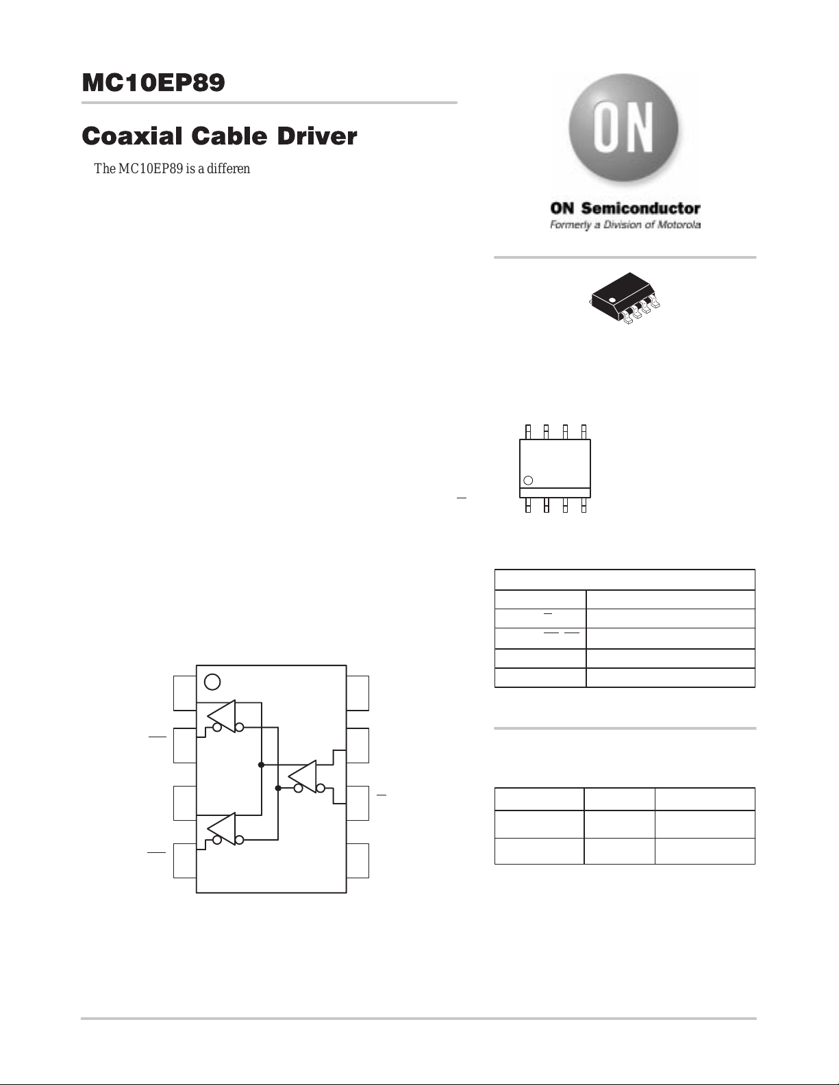
Q0
Q0
Q1
1
2
3
78D
6
V
CC
D
MARKING DIAGRAM
8
HEP89
ALYW
1
*For additional information, see Application Note
AND8002/D
PIN DESCRIPTION
PIN
D, D
Q0, Q1, Q0, Q1 ECL Data Outputs
V
CC
V
EE
ORDERING INFORMATION
Device Package Shipping
MC10EP89D SOIC 98 Units/Rail
A = Assembly Location
L = W afer Lot
Y = Year
W = Work Week
FUNCTION
ECL Data Inputs
Positive Supply
Negative, 0 Supply
45
Q1
Figure 1. 8–Lead Pinout (Top View) and Logic Diagram
Semiconductor Components Industries, LLC, 1999
December, 1999 – Rev. 1
V
EE
1 Publication Order Number:
MC10EP89DR2 SOIC 2500 Tape & Reel
MC10EP89/D
Page 2
MC10EP89
MAXIMUM RATINGS*
Symbol Parameter Value Unit
V
EE
V
CC
V
I
V
I
I
out
T
A
T
stg
θ
JA
θ
JC
T
sol
* Maximum Ratings are those values beyond which damage to the device may occur.
Power Supply (VCC = 0V) –6.0 to 0 VDC
Power Supply (VEE = 0V) 6.0 to 0 VDC
Input Voltage (VCC = 0V, VI not more negative than VEE) –6.0 to 0 VDC
Input Voltage (VEE = 0V, VI not more positive than VCC) 6.0 to 0 VDC
Output Current Continuous
Surge
Operating Temperature Range –40 to +85 °C
Storage Temperature –65 to +150 °C
Thermal Resistance (Junction–to–Ambient) Still Air
500lfpm
Thermal Resistance (Junction–to–Case) 41 to 44 ± 5% °C/W
Solder Temperature (<2 to 3 Seconds: 245°C desired) 265 °C
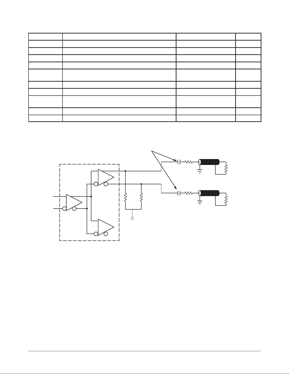
DC BLOCKING CAPACITORS
75Ω
50
100
190
130
75Ω COAX
mA
°C/W
EP89
0.1µF
150Ω 150Ω
V
EE
0.1µF
Figure 2. EP89 T ermination Configuration
75Ω
75Ω
75Ω COAX
75Ω
http://onsemi.com
2
Page 3
MC10EP89
DC CHARACTERISTICS, ECL/LVECL (VCC = 0V; VEE = –3.3 ± 0.01V) (Note 4.)
–40°C 25°C 85°C
Symbol Characteristic Min Typ Max Min Typ Max Min Typ Max Unit
IEE
V
OH
V
OL
V
IH
V
IL
V
IHCMR
I
IH
I
IL
NOTE: 10EP circuits are designed to meet the DC specifications shown in the above table after thermal equilibrium has been established. The
1. VCC = 0V, VEE = –3.3V , all other pins floating.
2. All loading with 50 ohms to VCC–3.0 volts.
3. V
4. Input and output parameters vary 1:1 with VCC.
Power Supply Current
(Note 1.)
Output HIGH Voltage
(Note 2.)
Output LOW Voltage
(Note 2.)
Input HIGH Voltage
Single Ended
Input LOW Voltage
Single Ended
Input HIGH Voltage Common Mode
Range (Note 3.)
Input HIGH Current 150 150 150 µA
Input LOW Current D
circuit is in a test socket or mounted on a printed circuit board and transverse airflow greater than 500lfpm is maintained.
min varies 1:1 with VEE, max varies 1:1 with VCC.
IHCMR
D
22 28 34 24 32 38 28 34 40 mA
–1220 –1120 –1020 –1150 –1050 –950 –1075 –975 –875 mV
–2680 –2580 –2480 –2670 –2570 –2470 –2630 –2530 –2430 mV
–1230 –890 –1130 –810 –1060 –720 mV
–1950 –1500 –1950 –1480 –1950 –1445 mV
–1.3 0.0 –1.3 0.0 –1.3 0.0 V
0.5
–150
0.5
–150
0.5
–150
µA
DC CHARACTERISTICS, ECL/LVECL (VCC = 0V; VEE = –5.2 ± 0.01V) (Note 8.)
–40°C 25°C 85°C
Symbol Characteristic Min Typ Max Min Typ Max Min Typ Max Unit
IEE
V
OH
V
OL
V
IH
V
IL
V
IHCMR
I
IH
I
IL
NOTE: 10EP circuits are designed to meet the DC specifications shown in the above table after thermal equilibrium has been established. The
5. VCC = 0V, VEE = –5.2V , all other pins floating.
6. All loading with 50 ohms to VCC–3.0 volts.
7. V
8. Input and output parameters vary 1:1 with VCC.
Power Supply Current
(Note 5.)
Output HIGH Voltage
(Note 6.)
Output LOW Voltage
(Note 6.)
Input HIGH Voltage
Single Ended
Input LOW Voltage
Single Ended
Input HIGH Voltage Common Mode
Range (Note 7.)
Input HIGH Current 150 150 150 µA
Input LOW Current D
circuit is in a test socket or mounted on a printed circuit board and transverse airflow greater than 500lfpm is maintained.
min varies 1:1 with VEE, max varies 1:1 with VCC.
IHCMR
D
25 32 39 28 35 42 31 38 45 mA
–1220 –1120 –1020 –1150 –1050 –950 –1075 –975 –875 mV
–2950 –2800 –2650 –2950 –2850 –2650 –2950 –2800 –2650 mV
–1230 –890 –1130 –810 –1060 –720 mV
–1950 –1500 –1950 –1480 –1950 –1445 mV
–3.2 0.0 –3.2 0.0 –3.2 0.0 V
0.5
–150
0.5
–150
0.5
–150
µA
http://onsemi.com
3
Page 4

MC10EP89
DC CHARACTERISTICS, LVPECL (VCC = 3.3V ± 0.01V, VEE = 0V) (Note 12.)
–40°C 25°C 85°C
Symbol Characteristic Min Typ Max Min Typ Max Min Typ Max Unit
IEE
V
OH
V
OL
V
IH
V
IL
V
IHCMR
I
IH
I
IL
NOTE: 10EP circuits are designed to meet the DC specifications shown in the above table after thermal equilibrium has been established. The
9. VCC = 3.3V, VEE = 0V, all other pins floating.
10.All loading with 50 ohms to VCC–3.0 volts.
11. V
12.Input and output parameters vary 1:1 with VCC.
Power Supply Current
(Note 9.)
Output HIGH Voltage
(Note 10.)
Output LOW Voltage
(Note 10.)
Input HIGH Voltage
Single Ended
Input LOW Voltage
Single Ended
Input HIGH Voltage Common Mode
Range (Note 11.)
Input HIGH Current 150 150 150 µA
Input LOW Current D
circuit is in a test socket or mounted on a printed circuit board and transverse airflow greater than 500lfpm is maintained.
min varies 1:1 with VEE, max varies 1:1 with VCC.
IHCMR
D
22 28 34 24 32 38 28 34 40 mA
2080 2180 2280 2150 2250 2350 2225 2325 2425 mV
620 720 820 630 730 830 670 770 870 mV
2070 2410 2170 2490 2240 2580 mV
1350 1800 1350 1820 1350 1855 mV
2.0 3.3 2.0 3.3 2.0 3.3 V
0.5
–150
0.5
–150
0.5
–150
µA
DC CHARACTERISTICS, PECL (VCC = 5.0V ± 0.5V, VEE = 0V) (Note 16.)
–40°C 25°C 85°C
Symbol Characteristic Min Typ Max Min Typ Max Min Typ Max Unit
IEE
V
OH
V
OL
V
IH
V
IL
V
IHCMR
I
IH
I
IL
NOTE: 10EP circuits are designed to meet the DC specifications shown in the above table after thermal equilibrium has been established. The
13.VCC = 5.0V, VEE = 0V, all other pins floating.
14.All loading with 50 ohms to VCC–3.0 volts.
15.V
16.Input and output parameters vary 1:1 with VCC.
Power Supply Current
(Note 13.)
Output HIGH Voltage
(Note 14.)
Output LOW Voltage
(Note 14.)
Input HIGH Voltage
Single Ended
Input LOW Voltage
Single Ended
Input HIGH Voltage Common Mode
Range (Note 15.)
Input HIGH Current 150 150 150 µA
Input LOW Current D
circuit is in a test socket or mounted on a printed circuit board and transverse airflow greater than 500lfpm is maintained.
min varies 1:1 with VEE, max varies 1:1 with VCC.
IHCMR
D
27 34 41 30 37 44 32 39 46 mA
3780 3880 3980 3850 3950 4050 3925 4025 4125 mV
2075 2225 2375 2060 2210 2360 2090 2240 2390 mV
3770 4110 3870 4190 3940 4280 mV
3050 3500 3050 3520 3050 3555 mV
2.0 5.0 2.0 5.0 2.0 5.0 V
0.5
–150
0.5
–150
0.5
–150
µA
http://onsemi.com
4
Page 5

MC10EP89
AC CHARACTERISTICS (VCC = 0V; VEE = –3.0V to –5.5V) or (VCC = 3.0V to 5.5V; VEE =
–40°C 25°C 85°C
Symbol Characteristic Min Typ Max Min Typ Max Min Typ Max Unit
f
max
t
PLH
t
PHL
t
SKEW
t
JITTER
V
PP
t
r
t
f
17.F
18.Skew is measured between outputs under identical transitions. Duty cycle skew is defined only for differential operation when the delays
are measured from the cross point of the inputs to the cross point of the outputs.
19.VIL must not go below VCC – 3V.
Maximum Toggle
Frequency (Note 17.)
,
Propagation Delay to
Output Differential
Duty Cycle Skew (Note 18.) 5.0 20 5.0 20 5.0 20 ps
Cycle–to–Cycle Jitter TBD TBD TBD ps
Input Voltage Swing (Diff.)
(Note 19.)
Output Rise/Fall Times Q
(20% – 80%)
guaranteed for functionality only.
max
200 280 380 220 310 400 250 330 420 ps
150 800 1200 150 800 1200 150 800 1200 mV
120 230 380 130 250 410 150 270 430 ps
3.0 GHz
0V)
http://onsemi.com
5
Page 6

MC10EP89
P ACKAGE DIMENSIONS
SO–8
D SUFFIX
PLASTIC SOIC PACKAGE
CASE 751–06
ISSUE T
C
A
E
B
A1
D
58
0.25MB
1
H
4
e
M
h
X 45
_
q
C
A
SEATING
PLANE
0.10
L
B
SS
A0.25MCB
NOTES:
1. DIMENSIONING AND TOLERANCING PER ASME
Y14.5M, 1994.
2. DIMENSIONS ARE IN MILLIMETER.
3. DIMENSION D AND E DO NOT INCLUDE MOLD
PROTRUSION.
4. MAXIMUM MOLD PROTRUSION 0.15 PER SIDE.
5. DIMENSION B DOES NOT INCLUDE DAMBAR
PROTRUSION. ALLOWABLE DAMBAR
PROTRUSION SHALL BE 0.127 TOTAL IN EXCESS
OF THE B DIMENSION AT MAXIMUM MATERIAL
CONDITION.
MILLIMETERS
DIM MIN MAX
A 1.35 1.75
A1 0.10 0.25
B 0.35 0.49
C 0.19 0.25
D 4.80 5.00
E
3.80 4.00
1.27 BSCe
H 5.80 6.20
h
0.25 0.50
L 0.40 1.25
0 7
q
__
http://onsemi.com
6
Page 7

Notes
MC10EP89
http://onsemi.com
7
Page 8

MC10EP89
ON Semiconductor and are trademarks of Semiconductor Components Industries, LLC (SCILLC). SCILLC reserves the right to make changes
without further notice to any products herein. SCILLC makes no warranty , representation or guarantee regarding the suitability of its products for any particular
purpose, nor does SCILLC assume any liability arising out of the application or use of any product or circuit, and specifically disclaims any and all liability ,
including without limitation special, consequential or incidental damages. “Typical” parameters which may be provided in SCILLC data sheets and/or
specifications can and do vary in different applications and actual performance may vary over time. All operating parameters, including “Typicals” must be
validated for each customer application by customer’s technical experts. SCILLC does not convey any license under its patent rights nor the rights of others.
SCILLC products are not designed, intended, or authorized for use as components in systems intended for surgical implant into the body, or other applications
intended to support or sustain life, or for any other application in which the failure of the SCILLC product could create a situation where personal injury or
death may occur. Should Buyer purchase or use SCILLC products for any such unintended or unauthorized application, Buyer shall indemnify and hold
SCILLC and its officers, employees, subsidiaries, affiliates, and distributors harmless against all claims, costs, damages, and expenses, and reasonable
attorney fees arising out of, directly or indirectly , any claim of personal injury or death associated with such unintended or unauthorized use, even if such claim
alleges that SCILLC was negligent regarding the design or manufacture of the part. SCILLC is an Equal Opportunity/Affirmative Action Employer .
PUBLICATION ORDERING INFORMATION
USA/EUROPE Literature Fulfillment:
Literature Distribution Center for ON Semiconductor
P.O. Box 5163, Denver, Colorado 80217 USA
Phone: 303–675–2175 or 800–344–3860 Toll Free USA/Canada
Fax: 303–675–2176 or 800–344–3867 Toll Free USA/Canada
Email: ONlit@hibbertco.com
Fax Response Line*: 303–675–2167
800–344–3810 Toll Free USA/Canada
*To receive a Fax of our publications
N. America Technical Support: 800–282–9855 Toll Free USA/Canada
http://onsemi.com
ASIA/PACIFIC: LDC for ON Semiconductor – Asia Support
Phone: 303–675–2121 (Tue–Fri 9:00am to 1:00pm, Hong Kong Time)
Email: ONlit–asia@hibbertco.com
JAPAN: ON Semiconductor, Japan Customer Focus Center
4–32–1 Nishi–Gotanda, Shinagawa–ku, T okyo, Japan 141–8549
Phone: 81–3–5487–8345
Email: r14153@onsemi.com
ON Semiconductor Website: http://onsemi.com
For additional information, please contact your local Sales Representative.
MC10EP89/D
8
 Loading...