

Page 1
D1D1D2D2V
CCO
D
3
D
3
D
4
D
4
D
5
D
5
V
CCO
Q
0
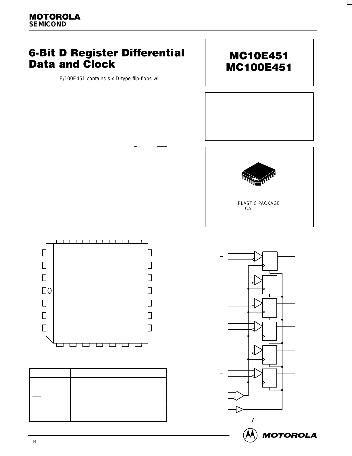
LOGIC DIAGRAM
CLK
V
BB
CLK
V
EE
MR
NC
D
0
26
27
28
2
3
4
25 24 23 22 21 20 19
18
17
16
15
14
13
12
115 6 7 8 9 10
Q
5
Q
4
V
CC
Q
3
V
CCO
Q
2
Q
1
D
0
D
0
D
0
D
1
D
1
D
2
D
2
D
3
D
3
D
4
D
4
D
5
D
5
CLK
CLK
MR
V
BB
Q
0
Q
1
Q
2
Q
3
Q
4
Q
5
D
R
D
R
D
R
D
R
D
R
D
R
1
Pinout: 28-Lead PLCC
(Top View)
* All VCC and V
CCO
pins are tied together on the die.
SEMICONDUCTOR TECHNICAL DATA
2–1
REV 2
Motorola, Inc. 1996
12/93
The MC10E/100E451 contains six D-type flip-flops with single-ended
outputs and differential data inputs. The common clock input is also
differential. The registers are triggered by a positive transition of the
positive clock (CLK) input.
A HIGH on the Master Reset (MR) input resets all Q outputs to LOW.
The VBB output is intended for use as a reference voltage for
single-ended reception of ECL signals to that device only . When using for
this purpose, it is recommended that VBB is decoupled to VCC via a
0.01µF capacitor.
The differential input structures are clamped so that the inputs of
unused registers can be left open without upsetting the bias network of
the device. The clamping action will assert the D
and the CLK sides of the
inputs. Because of the edge triggered flip-flop nature of the device
simultaneously opening both the clock and data inputs will result in an
output which reaches an unidentified but valid state. Note that the input
clamps only operate when both inputs fall to 2.5V below VCC.
• Differential Inputs: Data and Clock
• V
BB
Output
• 1100MHz Min. Toggle Frequency
• Asynchronous Master Reset
• Extended 100E V
EE
Range of – 4.2V to – 5.46V
• 75kΩ Input Pulldown Resistors
PIN NAMES
Pin Function
D0– D
5
+Data Input
D
0
– D
5
– Data Input
CLK +Clock Input
CLK – Clock Input
MR Master Reset Input
V
BB
VBB Output
Q0– Q
5
Data Outputs
6-BIT D REGISTER
DIFFERENTIAL
DATA AND CLOCK
FN SUFFIX
PLASTIC PACKAGE
CASE 776-02
Page 2
MC10E451 MC100E451
MOTOROLA ECLinPS and ECLinPS Lite
DL140 — Rev 4
2–2
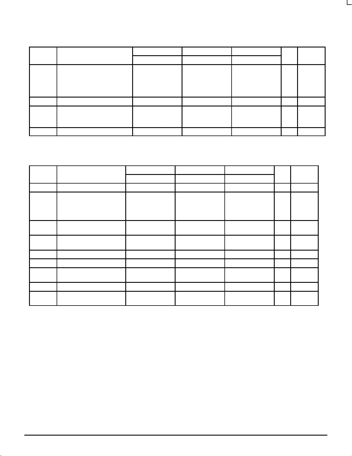
DC CHARACTERISTICS (VEE = VEE(min) to VEE(max); VCC = V
CCO
= GND)
0°C 25°C 85°C
Symbol Characteristic min typ max min typ max min typ max Unit Condition
V
BB
Output Reference Voltage V
10E –1.3
8
–1.27–1.3
5
–1.25–1.3
1
–1.1
9
100E –1.3
8
–1.26–1.3
8
–1.26–1.3
8
–1.2
6
I
IH
Input HIGH Current 150 150 150 µA
I
EE
Power Supply Current mA
10E 84 101 84 101 84 101
100E 84 101 84 101 97 116
V
CMR
Common Mode Range – 2.0 – 0.4 – 2.0 – 0.4 – 2.0 – 0.4 V 2
1. V
CMR
is referenced to the most positive side of the differential input signal. Normal operation is obtained when the “HIGH” input is within the
V
CMR
range and the input swing is greater than VPP
MIN
and < 1.0V.
AC CHARACTERISTICS (VEE = VEE(min) to VEE(max); VCC = V
CCO
= GND)
0°C 25°C 85°C
Symbol Characteristic min typ max min typ max min typ max Unit Condition
f
MAX
Max, Toggle Frequency 1100 1400 1100 1400 1100 1400 MHz
t
PLH
Propagation Delay to Output ps
t
PHL
CLK (Diff) 475 650 800 475 650 800 475 650 800
CLK (SE) 425 650 850 425 650 850 425 650 850
MR 425 600 850 425 600 850 425 600 850
t
s
Setup Time ps
D 150 –100 150 –100 150 –100
t
h
Hold Time ps
D 250 100 250 100 250 100
VPP(AC) Minimum Input Swing 150 150 159 mV 1
t
RR
Reset Recovery Time 750 600 750 600 750 600 ps
t
PW
Minimum Pulse Width ps
CLK, MR 400 400 400
t
SKEW
Within-Device Skew 100 100 100 ps 2
t
r
Rise/Fall Times ps
t
f
20 - 80% 275 450 800 275 450 800 275 450 800
1. Minimum input voltage for which AC parameters are guaranteed.
2. Within-device skew is defined as identical transitions on similar paths through a device.
Page 3

MC10E451 MC100E451
2–3 MOTOROLAECLinPS and ECLinPS Lite
DL140 — Rev 4
OUTLINE DIMENSIONS
FN SUFFIX
PLASTIC PLCC PACKAGE
CASE 776–02
ISSUE D
0.007 (0.180) T L
–M
SNSM
0.007 (0.180) T L
–M
SNSM
0.007 (0.180) T L
–M
SNSM
0.010 (0.250) T L
–M
SNSS
0.007 (0.180) T L
–M
SNSM
0.010 (0.250) T L
–M
SNSS
0.007 (0.180) T L
–M
SNSM
0.007 (0.180) T L
–M
SNSM
0.004 (0.100)
SEATING
PLANE
-T-
12.32
12.32
4.20
2.29
0.33
0.66
0.51
0.64
11.43
11.43
1.07
1.07
1.07
—
2
°
10.42
1.02
12.57
12.57
4.57
2.79
0.48
0.81
—
—
11.58
11.58
1.21
1.21
1.42
0.50
10
°
10.92
—
1.27 BSC
A
B
C
E
F
G
H
J
K
R
U
V
W
X
Y
Z
G1
K1
MIN MINMAX MAX
INCHES MILLIMETERS
DIM
NOTES:
1. DATUMS -L-, -M-, AND -N- DETERMINED
WHERE TOP OF LEAD SHOULDER EXITS
PLASTIC BODY AT MOLD PARTING LINE.
2. DIM G1, TRUE POSITION TO BE MEASURED
AT DATUM -T-, SEATING PLANE.
3. DIM R AND U DO NOT INCLUDE MOLD FLASH.
ALLOWABLE MOLD FLASH IS 0.010 (0.250)
PER SIDE.
4. DIMENSIONING AND TOLERANCING PER ANSI
Y14.5M, 1982.
5. CONTROLLING DIMENSION: INCH.
6. THE PACKAGE TOP MAY BE SMALLER THAN
THE PACKAGE BOTTOM BY UP TO 0.012
(0.300). DIMENSIONS R AND U ARE
DETERMINED AT THE OUTERMOST
EXTREMES OF THE PLASTIC BODY
EXCLUSIVE OF MOLD FLASH, TIE BAR
BURRS, GATE BURRS AND INTERLEAD
FLASH, BUT INCLUDING ANY MISMATCH
BETWEEN THE TOP AND BOTTOM OF THE
PLASTIC BODY.
7. DIMENSION H DOES NOT INCLUDE DAMBAR
PROTRUSION OR INTRUSION. THE DAMBAR
PROTRUSION(S) SHALL NOT CAUSE THE H
DIMENSION TO BE GREATER THAN 0.037
(0.940). THE DAMBAR INTRUSION(S) SHALL
NOT CAUSE THE H DIMENSION TO BE
SMALLER THAN 0.025 (0.635).
VIEW S
B
U
Z
G1
X
VIEW D-D
H
K
F
VIEW S
G
C
Z
A
R
E
J
0.485
0.485
0.165
0.090
0.013
0.026
0.020
0.025
0.450
0.450
0.042
0.042
0.042
—
2
°
0.410
0.040
0.495
0.495
0.180
0.110
0.019
0.032
—
—
0.456
0.456
0.048
0.048
0.056
0.020
10
°
0.430
—
0.050 BSC
-N-
Y BRK
D
D
W
-M-
-L-
28 1
V
G1
K1
Page 4

MC10E451 MC100E451
MOTOROLA ECLinPS and ECLinPS Lite
DL140 — Rev 4
2–4
Motorola reserves the right to make changes without further notice to any products herein. Motorola makes no warranty , representation or guarantee regarding
the suitability of its products for any particular purpose, nor does Motorola assume any liability arising out of the application or use of any product or circuit, and
specifically disclaims any and all liability , including without limitation consequential or incidental damages. “Typical” parameters which may be provided in Motorola
data sheets and/or specifications can and do vary in different applications and actual performance may vary over time. All operating parameters, including “Typicals”
must be validated for each customer application by customer’s technical experts. Motorola does not convey any license under its patent rights nor the rights of
others. Motorola products are not designed, intended, or authorized for use as components in systems intended for surgical implant into the body, or other
applications intended to support or sustain life, or for any other application in which the failure of the Motorola product could create a situation where personal injury
or death may occur. Should Buyer purchase or use Motorola products for any such unintended or unauthorized application, Buyer shall indemnify and hold Motorola
and its officers, employees, subsidiaries, affiliates, and distributors harmless against all claims, costs, damages, and expenses, and reasonable attorney fees
arising out of, directly or indirectly, any claim of personal injury or death associated with such unintended or unauthorized use, even if such claim alleges that
Motorola was negligent regarding the design or manufacture of the part. Motorola and are registered trademarks of Motorola, Inc. Motorola, Inc. is an Equal
Opportunity/Affirmative Action Employer.
How to reach us:
USA/EUROPE/Locations Not Listed: Motorola Literature Distribution; JAPAN: Nippon Motorola Ltd.; Tatsumi–SPD–JLDC, 6F Seibu–Butsuryu–Center,
P.O. Box 20912; Phoenix, Arizona 85036. 1–800–441–2447 or 602–303–5454 3–14–2 Tatsumi Koto–Ku, Tokyo 135, Japan. 03–81–3521–8315
MFAX: RMFAX0@email.sps.mot.com – TOUCHTONE 602–244–6609 ASIA/PACIFIC: Motorola Semiconductors H.K. Ltd.; 8B Tai Ping Industrial Park,
INTERNET: http://Design–NET.com 51 Ting Kok Road, Tai Po, N.T., Hong Kong. 852–26629298
MC10E451/D
*MC10E451/D*
◊
 Loading...