

Page 1
SEMICONDUCTOR TECHNICAL DATA
2–1
REV 2
Motorola, Inc. 1996
12/93
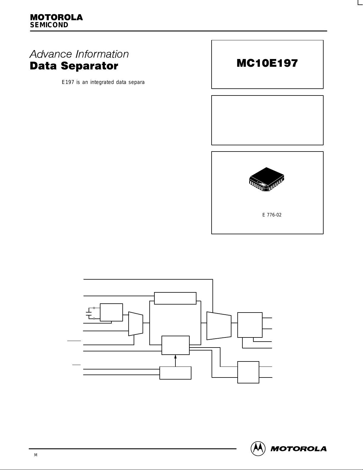
The MC10E197 is an integrated data separator designed for use in
high speed hard disk drive applications. With data rate capabilities of up
to 50Mb/s the device is ideally suited for today’s and future
state-of-the-art hard disk designs.
The E197 is typically driven by a pulse detector which reads the
magnetic information from the storage disk and changes it into ECL
pulses. The device is capable of operating on both 2:7 and 1:7 RLL
coding schemes. Note that the E197 does not do any decoding but rather
prepares the disk data for decoding by another device.
For applications with higher data rate needs, such as tape drive
systems, the device accepts an external VCO. The frequency capability
of the integrated VCO is the factor which limits the device to 50Mb/s.
A special anti-equivocation circuit has been employed to ensure timely
lock-up when the arriving data and VCO edges are coincident.
Unlike the majority of the devices in the ECLinPS family, the E197 is
available in only 10H compatible ECL. The device is available in the
standard 28-lead PLCC.
Since the E197 contains both analog and digital circuitry, separate
supply and ground pins have been provided to minimize noise coupling
inside the device. The device can operate on either standard negative
ECL supplies or, as is more common, on positive voltage supplies.
• 2:7 and 1:7 RLL Format Compatible
• Fully Integrated VCO for 50Mb/s Operation
• External VCO Input for Higher Operating Frequency
• Anti-equivocation Circuitry to Ensure PLL Lock
INTERNAL
VCO
DATA
PHASE
DETECTOR
ACQUISITION
CIRCUITRY
CHARGE
PUMP
CURRENT-
SOURCES
PHASE
DETECTOR
MUX
PHASE FREQUENCY
DETECTOR
LOGIC DIAGRAM
RDEN
REFCLK
VCOIN
EXTVCO
ENVCO
RAWD
ACQ
TYPE
CAP1
CAP2
PUMPUP
PUMPDN
RSETUP
RSETDN
RDATA
RDCLK
VCO
MUX
CLOCK &
DATA
BUFFER
This document contains information on a new product. Specifications and information herein are subject to
change without notice.
DATA SEPARATOR
FN SUFFIX
PLASTIC PACKAGE
CASE 776-02
Page 2
MC10E197
MOTOROLA ECLinPS and ECLinPS Lite
DL140 — Rev 4
2–2
CAP1
CAP2
VCOIN
V
RSETUP
PUMPDN
RAWD
RAWD
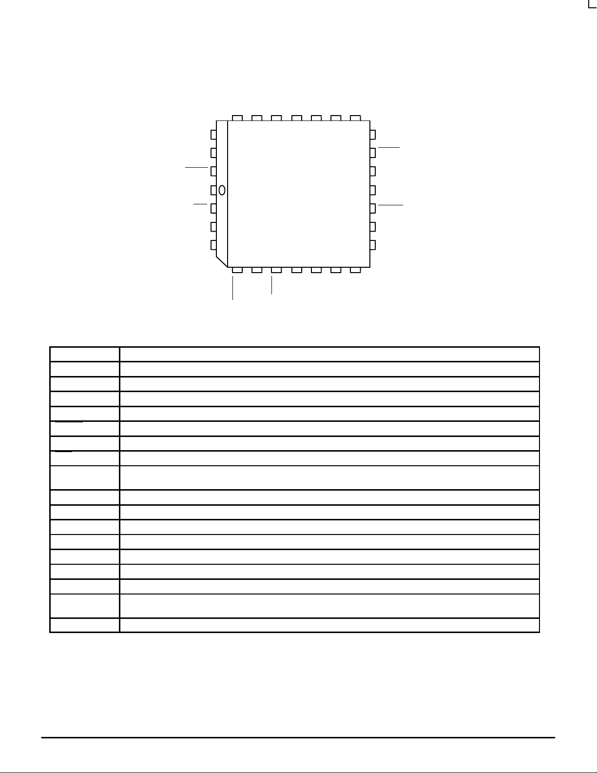
Pinout: 28-Lead PLCC (Top View)
25 24 23 22 21 20 19
18
17
16
15
14
13
12
5 6 7 8 9 10 11
26
27
28
2
3
4
RDCLK
RDCLK
V
CC
RSDATA
RSDATA
PUMPUP
RSETDN
TEST
EXTVCO
ENVCO
V
EE
ACQ
TYPE
RDEN
NC
RFFCLK
RFFCLK
CCO1
V
CCO0
V
CCVCO
V
CCVCO
1
PIN DESCRIPTIONS
REFCLK Reference clock equivalent to one clock cycle per decoding window.
RDEN Enable data synchronizer when HIGH. When LOW enable the phase/frequency detector steered by REFCLK.
RAWD Data Input to Synchronizer logic.
VCOIN VCO control voltage input
CAP1/CAP2 VCO frequency controlling capacitor inputs
ENVCO VCO select pin. LOW selects the internal VCO and HIGH selects the external VCO input. Pin floats LOW when left open.
EXTVCO External VCO pin selected when ENVCO is HIGH
ACQ Acquisition circuitry select pin. This pin must be driven HIGH at the end of the data sync field for some sync field types.
TYPE Selects between the two types of commonly used sync fields. When LOW it selects a sync field interspersed with 3 zeroes
(2:7 RLL code). When HIGH it selects a sync field interspersed with 2 zeroes (1:7 RLL code).
TEST Input included to initialize the clock flip-flop for test purposes only. Pin should be left open (LOW) in actual application.
PUMPUP Open collector charge pump output for the signal pump
PUMPDN Open collector charge pump output for the reference pump
RSETUP Current setting resistor for the signal pump
RSETDN Current setting resistor for the reference pump
RDATA Synchronized data output
RDCLK Synchronized clock output
VCC, V
CCO
,
V
CCVCO
Most positive supply rails. Digital and analog supplies are independent on chip
VEE, V
EEVCO
Most negative supply rails. Digital and analog supplies are independent on chip
Page 3

MC10E197
2–3 MOTOROLAECLinPS and ECLinPS Lite
DL140 — Rev 4
DC CHARACTERISTICS (VEE = VEE(min) to VEE(max); VCC = GND or VCC = 4.75V to 5.25V; VEE = GND)
0°C 25°C 85°C
Symbol Characteristic min typ max min typ max min typ max Unit Condition
I
IH
Input HIGH Current 150 150 150 µA 1
I
IL
Input LOW Current 0.5 0.5 0.5 µA 1
I
EE
Power Supply Current 90 150 180 90 150 180 90 150 180 mA
I
SET
Charge Pump Bias Current 0.5 5 0.5 5 0.5 5 mA 2
I
OUT
Charge Pump Output 1 1 1 µA 3
Leakage Current
V
ACT
PUMPUP/PUMPDN VCC– 2.5 V
CCVCC
– 2.5 V
CCVCC
– 2.5 V
CC
V
Active Voltage Range
10H LOGIC LEVELS
DC CHARACTERISTICS (VEE = VEE(min) to VEE(max); VCC = V
CCO
+ V
CCO1
= V
CCVCO
= GND)
0°C 25°C 85°C
Symbol Characteristic min typ max min typ max min typ max Unit Condition
V
OH
Output HIGH Voltage –1020 – 840 – 980 – 810 – 910 –720 mV
V
OL
Output LOW Voltage –1950 –1630 –1950 –1630 –1950 –1595 mV
V
IH
Input HIGH Voltage –1170 –840 –1130 – 810 –1060 –720 mV
V
IL
Input LOW Voltage –1950 –1480 –1950 –1480 –1950 –1445 mV
POSITIVE EMITTER COUPLED LOGIC LEVELS
DC CHARACTERISTICS (VEE = V
EEVCO
= GND; VCC = V
CCO1
= V
CCVCO
= +5 volts*)
0°C 25°C 85°C
Symbol Characteristic min typ max min typ max min typ max Unit Condition
V
OH
Output HIGH Voltage 3980 4160 4020 4190 4090 4280 mV
V
OL
Output LOW Voltage 3050 3370 3050 3370 3050 3405 mV
V
IH
Input HIGH Voltage 3830 4160 3870 4190 3940 4280 mV
V
IL
Input LOW Voltage 3050 3520 3050 3050 3050 3555 mV
1. *VOH and VOL levels will vary 1:1 with V
CC
AC CHARACTERISTICS (VEE = VEE(min) to VEE(max); VCC = GND or VCC = 4.75V to 5.25V; VEE = GND)
0°C 25°C 85°C
Symbol Characteristic min max min max min max Unit Condition
t
s
Time from RDATA Valid to
Rising Edge of RDCLK
T
VCO
– 550 T
VCO
– 500 T
VCO
– 500 ps 4,7
t
H
Time from Rising Edge of
RDCLK to RDATA invalid
T
VCO
T
VCO
T
VCO
ps 4,7
t
SKEW
Skew Between RDATA and
RDATA
300 300 300 ps
f
VCO
Frequency of the VCO 150 150 150 MHz 5
Tuning Ratio 1.53 1.87 1.53 1.87 1.53 1.87 6
1. Applies to the input current for each input except VCOIN
2. For a nominal set current of 3.72mA, the resistor values for RSETUP and RSETDN should be 130Ω(0.1%). Assuming no variation between
these two resistors, the current match between the PUMPUP and PUMPDN output signals should be within ±3%. I
SET
is calculated as (VEE+
1.3v – VBE)/R; where R is RSETUP or RSETDN and a nominal value for VBE is 0.85 volts.
3. Output leakage current of the PUMPUP or PUMPDN output signals when at a LOW level.
4. T
VCO
is the period of the VCO.
5. The VCO frequency determined with VCOIN = VEE + 0.5 volts and using a 10pF tuning capacitor.
6. The tuning ratio is defined as the ratio of f
VCOMAX
to F
VCOMIN
where f
VCOMAX
is measured at VCOIN = 1.3V + VEE and f
VCOMAX
is measured
at VCOIN = 2.6V + VEE.
Page 4
MC10E197
MOTOROLA ECLinPS and ECLinPS Lite
DL140 — Rev 4
2–4
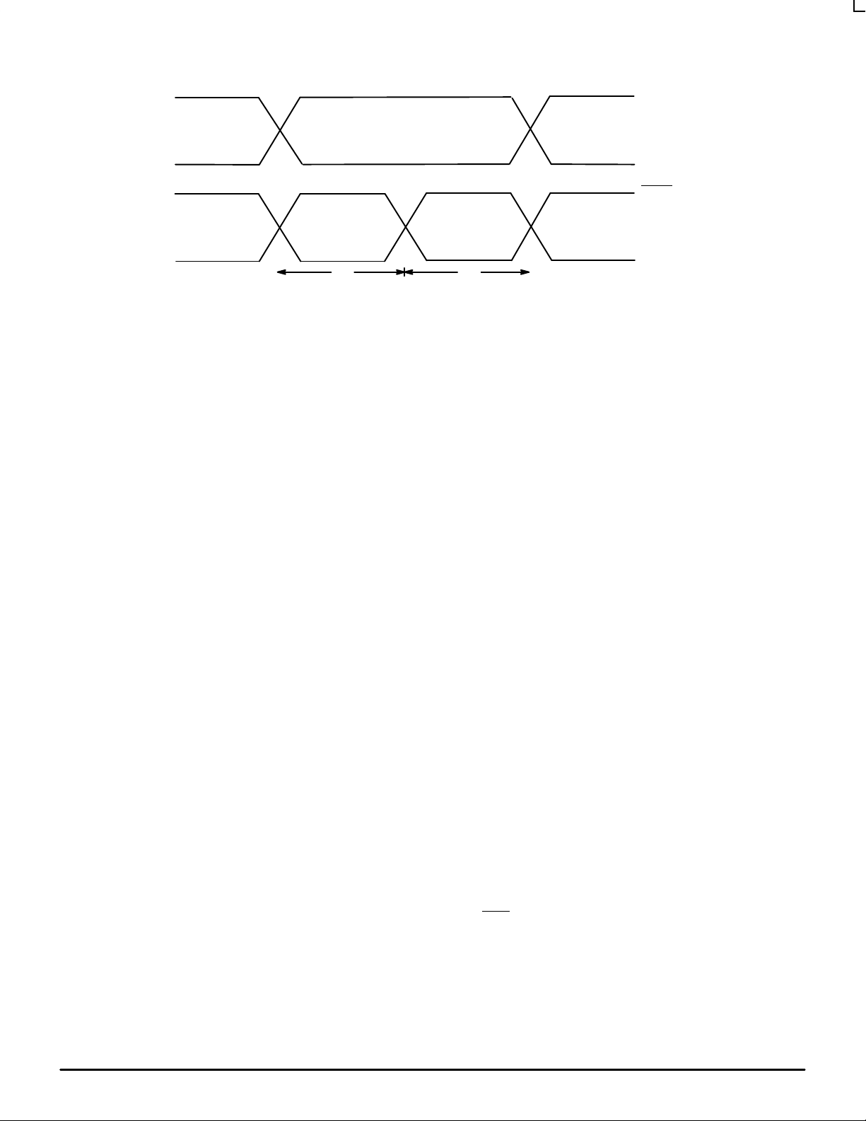
RDATA
RDATA
RDCLK
RDCLK
t
S
t
H
SETUP AND HOLD TIMING DIAGRAMS
APPLICATIONS INFORMATION
General Operation
Operation
The E197 is a phase-locked loop circuit consisting of an
internal VCO, a Data Phase detector with associated
acquisition circuitry, and a Phase/Frequency detector (Figure
1). In addition, an enable pin(ENVCO) is provided to disable
the internal VCO and enable the external VCO input. Hence,
the user has the option of supplying the VCO signal.
The E197 contains two phase detectors: a data phase
detector for synchronizing to the non-periodic pulses in the
read data stream during the data read mode of operation, and
a phase/ frequency detector for frequency (and phase) locking
to an external reference clock during the “idle” mode of
operation. The read enable (RDEN) pin muxes between these
two detectors.
Data Read Mode
The data pins (RAWD) are enabled when the RDEN pin is
placed at a logic high level, thus enabling the Data Phase
detector (Figure1) and initiating the data read mode. In this
mode, the loop is servoed by the timing information taken from
the positive edges of the input data pulses. This phase
detector samples positive edges from the RAWD signal and
generates both a pump up and pump down pulse from any
edge of the input data pulse. The leading edge of the pump up
pulse is time modulated by the leading edge of the data signal,
whereas the rising edge of the pump up pulse is generated
synchronous to the VCO clock. The falling edge of the pump
down pulse is synchronous to the falling edge of the VCO
clock and the rising edge of the pump down signal is
synchronous to the rising edge of the VCO clock. Since both
edges of the VCO are used the internal clock a duty cycle of
50%. This pulse width modulation technique is used to
generate the servoing signal which drives the VCO. The pump
down signal is a reference pulse which is included to provide
an evenly balanced differential system, thereby allowing the
synthesis of a VCO input control signal after appropriate signal
processing by the loop filter.
By using suitable external filter circuitry, a control signal for
input into the VCO can be generated by inverting the pump
down signal, summing the inverted signal with the pump up
signal and averaging the result. The polarity of this control
signal is defined as zero when the data edges lead the clock
by a half clock cycle. If the data edges are advanced with
respect to the zero polarity data/VCO edge relationship, the
control signal is defined to have a negative polarity; whereas
if the VCO is advanced with respect to the zero polarity
data/VCO edge relationship, the control signal is defined to
have a positive polarity . If there is no data edge present at the
RAWD input, the corresponding pump up and pump down
outputs are not generated and the resulting control output is
zero.
Acquisition Circuitry
The acquisition circuitry is provided to assist the data phase
detector in phase locking to the sync field that precedes the
data. For the case in which lock-up is attempted when the data
edges are coincident with the VCO edges, the pump down
signal may enter an indeterminate state for an unacceptably
long period due to the violation of internal set up and hold
times. After an initial pump down pulse, the circuit blocks
successive pump down pulses, and inserts extra pump up
pulses, during portions of the sync field that are known to
contain zeros. Thus, the data phase detector is forced to have
a nonzero output during the lock-up period, and the restoring
force ensures correction of the loop within an acceptable time.
Hence, this circuitry provides a quasi-deterministic pump
down output signal, under the condition of coincident data and
VCO edges, allowing lock-up to occur with excessive delays.
The ACQ
line is provided to disable (disable = HIGH) the
acquisition circuit during the data portion of a sector block.
Typically, this circuit is enabled at the beginning of the sync
field by a one-shot timer to ensure a timely lock-up.
The TYPE line allows the choice between two sync field
preamble types; transitions interspersed with two zeros
between transitions. These types of sync fields are used with
the 1:7 and 2:7 coding schemes, respectively.
Page 5
MC10E197
2–5 MOTOROLAECLinPS and ECLinPS Lite
DL140 — Rev 4
Idle Mode
In the absence of data or when the drive is writing to the disk,
PLL servoing is accomplished by pulling the read enable line
(RDEN) low and providing a reference clock via the REFCLK
pins. The condition whereby RDEN is low selects the
Phase/Frequency detector (Figure 1) and the 10E197 is said
to be operating in the “idle mode”. In order to function as a
frequency detector the input waveform must be periodic. The
pump up and pump down pulses from the Phase/Frequency
detector will have the same frequency , phase and pulse width
only when the two clocks that are being compared have their
positive edges aligned and are of the same frequency.
As with the data phase detector, by using suitable external
filter circuitry, a VCO input control signal can be generated by
inverting the pump down signal, summing the inverted signal
with the pump up signal and averaging the result. The polarity
of this control signal is defined as zero when all positive edges
of both clocks are coincident. For the case in which the
frequencies of the two clocks are the same but the clock edges
of the reference clock are slightly advanced with respect to the
VCO clock, the control clock is defined to have a positive
polarity. A control signal with negative polarity occurs when
the edges of the reference clock are delayed with respect to
those of the VCO. If the frequencies of the two clocks are
different, the clock with the most edges per unit time will initiate
the most pulses and the polarity of the detector will reflect the
frequency error. Thus, when the reference clock is high in
frequency than the VCO clock the polarity of the control signal
is positive; whereas a control signal with negative polarity
occurs when the frequency of the reference clock is lower than
the VCO clock.
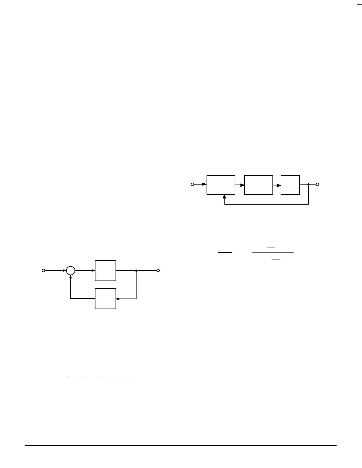
Phase-Lock Loop Theory
Introduction
Phase lock loop (PLL) circuits are fundamentally feedback
systems used to synchronize the frequency of an oscillator to
an incoming signal. In addition to frequency synchronization,
the PLL circuitry is designed to minimize the phase difference
between the system input and output signals. A block diagram
of a feedback control system is shown in Figure 1.
where:
A(s) is the product of the feed-forward transfer functions.
Figure 1. Feedback System
Xi(s) Xo(s)
A(s)
β
(s)
+
–
Xe(s)
R
β(s) is the product of the feedback transfer functions.
The transfer function for this closed loop system is
Xo(s)
Xi(s)
=
A(s)
1 + A(s)β(s)
Typically, phase lock loops are modeled as feedback
systems connected in a unity feedback configuration (β(s)=1)
with a phase detector, a VCO (voltage controlled oscillator),
and a loop filter in the feed-forward path, A(s). Figure 2
illustrates a phase lock loop as a feedback control system in
block diagram form.
F
i
F
o
PHASE
DETECTOR
K
f
V
CO
K
o
s
Figure 2. Phase Lock Loop Block Diagram
The closed loop transfer function is:
Xo(s)
Xi(s)
=
K
φ
K
o
s
F(s)
K
o
s
1 + K
φ
F(s)
where:
Kφ= the phase detector gain.
Ko= the VCO gain. Since the VCO introduces a
pole at the origin of the s-plane, Ko is divided
by s.
F(s) = the transfer function of the loop filter.
The 10E197 is designed to implement the phase detector
and VCO functions in a unity feedback loop, while allowing the
user to select the desired filter function.
Gain Constants
As mentioned, each of the three sections in the phase lock
loop block diagram has an associated open loop gain
constant. Further, the gain constant of the filter circuitry is
composed of the product of three gain constants, one for each
filter subsection. The open loop gain constant of the
feed-forward path is given by
Kol = Kφ * Ko * K1 * Kl * K
d
eqt. 1
and obtained by performing a root locus analysis.
Phase Detector Gain Constant
The gain of the phase detector is a function of the operating
mode and the data pattern. The 10E197 provides data
LOOP FILTER
F(s)
Page 6

MC10E197
MOTOROLA ECLinPS and ECLinPS Lite
DL140 — Rev 4
2–6
separation for signals encoded in 2:7 or 1:7 RLL encoding
schemes; hence, Tables 1 and 2 are coding tables for these
schemes. Table 3 lists nominal phase detector gains for both
2:7 and 1:7 sync fields.
NRZ Data Sequence Code Sequence
00 1000
01 0100
100 001000
101 100100
111 000100
1100 00001000
1101 00100100
Table 1. 2:7 RLL Encoding Table
NRZ Data Sequence Code Sequence
00 X01
01 010
10 X00
1100 010001
1101 X00000
1110 X00001
1111 010000
An X in the leading bit of a code sequence is assigned the
complement of the bit
Table 2. 1:7 RLL Encoding Table
Sync Pattern Read Mode Idle Mode
2:7 121 mV/radian 484 mV/radian
1:7 161 mV/radian 483 mV/radian
Table 3. Phase Detector Gain Constants
VCO Gain Constant
The gain of the VCO is a function of the tuning capacitor.
For a value of 10pF a nominal value of the gain, Ko, is
20MHz per volt.
Filter Circuitry Gain Constant(s)
The open loop gain constant of the filter circuitry is given by:
Kfc = K1 * Kl * K
d
eqt. 2
The individual gain constants are defined in the appropriate
subsections of this document.
Loop Filter
The two major functions of the loop filter are to remove any
noise or high frequency components present in the phase
detector output signal and, more importantly, to control the
characteristics which determine the dynamic response of the
phase lock loop; i.e. capture range, loop bandwidth, capture
time, and transient response.
Although a variety of loop filter configurations exist, this
section will only describe a filter capable of performing the
signal processing as described in the Data Read Mode and
the Idle Mode sections. The loop filter consists of a differential
summing amplifier cascaded with an augmenting integrator
which drives the VCOIN input to the 10E197 through a resistor
divider network (Figure 3).
The transfer function and the element values for the loop
filter are derived by dividing the filter into three cascaded
subsections: filter input, augmenting integrator, and the
voltage divider network (Figure 4).
Loop Filter Transfer Function
The open loop transfer function of the phase lock loop is the
product of each individual filter subsection, as well as the
phase detector and VCO. Thus, the open loop filter transfer
function is:
Fo(s) = Kφ *
Fd(s) = Kd *
* F1(s) * Fl(s) * Fd(s)
K
o
s
F1(s) = K1 *
1
(s + p1)
*
1
[s2 + (2ζω ) s + ω2 ]
[s2 + (2ζω ) s + ω2 ]
where:
Fl(s) = Kl *
1
s
*
(s + z)
1
(s + p2)
o2o2
o1 o1
Figure 3. Loop Filter Circuitry
PUMPUP
PUMPDN
V
EEVCO
V
EEVCO
V
CCVCO
V
CCVCO
V
EEVCO
V
EEVCO
R
1
R
1
R
IA
R
A
C
A
R
V
R
O
D
B
C
O
R
3
R
1
R
1
C
IN
C
IN
V
O
MC34182
MC34182
Page 7

MC10E197
2–7 MOTOROLAECLinPS and ECLinPS Lite
DL140 — Rev 4
VOLTAGE
DIVIDER
FO(s)
AUGMENTNG
INTEGRATOR
FI(s)
FILTER
INPUT
F1(s)
Fi(s)
F
(s)=F1
(s)Fi(s)Fd(s)
Figure 4. Loop Filter Block Diagram
A root locus analysis is performed on the open loop transfer
function to determine the final pole-zero locations and the
open loop gain constant for the phase lock loop. Note that the
open loop gain constant impacts the crossover frequency and
that a lower frequency crossover point means a much more
efficient filter. Once these positions and constants are
determined the component values may be calculated.
I
PUMPUP
I
PUMPDN
V
EEVCOVEEVCO
V
EEVCO
V
EEVCO
V
CCVCO
R
1
R
1
R
1
R
1
C
IN
V
01
MC34182
Figure 5. Filter Input Sunsection
Filter Input
The primary function of the filter input subsection is to
convert the output of the phase detector into a single ended
signal for subsequent processing by the integrator circuitry.
This subsection consists of the 10E197 charge pump current
sinks, two shunt capacitors, and a differential summing
amplifier (Figure 5).
Hence, this portion of the filter circuit contributes a real pole
and two complex poles to the overall loop transfer function
F(s). Before these pole locations are selected, appropriate
values for the current setting resistors (RSETUP and
RSETDN) must be ascertained. The goal in choosing these
resistor values is to maximize the gain of the filter input
subsection while ensuring the charge pump output transistors
operate in the active mode. The filter input gain is maximized
for a charge pump current of 1.1mA; a value of 464Ω for both
RSETUP and RSETDN yields a nominal charge pump current
of 1.1mA.
It should be noted that a dual bandwidth implementation
of the phase lock loop may be achieved by modifying the
current setting resistors such that an electronic switch
enables one of two resistor configurations. Figure 6 shows
a circuit configuration capable of providing this dual
bandwidth function. Analysis of the filter input circuitry yields
the transfer function:
F1(s) = K1 *
1
(s + p1)
*
1
where:
The gain constant is defined as:
K1 = A1 *
1
C
IN
eqt. 3
A1= op-amp gain constant for the
selected pole positions.
CIN = phase detector shunt capacitor.
[s2 + (2ζω ) s + ω2 ]
o1 o1
The real pole is a function of the input resistance to the
op-amp and the shunt capacitors connected to the phase
detector output. For stability the real pole must be placed
beyond the unity gain frequency; hence, this pole is typically
placed midway between the unity crossover and phase
detector sampling frequency, which should be about ten
times greater.
ELECTRONIC SWITCH
V
EEVCO
V
EEVCO
RSETUP
RSETDN
464
Ω
464
Ω
464
Ω
464
Ω
Figure 6. Dual Bandwidth Current
Source Implementation
The second order pole set arises from the two pole model
for an op-amp. The open loop gain and the first open loop pole
for the op-amp are obtained from the data sheets. Typically,
op-amp manufacturers do not provide information on the
location of the second open loop pole; however, it can be
approximated by measuring the roll off of the op-amp in the
open loop configuration. The second pole is located where the
gain begins to decrease at a rate of 40dB per decade. The
inclusion of both poles in the differential summing amplifier
transfer function becomes important when closing the
feedback path around the op-amp because the poles migrate;
and this migration must be accounted for to accurately
determine the phase lock loop transient performance.
Typically the op-amp poles can be approximated by a pole
pair occurring as a complex conjugate pair making an angle
of 45° to the real axis of the complex frequency plane. Two
constraints on the selection of the op-amp pole pair are that
Page 8

MC10E197
MOTOROLA ECLinPS and ECLinPS Lite
DL140 — Rev 4
2–8
the poles lie beyond the crossover frequency and they are
positioned for near unity gain operation. Performing a root
locus analysis on the op-amp open loop configuration and
adhering to the two constraints yields the pole positions
contributed by the op-amp.
Determination of Element Values
Since the difference amplifier is configured to operate as a
differential summer the resistor values associated with the
amplifier are of equal value. Further, the typical input
resistance to the summing amplifier is 1kΩ; thus, the op-amp
resistors are set at 1 kΩ. Having set the input resistance to the
op-amp and selected the position of the real pole, the value of
the shunt capacitors is determined using the following
relationship:
p1 =
1
2πR1C
IN
eqt. 4
Augmenting Integrator
The augmenting integrator consists of an active filter with a
lag-lead network in the feedback path (Figure 7).
V
IN
V
CCVCO
MC34182
R
IA
R
A
C
A
V
O2
R
IA
Figure 7. Integrator Subsection
Analysis of this portion of the filter circuit yields the transfer
function:
F1(s) = Kl *
1
s
*
(s + z)
[s2 + (2ζω ) s + ω2 ]
o2o2
The gain constant is defined as:
where:
Al = op-amp gain constant for selected pole positions.
RA = integrator feedback resistor.
RlA = integrator input resistor.
Kl = Al *
R
A
R
lA
eqt. 5
The integrator circuit introduces a zero, a pole at the origin,
and a second order pole set as described by the two pole
model for an op-amp. As in the case of the differential
summing amplifier, we assume the op-amp pole pair occur as
a complex conjugate pair making an angle of 45° to the real
axis of the complex frequency plane; are positioned for near
unity gain operation; and are located beyond the crossover
frequency. Since both the summing and integrating op-amps
are realized by the same type of op-amp (MC34182D), the
open loop pole positions for both amplifiers will be the same.
Further, the loop transfer function contains two poles
located at the origin, one introduced by the integrator and the
other by the VCO; hence a zero is necessary to compensate
for the phase shift produced by these poles and ensure loop
stability. The op-amp will be stable if the crossover point
occurs before the transfer function phase angle becomes
180°. The zero should be positioned much less than one
decade before the unity gain frequency.
As in the case of the filter input circuitry, the poles and zero
from this analysis will be used as open loop poles and a zero
when performing the root locus analysis for the complete
system.
Determination of Element Values
The location of the zero is used to determine the element
values for the augmenting integrator. The value of the
capacitor, CA, is selected to provide adequate charge storage
when the loop is not sampling data. A value of 0.1µF is
sufficient for most applications; this value may be increased
when the RDCLK frequency is much lower than 4 MHz. The
value of RA is governed by:
z =
1
2πRAC
A
eqt. 6
For unity gain operation of the integrating op-amp the value of
RlA is selected such that:
RlA = RA eqt. 7
It should be noted that although the zero can be tuned by
varying either RA or CA, caution must be exercised when
adjusting the zero by varying CA because the integrator gain is
also a function of CA. Further, the gain of the loop filter can be
adjusted by changing the integrator input resistor RlA.
Voltage Divider
The input range to the VCOIN input is from 1.3V + VEE to
2.6V + VEE; hence, the output from the augmenting amplifier
section must be attenuated to meet the VCOIN constraints. A
simple voltage divider network provides the necessary
attenuation (Figure 8).
V
IN
R
V
R
O
D
B
C
d
V
O
Figure 8. Voltage Divider Subsection
Page 9

MC10E197
2–9 MOTOROLAECLinPS and ECLinPS Lite
DL140 — Rev 4
In addition, a shunt filter capacitor connected between the
VCOIN input pin and VEE provides the voltage divider
subsection with a single time constant transfer function that
adds a pole to the overall loop filter. The transfer function for
the voltage divider network is:
Fd(s) = Kd *
1
(s + p2)
The gain constant, Kd, is defined as:
Kd =
1
Rv C
d
eqt. 9
The value of Kd is easily extracted by rearranging Equation 1:
Kd =
K
ol
Kφ * Ko * K1 * K
l
eqt. 10
The gain constant Kd is set such that the output from the
integrator circuit is within the range 1.3V +VEE to 2.6V +VEE.
The pole for the voltage divider network should be positioned
an octave beyond that for the filter input.
Determination of Element Values
Once the pole location and the gain constant Kd are
established the resistor values for the voltage divider network
are determined using the design guidelines mentioned above
and from the following relationship:
K
d
2π p2
=
R
o
Ro + R
v
Having determined the resistor values, the filter capacitor is
calculated by rearranging Equation 9:
Cd =
1
Rv K
d
eqt. 9a
Finally, a bias diode is included in the voltage divider network
to provide temperature compensation. The finite resistance of
this diode is neglected for these calculations.
Page 10

MC10E197
MOTOROLA ECLinPS and ECLinPS Lite
DL140 — Rev 4
2–10
Calculations For a 2:7 Coding Scheme
Introduction
The circuit component values are calculated for a 2:7 coding
scheme employing a data rate of 23Mbit/sec. Since the
number of bits is doubled when the data is encoded, the data
clock is at half the frequency of the RDCLK signal. Thus, the
operating frequency for these calculations is 46MHz. Further,
the pole and zero positions are a function of the data rate;
hence, the component values derived by these calculations
must be scaled if a different operating frequency is used.
Finally, it should be noted that the values are optimized for
settling time.
The analysis is divided into three parts: static pole
positioning, dynamic pole positioning, and dynamic zero
positioning. Dynamic poles and zeros are those which the
designer may position, to yield the desired dynamic response,
through the judicious choice of element values. Static poles
are not directly controlled by the choice of component values.
Static Poles
Each op-amp introduces a pair of “static” complex
conjugate poles which must lie beyond the crossover
frequency. As obtained from the data sheets and laboratory
measurements, the two open loop poles for the MC34182D
are:
P*1a = – 0.1Hz
P*1b = –11.2Hz
Performing a root locus analysis and following the two
guidelines previously stated, an acceptable pole set is:
P1a = – 5.65 + j5.65MHz
P1b = – 5.65 – j5.65MHz
Both op-amps introduce a set of static complex conjugate
poles at these positions for a total of four poles. Further, the
loop gain for each op-amp associated with these pole
positions is determined from the root locus analysis to be:
A1 = A2 = 2.48 e15
V
V
In addition to the op-amps, the integrator and the VCO each
contribute a static pole at the origin. Thus, there are a total of
six static poles.
Dynamic Poles
The filter input and the voltage divider sections each
contribute a dynamic pole. As stated previously , the filter input
pole should be positioned midway between the unity
crossover point and the phase detector sampling frequency.
Hence, the open loop filter input pole position is selected as:
P*1 = –1.24MHz
The voltage divider pole is set approximately one octave
higher than the filter input pole. Thus the open loop voltage
divider pole position is picked to be:
P*2 = – 2.57MHz
Dynamic Zero
Finally, the zero is positioned much less than one decade
before the crossover frequency; for this design the zero is
placed at:
z = – 311Hz
Once the dynamic pole and zero positions have been
determined, the phase margin is determined using a Bode
plot; if the phase margin is not sufficient, the dynamic poles
may be moved to improve the phase margin. Finally, a root
locus analysis is performed to obtain the optimum closed loop
pole positions for the dynamic characteristics of interest.
Component Values
Having determined the closed loop pole and zero positions
the component values are calculated. From the root locus
analysis the dynamic pole and zero positions are:
P1 = – 573kHz
P2 = – 3.06MHz
z = – 311Hz
Filter Input Subsection
Rearranging Equation 4:
CIN =
1
2π R1 p1
and substituting 573 kHz for the pole position and 1 kΩ for
the resistor value yields:
CIN = 278 pF
Augmenting Integrator Subsection
Rearranging Equation 6:
RA =
1
2
π z
C
A
and substituting 31 1Hz for the zero position and 0.1µF for the
capacitor value yields:
RA = 5.11kΩ
Page 11

MC10E197
2–11 MOTOROLAECLinPS and ECLinPS Lite
DL140 — Rev 4
From Equation 7 the value for the other resistors associated
with the integrator op-amp are set equal to RA:
RlA = RA = 5.11kΩ
Voltage Divider Subsection
The element values for the voltage divider network are
calculated using the relationships presented in Equations 8,
9, and 10 with the constraint that this divider network must
produce a voltage that lies within the range 1.3V + VEE to 2.6V
+ VEE.
Restating Equation 9,
Kd =
K
ol
Kφ * Ko * K1 * K
l
From the root locus analysis Kol is determined to be:
Kol = 1.585 e51
V
mA sec
3
From Equation 3
K1 = A1 *
1
C
IN
and the gain constant K1 is:
K1 = 8.90 e21
V
mA sec
From Equation 5
Kl = Al *
R
A
R
lA
and the gain constant Kl is:
Kl = 2.48 e15
V
V
Having determined the gain constant Kd , the value of Rv, is
selected such that the constraints Rv > Ro and:
K
d
2π p2
=
R
o
Ro + R
v
are fulfilled. The pole position P2 is determined from the root
locus analysis to be:
P2 = – 3.06MHz
Hence, Rv is selected to be:
Rv = 2.15kΩ
and Ro is calculated to be:
Ro = 700Ω
Finally, using Equation 8a:
Cd =
1
Rv K
d
eqt. 8a
the capacitor value, Cd is:
Cd = 98pF
Note that the voltage divider section can be used to set the
gain, but the designer is cautioned to be sure the input
value to VCOIN is within the correct range.
Component Scaling
As mentioned, these design equations were developed for
a data rate of 23 Mbit/sec. If the data rate is different from the
nominal design value the reactive elements must be scaled
accordingly. The following equations are provided to facilitate
scaling and were derived with the assumptions that a 2:7
coding scheme is used and that the RDCLK signal is twice the
frequency of the data clock.
CIN = 278 *
46
f
eqt. 11
(pF)
46
f
Cd = 98 * eqt. 12(pF)
where f is the RDCLK frequency in MHz.
Example for an 11 Mbit/sec Data Rate
As an example of scaling, assume the given filter and a 2:7
code are used but the data rate is 11Mbit/sec. The dynamic
pole positions, and therefore the bandwidth of the loop filter,
are a function of the data rate. Thus a slower data rate will
force the dynamic poles and the bandwidth to move to a lower
frequency. From Equation 11 the value of CIN is:
CIN = 581pF
and from Equation 12 the value of Cd is:
Cd = 205pF
Thus the element values for the filter are:
Filter Input Subsection:
CIN = 581pF
R1 = 1kΩ
Integrator Subsection:
CA = 0.1µF
RA = 5.11kΩ
RlA = 5.11kΩ
Voltage Divider Subsection:
Cd = 205pF
Rv = 2.15kΩ
Ro = 700kΩ
Page 12

MC10E197
MOTOROLA ECLinPS and ECLinPS Lite
DL140 — Rev 4
2–12
Note, the poles P1 and P2 are now located at:
P1 = – 274kHz
P2 = –1.47MHz
And, the open loop filter unity crossover point is at 300kHz.
The gain can be adjusted by changing the value of RlA and the
value of Cd. Varying the gain by changing Cd is not
recommended because this will also move the poles, hence
affect the dynamic 2 performance of the filter.
Calculations For a 1:7 Coding Scheme
Introduction
The circuit component values are calculated for a 1:7
coding scheme employing a data rate of 20Mbit/sec. Since the
number of bits increases from two to three when the data is
encoded, the data clock is at two-thirds the frequency of the
RDCLK signal. Thus, the operating frequency for these
calculations is 30MHz. As in the case of the 2:7 coding
scheme the pole and zero positions are a function of the data
rate, hence the component values derived by these
calculations must be scaled if a different operating frequency
is used.
Again, the analysis is divided into three parts: static pole
positioning, dynamic pole positioning, and dynamic zero
positioning.
Static Poles
As in the 2:7 coding example, an MC34182D op-amp is
employed, hence the pole set is:
P1a = – 5.65 + j5.65MHz
P1b = – 5.65
– j5.65MHz
and the open loop gain is:
Al = A2 = 2.48 e15
V
V
Since the op-amps introduce a set of complex conjugate
poles, a total of four poles are introduced by the op-amp. In
addition, the integrator and the VCO each contribute a pole at
the origin for a total of six static poles.
Dynamic Poles
The filter input and the voltage divider sections each
contribute a dynamic pole. As stated previously , the filter input
pole should be positioned midway between the unity
crossover point and the phase detector sampling frequency.
Hence, the open loop filter input pole position is selected as:
P
*
1
= –1.1MHz
The voltage divider pole is set approximately one octave
higher than the filter input pole. Thus, the open loop voltage
divider pole position is selected as:
P
*
2
= – 2.28MHz
Dynamic Zero
Finally, the zero is positioned much less than one decade
before the crossover frequency; for this design the zero is
placed at:
z = – 311Hz
Once the dynamic pole and zero positions have been
determined, the phase margin is determined using a Bode
plot; if the phase margin is not sufficient, the dynamic poles
may be moved to improve the phase margin. Finally, a root
locus analysis is performed to obtain the optimum closed loop
pole positions for the dynamic characteristics of interest.
Component Values
Having determined the closed loop pole and zero positions
the component values are calculated. From the root locus
analysis the dynamic pole and zero positions are:
P1 = – 541kHz
P2 = – 2.73MHz
z = – 311Hz
Filter Input Subsection
Rearranging Equation 4
CIN =
1
2π R1 p1
and substituting 541kHz for the pole position and 1.0kΩ for
the resistor value yields:
CIN = 294 pF
Augmenting Integrator Subsection
Rearranging Equation 6
RA =
1
2π z C
A
and substituting 31 1Hz for the zero position and 0.1µF for the
capacitor value yields:
RA = 5.11kΩ
From Equation 7 the value for the other resistors associated
with the integrator op-amp are set equal to RA:
RlA = RA = 5.11kΩ
Page 13

MC10E197
2–13 MOTOROLAECLinPS and ECLinPS Lite
DL140 — Rev 4
Voltage Divider Subsection
The element values for the voltage divider network are
calculated using the relationships presented in Equations 8,
9, and 10 with the constraint that this divider network must
produce a voltage that lies within the range 1.3V + VEE to 2.6V
+ VEE.
Restating Equation 9,
Kd =
K
ol
Kφ * Ko * K1 * K
l
From the root locus analysis Kol is determined to be:
Kol = 1.258 e51
V
MA
SEC
3
From Equation 3:
K1 = A1 *
1
C
IN
and the gain constant K1:
K1 = 8.42 e21
V
mA sec
From Equation 5:
Kl = Al *
R
A
R
lA
and the gain constant Kl is:
Kl = 2.48 e15
V
V
Kd = 2.98 e6 sec
–1
Having determined the gain constant Kd , the value of Rv, is
selected such that the constraints Rv > Ro and:
K
d
2πp2
=
R
o
Ro + R
v
are fulfilled. The pole position P2 is determined from the root
locus analysis to be:
P2 = – 2.73MHz
Hence, Rv is selected to be:
Rv = 2.15kΩ
and Ro is calculated to be:
Ro = 453Ω
Finally, using Equation 8a:
Cd =
1
Rv K
d
eqt. 8a
the capacitor value, Cd is calculated to be:
Cd = 156pF
Again, note the voltage divider section can be used to set the
gain, but the designer is cautioned to be sure the input value to
VCOIN is within the correct range.
Component Scaling
As mentioned, these design equations were developed for
a data rate of 20Mbit/sec. If the data rate is different from the
nominal design value the reactive elements must be scaled
accordingly. The following equations provided are to facilitate
scaling and were derived with the assumptions that a 1:7
coding scheme is used and that the RDCLK signal is twice the
frequency of the data clock:
CIN = 294 *
30
f
eqt. 13(pF)
30
f
Cd = 156 * eqt. 14(pF)
where f is the RDCLK frequency in MHz.
Example for an 10 Mbit/sec Data Rate
As an example of scaling, assume the given filter and a 1:7
code are used but the data rate is 10Mbit/sec. The dynamic
pole positions and, therefore, the bandwidth of the loop filter,
are a function of the data rate. Thus, a slower data rate will
force the dynamic poles and the bandwidth to move to a lower
frequency. From Equation 13 the value of CIN is:
CIN = 588pF
and from Equation 14 the value of Cd is:
Cd = 312pF
Thus, the element values for the filter are:
Filter Input Subsection:
CIN = 588pF
R1 = 1.0kΩ
Integrator Subsection:
CA = 0.1µF
RA = 5.11kΩ
RlA = 5.11kΩ
Page 14

MC10E197
MOTOROLA ECLinPS and ECLinPS Lite
DL140 — Rev 4
2–14
Voltage Divider Subsection:
Cd = 312pF
Rv = 2.15kΩ
Ro = 453kΩ
Note, the poles P1 and P2 are now located at:
P1 = – 271kHz
P2 = –1.36MHz
And, the open loop filter unity crossover point is at 300kHz.
As in the case of the 2:7 coding scheme, the gain can be
adjusted by changing the value of RlA and the value of Cd.
Varying the gain by changing Cd is not recommended
because this will also move the poles, hence affect the
dynamic performance of the filter.
Page 15

MC10E197
2–15 MOTOROLAECLinPS and ECLinPS Lite
DL140 — Rev 4
OUTLINE DIMENSIONS
FN SUFFIX
PLASTIC PLCC PACKAGE
CASE 776–02
ISSUE D
0.007 (0.180) T L
–M
SNSM
0.007 (0.180) T L
–M
SNSM
0.007 (0.180) T L
–M
SNSM
0.010 (0.250) T L
–M
SNSS
0.007 (0.180) T L
–M
SNSM
0.010 (0.250) T L
–M
SNSS
0.007 (0.180) T L
–M
SNSM
0.007 (0.180) T L
–M
SNSM
0.004 (0.100)
SEATING
PLANE
-T-
12.32
12.32
4.20
2.29
0.33
0.66
0.51
0.64
11.43
11.43
1.07
1.07
1.07
—
2
°
10.42
1.02
12.57
12.57
4.57
2.79
0.48
0.81
—
—
11.58
11.58
1.21
1.21
1.42
0.50
10
°
10.92
—
1.27 BSC
A
B
C
E
F
G
H
J
K
R
U
V
W
X
Y
Z
G1
K1
MIN MINMAX MAX
INCHES MILLIMETERS
DIM
NOTES:
1. DATUMS -L-, -M-, AND -N- DETERMINED
WHERE TOP OF LEAD SHOULDER EXITS
PLASTIC BODY AT MOLD PARTING LINE.
2. DIM G1, TRUE POSITION TO BE MEASURED
AT DATUM -T-, SEATING PLANE.
3. DIM R AND U DO NOT INCLUDE MOLD FLASH.
ALLOWABLE MOLD FLASH IS 0.010 (0.250)
PER SIDE.
4. DIMENSIONING AND TOLERANCING PER ANSI
Y14.5M, 1982.
5. CONTROLLING DIMENSION: INCH.
6. THE PACKAGE TOP MAY BE SMALLER THAN
THE PACKAGE BOTTOM BY UP TO 0.012
(0.300). DIMENSIONS R AND U ARE
DETERMINED AT THE OUTERMOST
EXTREMES OF THE PLASTIC BODY
EXCLUSIVE OF MOLD FLASH, TIE BAR
BURRS, GATE BURRS AND INTERLEAD
FLASH, BUT INCLUDING ANY MISMATCH
BETWEEN THE TOP AND BOTTOM OF THE
PLASTIC BODY.
7. DIMENSION H DOES NOT INCLUDE DAMBAR
PROTRUSION OR INTRUSION. THE DAMBAR
PROTRUSION(S) SHALL NOT CAUSE THE H
DIMENSION TO BE GREATER THAN 0.037
(0.940). THE DAMBAR INTRUSION(S) SHALL
NOT CAUSE THE H DIMENSION TO BE
SMALLER THAN 0.025 (0.635).
VIEW S
B
U
Z
G1
X
VIEW D-D
H
K
F
VIEW S
G
C
Z
A
R
E
J
0.485
0.485
0.165
0.090
0.013
0.026
0.020
0.025
0.450
0.450
0.042
0.042
0.042
—
2
°
0.410
0.040
0.495
0.495
0.180
0.110
0.019
0.032
—
—
0.456
0.456
0.048
0.048
0.056
0.020
10
°
0.430
—
0.050 BSC
-N-
Y BRK
D
D
W
-M-
-L-
28 1
V
G1
K1
Page 16

MC10E197
MOTOROLA ECLinPS and ECLinPS Lite
DL140 — Rev 4
2–16
Motorola reserves the right to make changes without further notice to any products herein. Motorola makes no warranty , representation or guarantee regarding
the suitability of its products for any particular purpose, nor does Motorola assume any liability arising out of the application or use of any product or circuit, and
specifically disclaims any and all liability , including without limitation consequential or incidental damages. “Typical” parameters which may be provided in Motorola
data sheets and/or specifications can and do vary in different applications and actual performance may vary over time. All operating parameters, including “Typicals”
must be validated for each customer application by customer’s technical experts. Motorola does not convey any license under its patent rights nor the rights of
others. Motorola products are not designed, intended, or authorized for use as components in systems intended for surgical implant into the body, or other
applications intended to support or sustain life, or for any other application in which the failure of the Motorola product could create a situation where personal injury
or death may occur. Should Buyer purchase or use Motorola products for any such unintended or unauthorized application, Buyer shall indemnify and hold Motorola
and its officers, employees, subsidiaries, affiliates, and distributors harmless against all claims, costs, damages, and expenses, and reasonable attorney fees
arising out of, directly or indirectly, any claim of personal injury or death associated with such unintended or unauthorized use, even if such claim alleges that
Motorola was negligent regarding the design or manufacture of the part. Motorola and are registered trademarks of Motorola, Inc. Motorola, Inc. is an Equal
Opportunity/Affirmative Action Employer.
How to reach us:
USA/EUROPE/Locations Not Listed: Motorola Literature Distribution; JAPAN: Nippon Motorola Ltd.; Tatsumi–SPD–JLDC, 6F Seibu–Butsuryu–Center,
P.O. Box 20912; Phoenix, Arizona 85036. 1–800–441–2447 or 602–303–5454 3–14–2 Tatsumi Koto–Ku, Tokyo 135, Japan. 03–81–3521–8315
MFAX: RMFAX0@email.sps.mot.com – TOUCHTONE 602–244–6609 ASIA/PACIFIC: Motorola Semiconductors H.K. Ltd.; 8B Tai Ping Industrial Park,
INTERNET: http://Design–NET.com 51 Ting Kok Road, Tai Po, N.T., Hong Kong. 852–26629298
MC10E197/D
*MC10E197/D*
◊
 Loading...