

Page 1
SEMICONDUCTOR TECHNICAL DATA
3–160
REV 5
Motorola, Inc. 1996
3/93
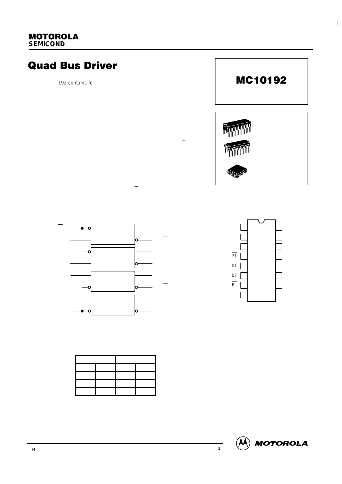
The MC10192 contains four line drivers with complementary outputs. Each
driver has a Data (D) input and shares an Enable
(E) input with another driver.
The two driver outputs are the uncommitted collectors of a pair of NPN
transistors operating as a current switch. Each driver accepts 10K MECL input
signals and provides a nominal signal swing of 800 mV across a 50 Ω load at
each output collector. Outputs can drive higher values of load resistance,
provided that the combination of IR drop and load return voltage VLR does not
cause an output collector to go more negative than –2.4 V with respect to VCC.
To avoid output transistor breakdown, the load return voltage should not be
more positive than +5.5 V with respect to VCC. When the E
input is high, both
output transistors of a driver are nonconducting. When not used, the E
inputs,
as well as the D inputs, may be left open.
Open Collector Outputs Drive Terminated Lines or
Transformers
50 kΩ Input Pulldown Resistors on All Inputs (Unused
Inputs May Be Left Open)
Power Dissipation = 575 mW typ/pkg (No Load)
Propagation Delay= 3.5 ns typ (E
— Output)
3.0 ns typ (D — Output)
LOGIC DIAGRAM
VCC= PIN 16
VEE= PIN 8
E1
7
D1
D2
D3
D4
E2
5
6
10
11
9
3
4
1
2
15
14
13
12
Z1
Z1
Z2
Z2
Z3
Z3
Z4
Z4
TRUTH TABLE
Inputs
Output
E D Z Z
H X H H
L H H L
L L L H
Note: Unused outputs must be terminated
to VCC for proper operation.
DIP
PIN ASSIGNMENT
Z2
Z2
Z1
Z1
D1
D2
E1
V
EE
V
CC
Z3
Z3
Z4
Z4
D4
D3
E2
16
15
14
13
12
11
10
9
1
2
3
4
5
6
7
8
Pin assignment is for Dual–in–Line Package.
For PLCC pin assignment, see the Pin Conversion
T ables on page 6–11 of the Motorola MECL Data
Book (DL122/D).
L SUFFIX
CERAMIC PACKAGE
CASE 620–10
P SUFFIX
PLASTIC PACKAGE
CASE 648–08
FN SUFFIX
PLCC
CASE 775–02
Page 2
MC10192
3–161 MOTOROLAMECL Data
DL122 — Rev 6
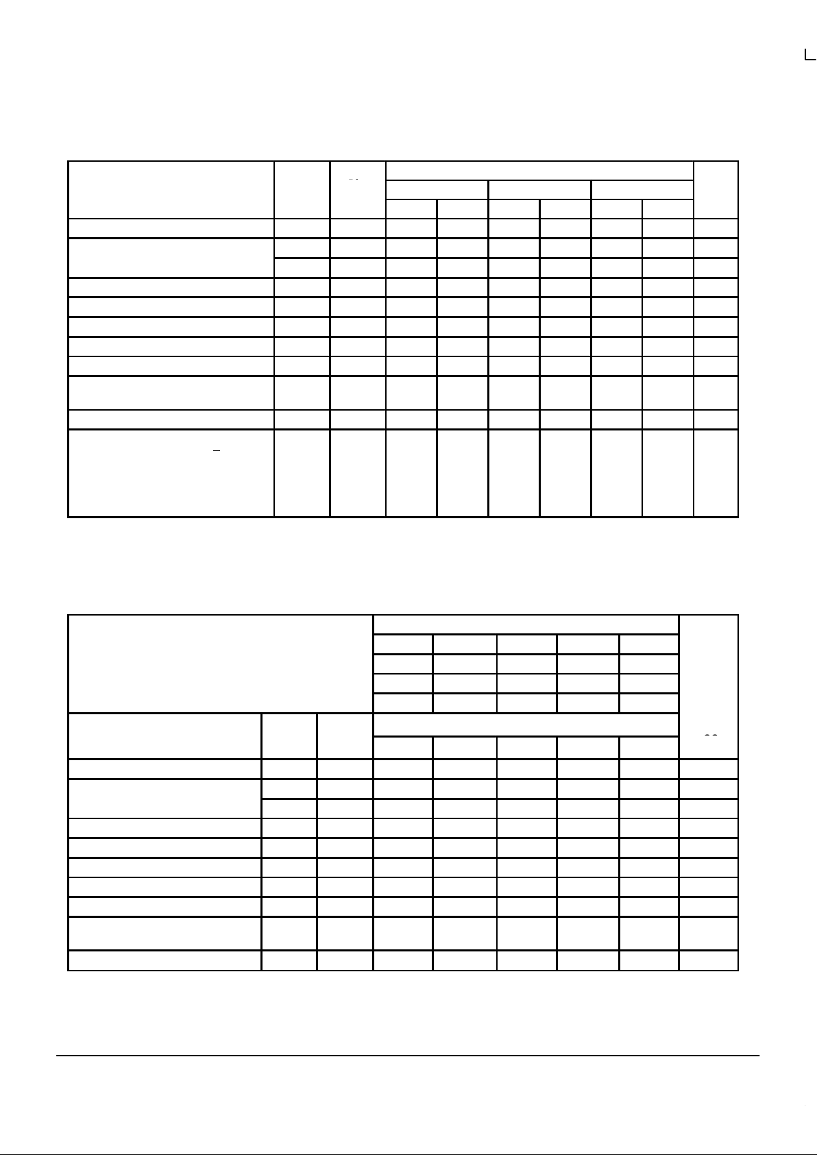
ELECTRICAL CHARACTERISTICS
Test Limits
Pin
Under
–30°C +25°C +85°C
Characteristic Symbol
Under
Test
Min Max Min Max Min Max
Unit
Power Supply Drain Current I
E
8 154 140 154 mAdc
Input Current I
inH
5 350 220 220 µAdc
I
inL
5 0.5 0.5 0.3 µAdc
Output Current High Logic 1 I
OH
2 2.0 mAdc
Output Current Low Logic 0 I
OL
2 13.5 18.0 14.0 18.0 14.0 19.0 mAdc
Threshold Current High Logic 1 I
OHC
2 2.0 2.0 2.0 mAdc
Threshold Current Low Logic 0 I
OLC
2 13.5 14.0 14.0 mAdc
Output Sink Current Low Logic 0 I
OS
2 13.3 13.9 13.3 mAdc
Load Return Voltage Absolute Max
Rating (Note 1.)
V
LR
5.5 5.5 5.5 V
Output Voltage Low (Note 2.) V
OLS
–2.4 V
Switching Times (50Ω Load) ns
Propagation Delay E to Output
D to Output
t
PHL
t
PLH
2.0
1.5
6.0
4.5
Rise/Fall Time (20 to 80%) t
TLH
t
THL
3.3
1. The 5.5V value is a maximum rating, do not exceed. A 270Ω resistor will prevent output transistor breakdown.
2. Limitations of load resistor and load return voltage combinations. Refer to page 3–160 description.
ELECTRICAL CHARACTERISTICS (continued)
TEST VOLTAGE VALUES (Volts)
@ Test Temperature V
IHmax
V
ILmin
V
IHAminVILAmax
V
EE
–30°C –0.890 –1.890 –1.205 –1.500 –5.2
+25°C –0.810 –1.850 –1.105 –1.475 –5.2
+85°C –0.700 –1.825 –1.035 –1.440 –5.2
Pin
TEST VOLTAGE APPLIED TO PINS LISTED BELOW
Characteristic Symbol
Und
er
Test
V
IHmax
V
ILmin
V
IHAminVILAmax
V
EE
(VCC)
Gnd
Power Supply Drain Current I
E
8 8 16
Input Current I
inH
5 5 8 16
I
inL
5 5 8 16
Output Current High Logic 1 I
OH
2 5,6,10,1 1 8 16
Output Current Low Logic 0 I
OL
2 5,6,10,11 8 16
Threshold Current High Logic 1 I
OHC
2 5,7,9,10,1 1 6 8 16
Threshold Current Low Logic 0 I
OLC
5,10,1 1 7,9 6 8 16
Output Sink Current Low Logic 0 I
OS
2 5,6,10,11 8 16
Load Return Voltage Absolute Max
Rating (Note 1.)
V
LR
8 16
Output Voltage Low (Note 2.) V
OLS
8 16
Each MECL 10,000 series circuit has been designed to meet the dc specifications shown in the test table, after thermal equilibrium has been
established. The circuit is in a test socket or mounted on a printed circuit board and transverse air flow greater than 500 linear fpm is maintained.
Outputs are terminated through a 50–ohm resistor to –2.0 volts. Test procedures are shown for only one gate. The other gates are tested in the
same manner.
Page 3

MC10192
MOTOROLA MECL Data
DL122 — Rev 6
3–162
OUTLINE DIMENSIONS
FN SUFFIX
PLASTIC PLCC PACKAGE
CASE 775–02
ISSUE C
NOTES:
1. DATUMS –L–, –M–, AND –N– DETERMINED
WHERE TOP OF LEAD SHOULDER EXITS PLASTIC
BODY AT MOLD PARTING LINE.
2. DIMENSION G1, TRUE POSITION TO BE
MEASURED AT DATUM –T–, SEATING PLANE.
3. DIMENSIONS R AND U DO NOT INCLUDE MOLD
FLASH. ALLOWABLE MOLD FLASH IS 0.010 (0.250)
PER SIDE.
4. DIMENSIONING AND TOLERANCING PER ANSI
Y14.5M, 1982.
5. CONTROLLING DIMENSION: INCH.
6. THE PACKAGE TOP MAY BE SMALLER THAN THE
PACKAGE BOTTOM BY UP TO 0.012 (0.300).
DIMENSIONS R AND U ARE DETERMINED AT THE
OUTERMOST EXTREMES OF THE PLASTIC BODY
EXCLUSIVE OF MOLD FLASH, TIE BAR BURRS,
GATE BURRS AND INTERLEAD FLASH, BUT
INCLUDING ANY MISMATCH BETWEEN THE TOP
AND BOTTOM OF THE PLASTIC BODY.
7. DIMENSION H DOES NOT INCLUDE DAMBAR
PROTRUSION OR INTRUSION. THE DAMBAR
PROTRUSION(S) SHALL NOT CAUSE THE H
DIMENSION TO BE GREATER THAN 0.037 (0.940).
THE DAMBAR INTRUSION(S) SHALL NOT CAUSE
THE H DIMENSION TO BE SMALLER THAN 0.025
(0.635).
–M–
–N–
–L–
Y BRK
W
V
D
D
S
L–M
M
0.007 (0.180) N
S
T
S
L–M
M
0.007 (0.180) N
S
T
S
L–M
S
0.010 (0.250) N
S
T
X
G1
B
U
Z
VIEW D–D
20 1
S
L–M
M
0.007 (0.180) N
S
T
S
L–M
M
0.007 (0.180) N
S
T
S
L–M
S
0.010 (0.250) N
S
T
C
G
VIEW S
E
J
R
Z
A
0.004 (0.100)
–T–
SEATING
PLANE
S
L–M
M
0.007 (0.180) N
S
T
S
L–M
M
0.007 (0.180) N
S
T
H
VIEW S
K
K1
F
G1
DIM MIN MAX MIN MAX
MILLIMETERSINCHES
A 0.385 0.395 9.78 10.03
B 0.385 0.395 9.78 10.03
C 0.165 0.180 4.20 4.57
E 0.090 0.110 2.29 2.79
F 0.013 0.019 0.33 0.48
G 0.050 BSC 1.27 BSC
H 0.026 0.032 0.66 0.81
J 0.020 ––– 0.51 –––
K 0.025 ––– 0.64 –––
R 0.350 0.356 8.89 9.04
U 0.350 0.356 8.89 9.04
V 0.042 0.048 1.07 1.21
W 0.042 0.048 1.07 1.21
X 0.042 0.056 1.07 1.42
Y ––– 0.020 ––– 0.50
Z 2 10 2 10
G1 0.310 0.330 7.88 8.38
K1 0.040 ––– 1.02 –––
____
Page 4

MC10192
3–163 MOTOROLAMECL Data
DL122 — Rev 6
OUTLINE DIMENSIONS
P SUFFIX
PLASTIC DIP PACKAGE
CASE 648–08
ISSUE R
NOTES:
1. DIMENSIONING AND TOLERANCING PER ANSI
Y14.5M, 1982.
2. CONTROLLING DIMENSION: INCH.
3. DIMENSION L TO CENTER OF LEADS WHEN
FORMED PARALLEL.
4. DIMENSION B DOES NOT INCLUDE MOLD FLASH.
5. ROUNDED CORNERS OPTIONAL.
–A–
B
F
C
S
H
G
D
J
L
M
16 PL
SEATING
18
916
K
PLANE
–T–
M
A
M
0.25 (0.010) T
DIM MIN MAX MIN MAX
MILLIMETERSINCHES
A 0.740 0.770 18.80 19.55
B 0.250 0.270 6.35 6.85
C 0.145 0.175 3.69 4.44
D 0.015 0.021 0.39 0.53
F 0.040 0.70 1.02 1.77
G 0.100 BSC 2.54 BSC
H 0.050 BSC 1.27 BSC
J 0.008 0.015 0.21 0.38
K 0.110 0.130 2.80 3.30
L 0.295 0.305 7.50 7.74
M 0 10 0 10
S 0.020 0.040 0.51 1.01
____
L SUFFIX
CERAMIC DIP PACKAGE
CASE 620–10
ISSUE V
NOTES:
1. DIMENSIONING AND TOLERANCING PER
ANSI Y14.5M, 1982.
2. CONTROLLING DIMENSION: INCH.
3. DIMENSION L TO CENTER OF LEAD WHEN
FORMED PARALLEL.
4. DIMENSION F MAY NARROW TO 0.76 (0.030)
WHERE THE LEAD ENTERS THE CERAMIC
BODY.
–A–
–B–
–T–
F
E
G
N
K
C
SEATING
PLANE
16 PLD
S
A
M
0.25 (0.010) T
16 PLJ
S
B
M
0.25 (0.010) T
M
L
DIM MIN MAX MIN MAX
MILLIMETERSINCHES
A 0.750 0.785 19.05 19.93
B 0.240 0.295 6.10 7.49
C ––– 0.200 ––– 5.08
D 0.015 0.020 0.39 0.50
E 0.050 BSC 1.27 BSC
F 0.055 0.065 1.40 1.65
G 0.100 BSC 2.54 BSC
H 0.008 0.015 0.21 0.38
K 0.125 0.170 3.18 4.31
L 0.300 BSC 7.62 BSC
M 0 15 0 15
N 0.020 0.040 0.51 1.01
____
16 9
18
Motorola reserves the right to make changes without further notice to any products herein. Motorola makes no warranty , representation or guarantee regarding
the suitability of its products for any particular purpose, nor does Motorola assume any liability arising out of the application or use of any product or circuit, and
specifically disclaims any and all liability, including without limitation consequential or incidental damages. “T ypical” parameters which may be provided in Motorola
data sheets and/or specifications can and do vary in different applications and actual performance may vary over time. All operating parameters, including “Typicals”
must be validated for each customer application by customer’s technical experts. Motorola does not convey any license under its patent rights nor the rights of
others. Motorola products are not designed, intended, or authorized for use as components in systems intended for surgical implant into the body, or other
applications intended to support or sustain life, or for any other application in which the failure of the Motorola product could create a situation where personal injury
or death may occur. Should Buyer purchase or use Motorola products for any such unintended or unauthorized application, Buyer shall indemnify and hold Motorola
and its officers, employees, subsidiaries, affiliates, and distributors harmless against all claims, costs, damages, and expenses, and reasonable attorney fees
arising out of, directly or indirectly, any claim of personal injury or death associated with such unintended or unauthorized use, even if such claim alleges that
Motorola was negligent regarding the design or manufacture of the part. Motorola and are registered trademarks of Motorola, Inc. Motorola, Inc. is an Equal
Opportunity/Affirmative Action Employer.
How to reach us:
USA/EUROPE/Locations Not Listed: Motorola Literature Distribution; JAPAN: Nippon Motorola Ltd.; Tatsumi–SPD–JLDC, 6F Seibu–Butsuryu–Center,
P.O. Box 5405, Denver, Colorado 80217. 303–675–2140 or 1–800–441–2447 3–14–2 Tatsumi Koto–Ku, To kyo 135, Japan. 81–3–3521–8315
Mfax: RMFAX0@email.sps.mot.com – TOUCHT ONE 602–244–6609 ASIA/PACIFIC: Motorola Semiconductors H.K. Ltd.; 8B Tai Ping Industrial Park,
INTERNET: http://Design–NET.com 51 Ting Kok Road, Tai Po, N.T., Hong Kong. 852–26629298
MC10192/D
*MC10192/D*
◊
 Loading...