

Page 1
SEMICONDUCTOR TECHNICAL DATA
3–69
REV 6
Motorola, Inc. 1996
9/96
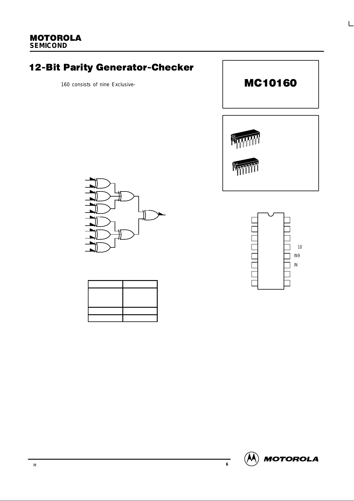
The MC10160 consists of nine Exclusive-OR gates in a single package,
internally connected to provide odd parity checking or generation. Output goes
high when an odd number of inputs are high. Unconnected inputs are pulled to
low logic levels allowing parity detection and generation for less than 12 bits.
PD= 320 mW typ/pkg (No Load)
tpd= 5.0 ns typ
tr, tf= 2.0 ns typ (20%–80%)
LOGIC DIAGRAM
V
CC1
= PIN 1
V
CC2
= PIN 16
VEE= PIN 8
15
14
13
12
11
10
9
7
6
5
4
3
2
INPUT OUTPUT
Sum of
High Level
Inputs
Pin 2
Even Low
Odd High
V
CC1
OUT
IN1
IN2
IN3
IN4
IN5
V
EE
V
CC2
IN12
IN11
IN10
IN9
IN8
IN7
IN6
16
15
14
13
12
11
10
9
1
2
3
4
5
6
7
8
PIN ASSIGNMENT
L SUFFIX
CERAMIC PACKAGE
CASE 620–10
P SUFFIX
PLASTIC PACKAGE
CASE 648–08
Page 2
MC10160
MOTOROLA MECL Data
DL122 — Rev 6
3–70
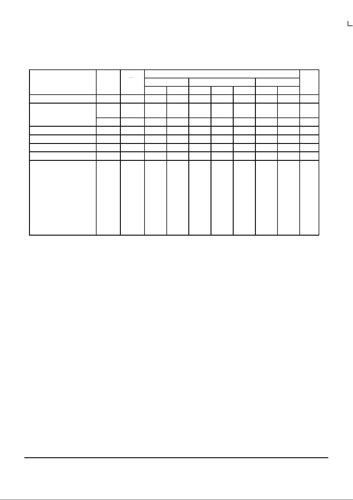
ELECTRICAL CHARACTERISTICS
Test Limits
Pin
Under
–30°C +25°C +85°C
Characteristic Symbol
Under
Test
Min Max Min Typ Max Min Max
Unit
Power Supply Drain Current I
E
8 86 62 78 86 mAdc
Input Current I
inH
(Note 1.)
3
4
425
350
265
220
265
220
µAdc
I
inL
3 0.5 0.5 0.3 µAdc
Output Voltage Logic 1 V
OH
2 –1.060 –0.890 –0.960 –0.810 –0.890 –0.700 Vdc
Output Voltage Logic 0 V
OL
2 –1.890 –1.675 –1.850 –1.650 –1.825 –1.615 Vdc
Threshold Voltage Logic 1 V
OHA
2 –1.080 –0.980 –0.910 Vdc
Threshold Voltage Logic 0 V
OLA
2 –1.655 –1.630 –1.595 Vdc
Switching Times (50Ω Load) ns
Propagation Delay t
3+2+
t
3+2–
t
3–2–
t
3–2+
t
4+2+
t
4+2–
t
4–2–
t
4–2+
2
2
2
2
2
2
2
2
1.8
1.8
1.8
1.8
1.8
1.8
1.8
1.8
8.1
8.1
8.1
8.1
8.1
8.1
8.1
8.1
2.0
2.0
2.0
2.0
2.0
2.0
2.0
2.0
5.0
5.0
5.0
5.0
5.0
5.0
5.0
5.0
7.5
7.5
7.5
7.5
7.5
7.5
7.5
7.5
2.0
2.0
2.0
2.0
2.0
2.0
2.0
2.0
8.0
8.0
8.0
8.0
8.0
8.0
8.0
8.0
Rise Time (20 to 80%) t
2+
2 1.1 3.5 1.1 2.0 3.3 1.0 3.5
Fall Time (20 to 80%) t
2–
2 1.1 3.5 1.1 2.0 3.3 1.0 3.5
1. Pins 3, 6, 7, 11, 12, 15 are similar. Pins 4, 5, 9, 10, 13, 14 are similar.
Page 3

MC10160
3–71 MOTOROLAMECL Data
DL122 — Rev 6
ELECTRICAL CHARACTERISTICS (continued)
TEST VOLTAGE VALUES (Volts)
@ Test Temperature V
IHmax
V
ILmin
V
IHAminVILAmax
V
EE
–30°C –0.890 –1.890 –1.205 –1.500 –5.2
+25°C –0.810 –1.850 –1.105 –1.475 –5.2
+85°C –0.700 –1.825 –1.035 –1.440 –5.2
Pin
TEST VOLTAGE APPLIED TO PINS LISTED BELOW
Characteristic Symbol
Und
er
Test
V
IHmax
V
ILmin
V
IHAminVILAmax
V
EE
(VCC)
Gnd
Power Supply Drain Current I
E
8
4,5,9,
10,13,14
8 1,16
Input Current I
inH
(Note 1.)
3
4
3
4
8
8
1,16
1,16
I
inL
3 3 8 1,16
Output Voltage Logic 1 V
OH
2 3
4,5,6,7,9,10,
11,12,13,14,15
8 1,16
Output Voltage Logic 0 V
OL
2
3,4,5,6,7,9,10,
11,12,13,14,15
8 1,16
Threshold Voltage Logic 1 V
OHA
2
4,5,6,7,9,10,
11,12,13,14,15
3 8 1,16
Threshold Voltage Logic 0 V
OLA
2
3,5,6,7,9,10,
11,12,13,14,15
4 8 1,16
Switching Times (50Ω Load) +1.11V Pulse In Pulse Out –3.2 V +2.0 V
Propagation Delay t
3+2+
t
3+2–
t
3–2–
t
3–2+
t
4+2+
t
4+2–
t
4–2–
t
4–2+
2
2
2
2
2
2
2
2
4
4
3
3
3
3
3
3
4
4
4
4
2
2
2
2
2
2
2
2
8
8
8
8
8
8
8
8
1,16
1,16
1,16
1,16
1,16
1,16
1,16
1,16
Rise Time (20 to 80%) t
2+
2 3 2 8 1,16
Fall Time (20 to 80%) t
2–
2 3 2 8 1,16
1. Pins 3, 6, 7, 11, 12, 15 are similar. Pins 4, 5, 9, 10, 13, 14 are similar.
Each MECL 10,000 series circuit has been designed to meet the dc specifications shown in the test table, after thermal equilibrium has been
established. The circuit is in a test socket or mounted on a printed circuit board and transverse air flow greater than 500 linear fpm is maintained.
Outputs are terminated through a 50–ohm resistor to –2.0 volts. Test procedures are shown for only one gate. The other gates are tested in the
same manner.
Page 4

MC10160
MOTOROLA MECL Data
DL122 — Rev 6
3–72
OUTLINE DIMENSIONS
P SUFFIX
PLASTIC DIP PACKAGE
CASE 648–08
ISSUE R
NOTES:
1. DIMENSIONING AND TOLERANCING PER ANSI
Y14.5M, 1982.
2. CONTROLLING DIMENSION: INCH.
3. DIMENSION L TO CENTER OF LEADS WHEN
FORMED PARALLEL.
4. DIMENSION B DOES NOT INCLUDE MOLD FLASH.
5. ROUNDED CORNERS OPTIONAL.
–A–
B
F
C
S
H
G
D
J
L
M
16 PL
SEATING
18
916
K
PLANE
–T–
M
A
M
0.25 (0.010) T
DIM MIN MAX MIN MAX
MILLIMETERSINCHES
A 0.740 0.770 18.80 19.55
B 0.250 0.270 6.35 6.85
C 0.145 0.175 3.69 4.44
D 0.015 0.021 0.39 0.53
F 0.040 0.70 1.02 1.77
G 0.100 BSC 2.54 BSC
H 0.050 BSC 1.27 BSC
J 0.008 0.015 0.21 0.38
K 0.110 0.130 2.80 3.30
L 0.295 0.305 7.50 7.74
M 0 10 0 10
S 0.020 0.040 0.51 1.01
____
L SUFFIX
CERAMIC DIP PACKAGE
CASE 620–10
ISSUE V
NOTES:
1. DIMENSIONING AND TOLERANCING PER
ANSI Y14.5M, 1982.
2. CONTROLLING DIMENSION: INCH.
3. DIMENSION L TO CENTER OF LEAD WHEN
FORMED PARALLEL.
4. DIMENSION F MAY NARROW TO 0.76 (0.030)
WHERE THE LEAD ENTERS THE CERAMIC
BODY.
–A–
–B–
–T–
F
E
G
N
K
C
SEATING
PLANE
16 PLD
S
A
M
0.25 (0.010) T
16 PLJ
S
B
M
0.25 (0.010) T
M
L
DIM MIN MAX MIN MAX
MILLIMETERSINCHES
A 0.750 0.785 19.05 19.93
B 0.240 0.295 6.10 7.49
C ––– 0.200 ––– 5.08
D 0.015 0.020 0.39 0.50
E 0.050 BSC 1.27 BSC
F 0.055 0.065 1.40 1.65
G 0.100 BSC 2.54 BSC
H 0.008 0.015 0.21 0.38
K 0.125 0.170 3.18 4.31
L 0.300 BSC 7.62 BSC
M 0 15 0 15
N 0.020 0.040 0.51 1.01
____
16 9
18
Motorola reserves the right to make changes without further notice to any products herein. Motorola makes no warranty , representation or guarantee regarding
the suitability of its products for any particular purpose, nor does Motorola assume any liability arising out of the application or use of any product or circuit, and
specifically disclaims any and all liability, including without limitation consequential or incidental damages. “T ypical” parameters which may be provided in Motorola
data sheets and/or specifications can and do vary in different applications and actual performance may vary over time. All operating parameters, including “Typicals”
must be validated for each customer application by customer’s technical experts. Motorola does not convey any license under its patent rights nor the rights of
others. Motorola products are not designed, intended, or authorized for use as components in systems intended for surgical implant into the body, or other
applications intended to support or sustain life, or for any other application in which the failure of the Motorola product could create a situation where personal injury
or death may occur. Should Buyer purchase or use Motorola products for any such unintended or unauthorized application, Buyer shall indemnify and hold Motorola
and its officers, employees, subsidiaries, affiliates, and distributors harmless against all claims, costs, damages, and expenses, and reasonable attorney fees
arising out of, directly or indirectly, any claim of personal injury or death associated with such unintended or unauthorized use, even if such claim alleges that
Motorola was negligent regarding the design or manufacture of the part. Motorola and are registered trademarks of Motorola, Inc. Motorola, Inc. is an Equal
Opportunity/Affirmative Action Employer.
How to reach us:
USA/EUROPE/Locations Not Listed: Motorola Literature Distribution; JAPAN: Nippon Motorola Ltd.; Tatsumi–SPD–JLDC, 6F Seibu–Butsuryu–Center,
P.O. Box 5405, Denver, Colorado 80217. 303–675–2140 or 1–800–441–2447 3–14–2 Tatsumi Koto–Ku, Tokyo 135, Japan. 81–3–3521–8315
Mfax: RMFAX0@email.sps.mot.com – TOUCHT ONE 602–244–6609 ASIA/PACIFIC: Motorola Semiconductors H.K. Ltd.; 8B Tai Ping Industrial Park,
INTERNET: http://Design–NET.com 51 Ting Kok Road, Tai Po, N.T., Hong Kong. 852–26629298
MC10160/D
*MC10160/D*
◊
 Loading...