

Page 1
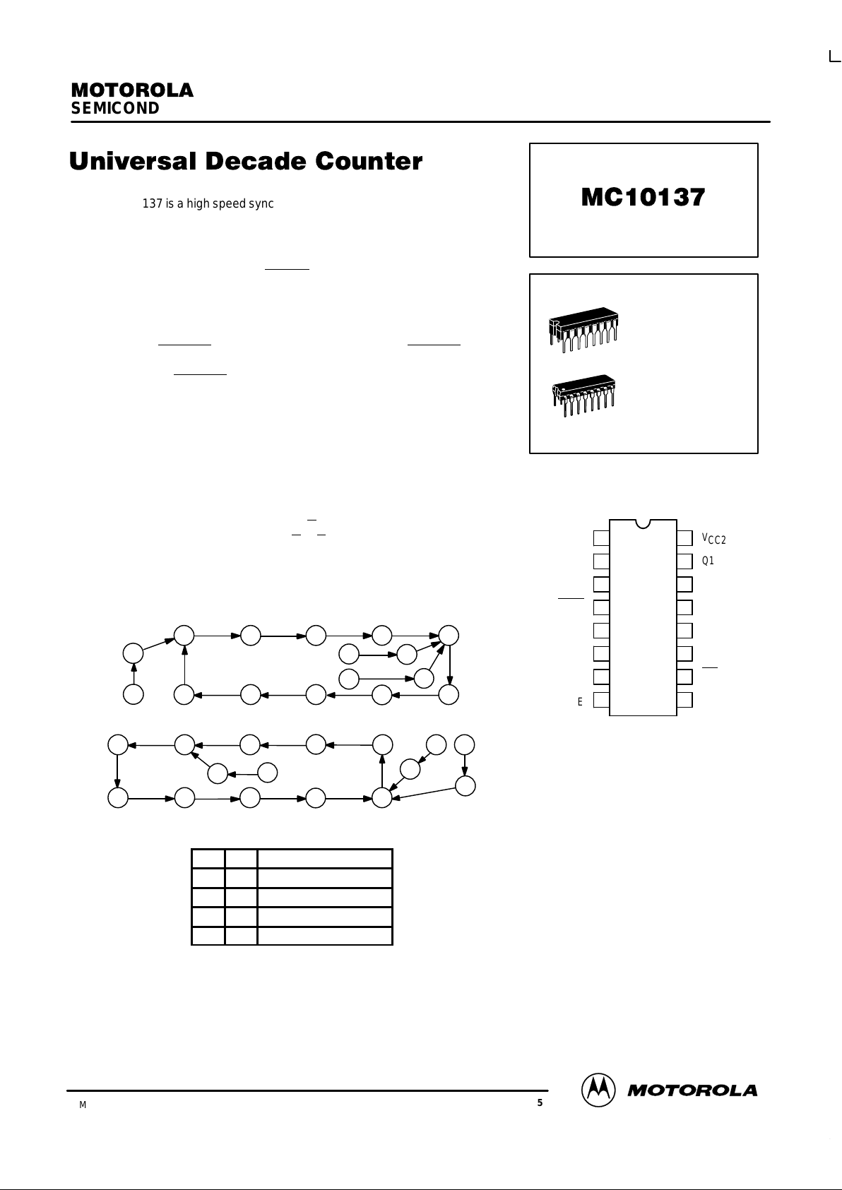
STATE DIAGRAMS
987
6
5
11
13
12
10
14
15
012
3
4
012
3
4
987
6
5
13
12
10
11
14
COUNT UP
COUNT DOWN
15
SEMICONDUCTOR TECHNICAL DATA
3–35
REV 5
Motorola, Inc. 1996
3/93
The MC10137 is a high speed synchronous counter that can count up, down,
preset, or stop count at frequencies exceeding 100 MHz. The flexibility of this
device allows the designer to use one basic counter for most applications. The
synchronous count feature makes the MC10137 suitable for either computers
or instrumentation.
Three control lines (S1, S2, and Carry In
) determine the operation mode of
the counter. Lines S1 and S2 determine one of four operations; preset
(program), increment (count up), decrement (count down), or hold (stop count).
Note that in the preset mode a clock pulse is necessary to load the counter, and
the information present on the data inputs (D0, D1, D2, and D3) will be entered
into the counter. Carry Out
goes low on the terminal count. The Carry Out on the
MC10137 is partially decoded from Q1 and Q2 directly, so in the preset mode
the condition of the Carry Out
after the Clock’s positive excursion will depend on
the condition of Q1 and/or Q2. The counter changes state only on the positive
going edge of the clock. Any other input may change at any time except during
the positive transition of the clock. The sequence for counting out of improper
states is as shown in the State Diagrams.
PD= 625 mW typ/pkg (No Load)
f
count
= 150 MHz typ
tpd= 3.3 ns typ (C–Q)
= 7.0 ns typ (C–C
out
)
= 5.0 ns typ (C
in–Cout
)
FUNCTION SELECT TABLE
S1 S2 Operating Mode
L L Preset (Program)
L H Increment (Count Up)
H L Decrement (Count Down)
H H Hold (Stop Count)
PIN ASSIGNMENT
V
CC1
2
3
C
OUT
D3
D2
S2
V
EE
V
CC2
Q1
Q0
C
D0
D1
C
IN
S1
16
15
14
13
12
11
10
9
1
2
3
4
5
6
7
8
L SUFFIX
CERAMIC PACKAGE
CASE 620–10
P SUFFIX
PLASTIC PACKAGE
CASE 648–08
Page 2

MC10137
MOTOROLA MECL Data
DL122 — Rev 6
3–36
LOGIC DIAGRAM
NOTE: Flip–flops will toggle when all T inputs are low.
V
CC1
= PIN 1
V
CC2
= PIN 16
VEE= PIN 8
Q2
K
T
J
T
J
T T
Q3
T
Q3
Q1
Q1
T
T
C
J
C
T
C
Q0
S1 9
S2 7
Carry In
10
13
Clock
12 D0
14 Q0
11 D1 15 Q1
6D2
2Q2
5D3
3Q3
4 Carry Out
T
C
Q0
T
Q2
J
T
SEQUENTIAL TRUTH TABLE*
INPUTS OUTPUTS
S1 S2 D0 D1 D2 D3
Carry
In
Clock
**
Q0 Q1 Q2 Q3
Carry
Out
L L H H H L X H H H H L H
L H X X X X L H L L L H H
L H X X X X L H H L L H L
L H X X X X L H L L L L H
L H X X X X L H H L L L H
L H X X X X H L H L L L H
L H X X X X H H H L L L H
H H X X X X X H H L L L H
L L H H L L X H H H L L H
H L X X X X L H L H L L H
H L X X X X L H H L L L H
H L X X X X L H L L L L L
* Truth table shows logic states assuming inputs vary in sequence shown from top to bottom.
** A clock H is defined as a clock input transition from a low to a high logic level.
Page 3

MC10137
3–37 MOTOROLAMECL Data
DL122 — Rev 6
ELECTRICAL CHARACTERISTICS
Test Limits
Pin
Under
–30°C +25°C +85°C
Characteristic Symbol
Under
Test
Min Max Min Typ Max Min Max
Unit
Power Supply Drain Current I
E
8 165 120 150 165 mAdc
Input Current I
inH
5,6,11,12
7
9,10
13
350
425
390
460
220
265
245
290
220
265
245
290
µAdc
I
inL
All 0.5 0.5 0.3 µAdc
Output Voltage Logic 1 V
OH
14 (2.) –1.060 –0.890 –0.960 –0.810 –0.890 –0.700 Vdc
Output Voltage Logic 0 V
OL
14 (2.) –1.890 –1.675 –1.850 –1.650 –1.825 –1.615 Vdc
Threshold Voltage Logic 1 V
OHA
14 (2.) –1.080 –0.980 –0.910 Vdc
Threshold Voltage Logic 0 V
OLA
14 (2.) –1.655 –1.630 –1.595 Vdc
Switching Times (50Ω Load) ns
Propagation Delay Clock Input t
13+14+
t
13+14–
t
13+4+
t
13+4–
14
14
4
4
0.8
0.8
2.0
2.0
4.8
4.8
10.9
10.9
1.0
1.0
2.5
2.5
3.3
3.3
7.0
7.0
4.5
4.5
10.5
10.5
1.1
1.1
2.4
2.4
5.0
5.0
11.5
11.5
Carry In to Carry Out t
10–4–
t
10+4+
4 (3.)
4
1.6
1.6
7.4
7.4
1.6
1.6
5.0
5.0
6.9
6.9
1.9
1.9
7.5
7.5
Setup Time Data Inputs t
12+13+
t
12–13+
14
14
3.5
3.5
3.5
3.5
3.5
3.5
Select Inputs t
9+13+
t
7+13+
14
14
7.5
7.5
7.5
7.5
7.5
7.5
Carry In Input t
10–13+
t
13+10+
14
14
4.5
–1.0
3.7
–1.0
4.5
–1.0
Hold Time Data Inputs t
13+12+
t
13+12–
14
14
0
0
0
0
0
0
Select Inputs t
13+9+
t
13+7+
14
14
–2.5
–2.5
–2.5
–2.5
–2.5
–2.5
Carry In Input t
13+10–
t
10+13+
14
14
–1.6
4.0
–1.6
3.1
–1.6
4.0
Counting Frequency f
countup
f
countdown
14
14
125
125
125
125
150
150
125
125
MHz
Rise Time (20 to 80%) t
4+
t
14+
4
14
0.9
0.9
3.3
3.3
1.1
1.1
2.0
2.0
3.3
3.3
1.1
1.1
3.5
3.5
ns
Fall Time (20 to 80%) t
4–
t
14–
4
14
0.9
0.9
3.3
3.3
1.1
1.1
2.0
2.0
3.3
3.3
1.1
1.1
3.5
3.5
1. Individually apply V
ILmin
to pin under test.
2. Measure output after clock pulse
V
IH
V
IL
appears at clock input (Pin 13).
3. Before test set Q1 and Q2 outputs to a logic low.
Page 4

MC10137
MOTOROLA MECL Data
DL122 — Rev 6
3–38
ELECTRICAL CHARACTERISTICS (continued)
TEST VOLTAGE VALUES (Volts)
@ Test Temperature V
IHmax
V
ILminVIHAminVILAmax
V
EE
–30°C –0.890 –1.890 –1.205 –1.500 –5.2
+25°C –0.810 –1.850 –1.105 –1.475 –5.2
+85°C –0.700 –1.825 –1.035 –1.440 –5.2
Pin
TEST VOLTAGE APPLIED TO PINS LISTED BELOW
Characteristic Symbol
Und
er
Test
V
IHmax
V
ILminVIHAminVILAmax
V
EE
(VCC)
Gnd
Power Supply Drain Current I
E
8 8 1, 16
Input Current I
inH
5,6,11,12
7
9,10
13
5,6,11,12
7
9,10
13
8
8
8
8
1, 16
1, 16
1, 16
1, 16
I
inL
All Note 1. 8 1, 16
Output Voltage Logic 1 V
OH
14 (2.) 12 7, 9 8 1, 16
Output Voltage Logic 0 V
OL
14 (2.) 7, 9 8 1, 16
Threshold Voltage Logic 1 V
OHA
14 (2.) 7, 9 12 8 1, 16
Threshold Voltage Logic 0 V
OLA
14 (2.) 7, 9 12 8 1, 16
Switching Times (50Ω Load) +1.1 1V +0.31V Pulse In Pulse Out –3.2 V +2.0 V
Propagation Delay Clock Input t
13+14+
t
13+14–
t
13+4+
t
13+4–
14
14
4
4
12
7
7
13
13
13
13
14
14
4
4
8
8
8
8
1, 16
1, 16
1, 16
1, 16
Carry In to Carry Out t
10–4–
t
10+4+
4 (3.)
4
7
7
13
13
10
10
4
4
8
8
1, 16
1, 16
Setup Time Data Inputs t
12+13+
t
12–13+
14
14
7, 9
7, 9
12, 13
12, 13
14
14
8
8
1, 16
1, 16
Select Inputs t
9+13+
t
7+13+
14
14
9, 13
7, 13
14
14
8
8
1, 16
1, 16
Carry In Inputs t
10–13+
t
13+10+
14
14
7
7
9
9
10, 13
10, 13
14
14
8
8
1, 16
1, 16
Hold Time Data Inputs t
13+12+
t
13+12–
14
14
7, 9
7, 9
12, 13
12, 13
14
14
8
8
1, 16
1, 16
Select Inputs t
13+9+
t
13+7+
14
14
9, 13
7, 13
14
14
8
8
1, 16
1, 16
Carry In Inputs t
13+10–
t
10+13+
14
14
7
7
9
9
10, 13
10, 13
14
14
8
8
1, 16
1, 16
Counting Frequency f
countup
f
countdown
14
14
7
9
13
13
14
14
8
8
1, 16
1, 16
Rise Time (20 to 80%) t
4+
t
14+
4
14
7
7
13
13
4
14
8
8
1, 16
1, 16
Fall Time (20 to 80%) t
4–
t
14–
4
14
7
7
13
13
4
14
8
8
1, 16
1, 16
1. Individually test each input; apply V
ILmin
to pin under test.
2. Measure output after clock pulse
V
IH
V
IL
appears at clock input (Pin 13).
3. Before test set all Q outputs to a logic high.
Each MECL 10,000 series circuit has been designed to meet the dc specifications shown in the test table, after thermal equilibrium has been
established. The circuit is in a test socket or mounted on a printed circuit board and transverse air flow greater than 500 linear fpm is maintained.
Outputs are terminated through a 50-ohm resistor to –2.0 volts. Test procedures are shown for only one gate. The other gates are tested in the
same manner.
Page 5

MC10137
3–39 MOTOROLAMECL Data
DL122 — Rev 6
Clock Input
Q
D or S
C
Clock
Q Output
SWITCHING TIME TEST CIRCUIT AND WAVEFORMS @ 25°C
(a) is the minimum time to wait after the
counter has been enabled to clock it.
(b) is the minimum time before the counter
has been disabled that it may be clocked.
(c) is the minimum time before the counter
is enabled that a clock pulse may be
applied with no effect on the state of the
counter.
(d) is the minimum time to wait after the
counter is disabled that a clock pulse may
be applied with no effect in the state of the
counter.
(b) and (c) may be negative numbers.
C
in
TP
out
Coax
C
out
Q3
Q2
Q1
Q0
C
D0
D1
D2
D3
S1
S2
V
out
V
in
Coax
TP
in
16
25
µ
F
1
0.1
µ
F
8
VEE = –3.2 Vdc
V
CC1
= V
CC2
= +2.0 Vdc
0.1
µ
F
t
setup L
t
hold L
50%
t
hold H
t
setup H
50%
50%
t
C+Q+
t
Q+
80%
50%
20%
t
Q–
t
C+Q–
+0.31 V
+1.11 V
+0.31 V
+1.11 V
50-ohm termination to ground located in each scope channel input.
All input and output cables to the
scope are equal lengths of 50-ohm
coaxial cable. Wire length should be
< 1/4 inch from TPin to input pin and
TP
out
to output pin.
Unused outputs are connected to a
50-ohm resistor to ground.
NOTE:
t
setup
is the minimum time before the positive
transition of the clock pulse (C) that information must
be present at the input D or S.
t
hold
is the minimum time after the positive
transition of the clock pulse (C) that information must
remain unchanged at the input D or S.
Input Pulse
t+ = t– = 2.0
±
0.2 ns
(20 to 80%)
Clock
Carry in
(c)
(d)
Clock
Carry In
(a)
(b)
Page 6

MC10137
MOTOROLA MECL Data
DL122 — Rev 6
3–40
OUTLINE DIMENSIONS
P SUFFIX
PLASTIC DIP PACKAGE
CASE 648–08
ISSUE R
NOTES:
1. DIMENSIONING AND TOLERANCING PER ANSI
Y14.5M, 1982.
2. CONTROLLING DIMENSION: INCH.
3. DIMENSION L TO CENTER OF LEADS WHEN
FORMED PARALLEL.
4. DIMENSION B DOES NOT INCLUDE MOLD FLASH.
5. ROUNDED CORNERS OPTIONAL.
–A–
B
F
C
S
H
G
D
J
L
M
16 PL
SEATING
18
916
K
PLANE
–T–
M
A
M
0.25 (0.010) T
DIM MIN MAX MIN MAX
MILLIMETERSINCHES
A 0.740 0.770 18.80 19.55
B 0.250 0.270 6.35 6.85
C 0.145 0.175 3.69 4.44
D 0.015 0.021 0.39 0.53
F 0.040 0.70 1.02 1.77
G 0.100 BSC 2.54 BSC
H 0.050 BSC 1.27 BSC
J 0.008 0.015 0.21 0.38
K 0.110 0.130 2.80 3.30
L 0.295 0.305 7.50 7.74
M 0 10 0 10
S 0.020 0.040 0.51 1.01
____
L SUFFIX
CERAMIC DIP PACKAGE
CASE 620–10
ISSUE V
NOTES:
1. DIMENSIONING AND TOLERANCING PER
ANSI Y14.5M, 1982.
2. CONTROLLING DIMENSION: INCH.
3. DIMENSION L TO CENTER OF LEAD WHEN
FORMED PARALLEL.
4. DIMENSION F MAY NARROW TO 0.76 (0.030)
WHERE THE LEAD ENTERS THE CERAMIC
BODY.
–A–
–B–
–T–
F
E
G
N
K
C
SEATING
PLANE
16 PLD
S
A
M
0.25 (0.010) T
16 PLJ
S
B
M
0.25 (0.010) T
M
L
DIM MIN MAX MIN MAX
MILLIMETERSINCHES
A 0.750 0.785 19.05 19.93
B 0.240 0.295 6.10 7.49
C ––– 0.200 ––– 5.08
D 0.015 0.020 0.39 0.50
E 0.050 BSC 1.27 BSC
F 0.055 0.065 1.40 1.65
G 0.100 BSC 2.54 BSC
H 0.008 0.015 0.21 0.38
K 0.125 0.170 3.18 4.31
L 0.300 BSC 7.62 BSC
M 0 15 0 15
N 0.020 0.040 0.51 1.01
____
16 9
18
Motorola reserves the right to make changes without further notice to any products herein. Motorola makes no warranty , representation or guarantee regarding
the suitability of its products for any particular purpose, nor does Motorola assume any liability arising out of the application or use of any product or circuit, and
specifically disclaims any and all liability, including without limitation consequential or incidental damages. “T ypical” parameters which may be provided in Motorola
data sheets and/or specifications can and do vary in different applications and actual performance may vary over time. All operating parameters, including “Typicals”
must be validated for each customer application by customer’s technical experts. Motorola does not convey any license under its patent rights nor the rights of
others. Motorola products are not designed, intended, or authorized for use as components in systems intended for surgical implant into the body, or other
applications intended to support or sustain life, or for any other application in which the failure of the Motorola product could create a situation where personal injury
or death may occur. Should Buyer purchase or use Motorola products for any such unintended or unauthorized application, Buyer shall indemnify and hold Motorola
and its officers, employees, subsidiaries, affiliates, and distributors harmless against all claims, costs, damages, and expenses, and reasonable attorney fees
arising out of, directly or indirectly, any claim of personal injury or death associated with such unintended or unauthorized use, even if such claim alleges that
Motorola was negligent regarding the design or manufacture of the part. Motorola and are registered trademarks of Motorola, Inc. Motorola, Inc. is an Equal
Opportunity/Affirmative Action Employer.
How to reach us:
USA/EUROPE/Locations Not Listed: Motorola Literature Distribution; JAPAN: Nippon Motorola Ltd.; Tatsumi–SPD–JLDC, 6F Seibu–Butsuryu–Center,
P.O. Box 20912; Phoenix, Arizona 85036. 1–800–441–2447 or 602–303–5454 3–14–2 Tatsumi Koto–Ku, Tokyo 135, Japan. 03–81–3521–8315
MFAX: RMF AX0@email.sps.mot.com – T OUCHTONE 602–244–6609 ASIA/PACIFIC: Motorola Semiconductors H.K. Ltd.; 8B Tai Ping Industrial Park,
INTERNET: http://Design–NET .com 51 T ing Kok Road, Tai Po, N.T., Hong Kong. 852–26629298
MC10137/D
*MC10137/D*
◊
 Loading...