

Page 1
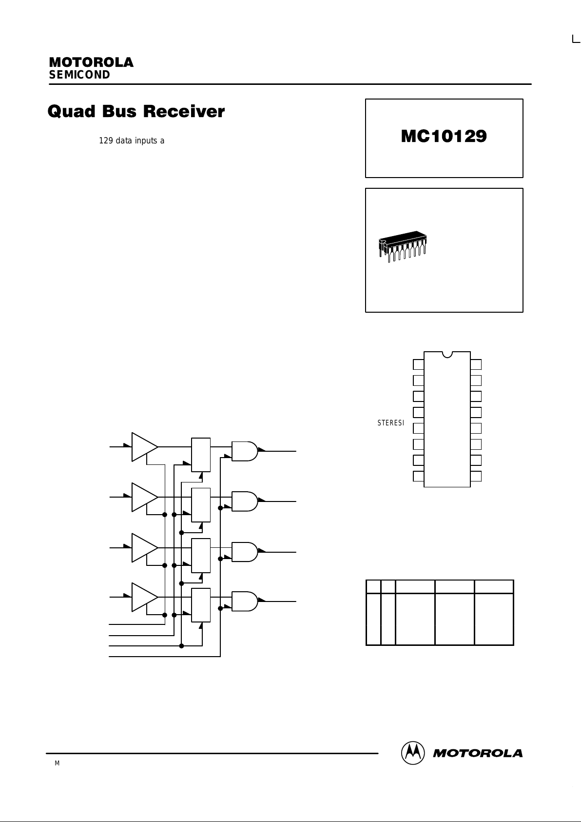
LOGIC DIAGRAM
VCC = PIN 9
GND = PIN 1 AND 16
VEE = PIN 8
14 Q0
D0 7
D
C
R
15 Q1
D1 13
D
C
R
3Q2
D2 6
D
C
R
2Q3
D3 4
D
C
R
HYSTERESIS
CONTROL 5
CLOCK 11
RESET 10
STROBE 12
SEMICONDUCTOR TECHNICAL DATA
3–1
REV 6
Motorola, Inc. 1996
9/96
The MC10129 data inputs are compatible with, and accept TTL logic levels
as well as levels compatible with IBM–type buses. The clock, strobe, and reset
inputs accept MECL 10,000 logic levels.
The data inputs accept the bus levels, and storage elements are provided to
yield temporary latch storage of the information after receiving it from the bus.
The outputs can be strobed to allow accurate synchronization of signals and/or
connection to MECL 10,000 level buses. When the clock is low, and the reset
input is disabled, the outputs will follow the D inputs. The latches will store the
data on the rising edge of the clock. The outputs are enabled when the strobe
input is high. Unused D inputs must be tied to VCC or Gnd. The clock, strobe,
and reset inputs each have 50 k ohm pulldown resistors to VEE. They may be
left floating, if not used.
The MC10129 will operate in either of two modes. The first mode is obtained
by tying the hysteresis control input to VEE. In this mode, the input threshold
points of the D inputs are fixed. The second mode is obtained by tying the
hysteresis control input to ground. In this mode, input hysteresis is achieved as
shown in the test table. This hysteresis is desirable where extra noise margin is
required on the D inputs. The outer input pins are unaffected by the mode of
operation used.
The MC10129 is especially useful in interface applications for central
processors, mini–computers, and peripheral equipment.
PD= 750 mW typ/pkg (No Load)
tpd= 10 ns typ
VCC Max = 7.0 Vdc
TRUTH TABLE
D C STROBE RESET Qn +
1
X X L X L
X H X H L
L L H X L
X H H L Q
n
H L H X H
PIN ASSIGNMENT
GND
Q3
Q2
D3
HYSTERESIS
CONTROL
D2
D0
V
EE
GND
Q1
Q0
D1
STROBE
CLOCK
RESET
V
CC
16
15
14
13
12
11
10
9
1
2
3
4
5
6
7
8
L SUFFIX
CERAMIC PACKAGE
CASE 620–10
Page 2
MC10129
MOTOROLA MECL Data
DL122 — Rev 6
3–2
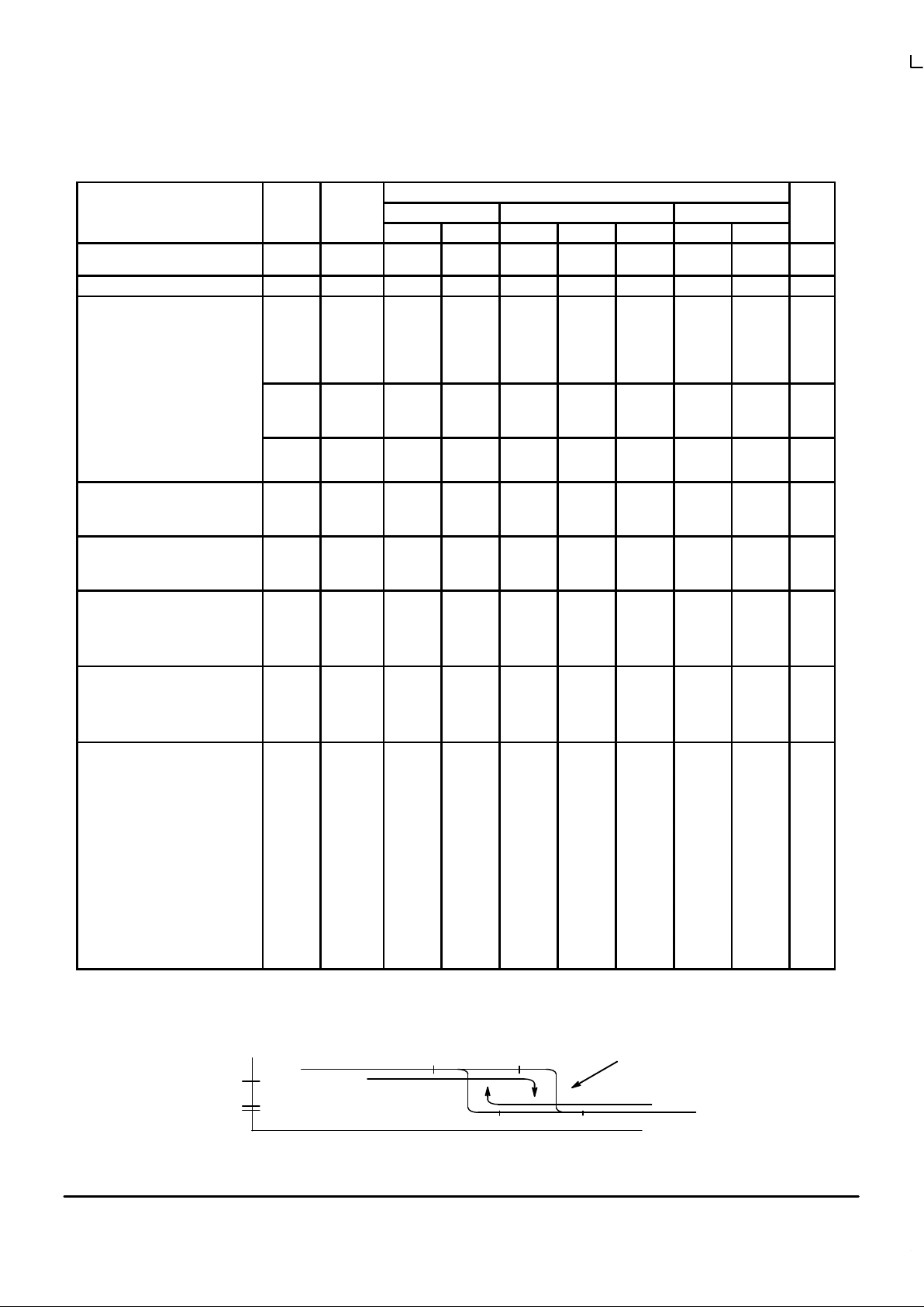
ELECTRICAL CHARACTERISTICS
Test Limits
Pin
Under
–30°C +25°C +85°C
Characteristic Symbol
Under
Test
Min Max Min Typ Max Min Max
Unit
Negative Power Supply Drain
Current
I
E
8
8
167
189
152
172
167
189
mAdc
Positive Power Supply Drain Current I
CC
9 8.0 8.0 8.0 mAdc
Input Current I
inH
4
6
7
10
11
12
13
150
150
150
720
390
390
150
95
95
95
450
245
245
95
95
95
95
450
245
245
95
µAdc
I
CBO
(1.) 4
6
7
13
1.5
1.5
1.5
–1.0
–1.0
–1.0
–1.0
1.0
1.0
1.0
µAdc
I
inL
10
11
12
0.5
0.5
0.5
0.5
0.5
0.5
0.3
0.3
0.3
µAdc
Output Voltage Logic 1 V
OH
2
3
2
3
–1.060
–1.060
–1.060
–1.060
–0.890
–0.890
–0.890
–0.890
–0.960
–0.960
–0.960
–0.960
–0.810
–0.810
–0.810
–0.810
–0.890
–0.890
–0.890
–0.890
–0.700
–0.700
–0.700
–0.700
Vdc
Output Voltage Logic 0 V
OL
2
3
2
3
–1.890
–1.890
–1.890
–1.890
–1.675
–1.675
–1.675
–1.675
–1.850
–1.850
–1.850
–1.850
–1.650
–1.650
–1.650
–1.650
–1.825
–1.825
–1.825
–1.825
–1.615
–1.615
–1.615
–1.615
Vdc
Threshold Voltage Logic 1 V
OHA
2 (2.)
2
2
2
2
(3.)
2 (4.)
–1.080
–1.080
–1.080
–1.080
–1.080
–1.080
–0.980
–0.980
–0.980
–0.980
–0.980
–0.980
–0.910
–0.910
–0.910
–0.910
–0.910
–0.910
Vdc
Threshold Voltage Logic 0 V
OLA
2 (2.)
2
2
(2.)
2
2
(3.)
2 (4.)
–1.655
–1.655
–1.655
–1.655
–1.655
–1.655
–1.630
–1.630
–1.630
–1.630
–1.630
–1.630
–1.595
–1.595
–1.595
–1.595
–1.595
–1.595
Vdc
Switching Times
Propagation Delay
ns
Data Input t
7+14+
t
7–14–
14
14
3.7
3.7
15
15
3.7
3.7
10
10
15
15
3.7
3.7
30
40
Clock Input t
11–14+
t
11–14–
14
14
2.7
2.7
11
11
2.7
2.7
5.0
5.0
9.0
9.0
2.7
2.7
11
11
Strobe Input t
12+14+
t
12–14–
14
14
1.6
1.6
8.0
8.0
1.6
1.6
4.0
4.0
7.0
7.0
1.6
1.6
8.0
8.0
Reset Input t
10+14–
14 2.0 8.0 2.0 5.0 6.5 2.0 8.0
Hysteresis Mode t
7+14+
t
7–14–
14
14
6.6
3.7
30
17
6.7
3.7
18
10
25
15
6.6
3.7
30
40
Setup Time t
setup
14 30 2.7 15 30
Hold Time t
hold
14 0 –2.0 15 –2.0
Rise Time t+ 14 1.5 5.0 1.5 2.0 4.3 1.5 5.0
Fall Time t– 14 1.5 5.0 1.5 2.0 4.3 1.5 5.0
1. Pin 5 to VEE, VIL to Data input one at a time.
2. Output latched to logic high state prior to test. V
IHA
′, V
ILA
′ are standard logic 1 and logic 0 MTTL threshold voltages. V
IHA
′′, V
ILA
′′, V
IHA
′′′ and V
ILA
′′′ are logic 1 and
logic 0 threshold voltages in the hysteresis mode as shown in Figure 1 on page 3–2.
3. Input level on data input taken from +0.4V up to voltage level given.
4. Input level on data input taken from +4.0V down to voltage level given.
5. Operation and limits shown also apply for VCC = +6.0V.
V
in
V
out
Logic 1
Logic 0
V
IHA
′′
V
IHA
′′′
V
ILA
′′
V
ILA
′′′
Hysteresis Mode
Threshold Voltage
Figure 1. Hysteresis Mode Threshold Voltage
Page 3
MC10129
3–3 MOTOROLAMECL Data
DL122 — Rev 6
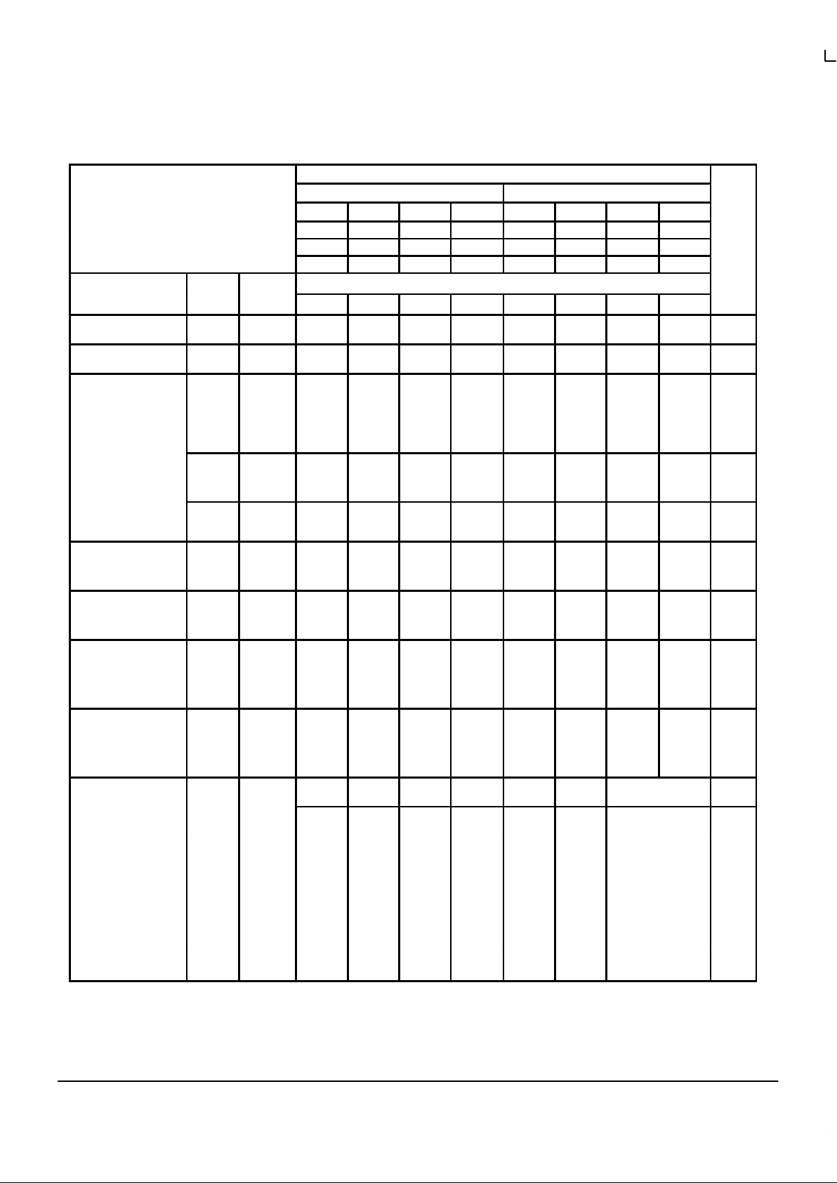
ELECTRICAL CHARACTERISTICS
TEST VOLTAGE VALUES (Volts)
MECL 10,000 INPUT LEVELS TTL INPUT LEVELS (6.)
@ Test Temperature V
IHmaxVILminVIHAminVILAmax
V
IH
V
IL
V
IHA′
V
ILA′
–30°C –0.890 –1.890 –1.155 –1.500 3.000 0.400 2.000 0.800
+25°C –0.810 –1.850 –1.105 –1.475 3.000 0.400 2.000 0.800
+85°C –0.700 –1.825 –1.035 –1.440 3.000 0.400 2.000 0.800
Pin
TEST VOLTAGE APPLIED TO PINS LISTED BELOW
Characteristic Symbol
Und
er
Test
V
IHmaxVILminVIHAminVILAmax
V
IH
V
IL
V
IHA′
V
ILA′
Gnd
Negative Power Supply
Drain Current
I
E
8
8
11
11
12
12
1,5,16
1,16
Positive Power Supply
Drain Current
I
CC
9 4,6,7,13 1,16
Input Current I
inH
4
6
7
10
11
12
13
10,11
11
12
4
6
7
13
1,16
1,16
1,16
1,16
1,16
1,16
1,16
I
CBO
(1.) 4
6
7
13
4
6
7
13
1,16
1,16
1,16
1,16
I
inL
10
11
12
10
11
12
1,16
1,16
1,16
Output Voltage
Logic 1
V
OH
2
3
2
3
12
12
12
12
10,11
10,11
10,11
10,11
4
6
4
6
1,16
1,16
1,5,16
1,5,16
Output Voltage
Logic 0
V
OL
2
3
2
3
12
12
12
12
10,11
10,11
10,11
10,11
4
6
4
6
1,16
1,16
1,5,16
1,5,16
Threshold Voltage
Logic 1
V
OHA
2 (2.)
2
2
2
2
(3.)
2 (4.)
11,12
10,12
12
12
12
10,11
10,11
10,11
10,11
12
10
11
4
4
4
4
1,16
1,16
1,16
1,16
1,5,16
1,5,16
Threshold Voltage
Logic 0
V
OLA
2 (2.)
2
2
(2.)
2
2
(3.)
2 (4.)
11,12
10,12
12
12
12
10,11
10,11
10,11
10,11
10
11
12
4
4
4
4
1,16
1,16
1,16
1,16
1,5,16
1,5,16
Switching Times
Propagation Delay
+1.11V +0.31V Pulse In
Pulse
Out
+5.0V +2.40V Figure +2.0V
Data Input t
7+14+
t
7–14–
14
14
12
12
10,11
10,11
7
7
14
14
Figure 3
Figure 3
1,16
1,16
Clock Input t
11–14+
t
11–14–
14
14
12
12
10
10
7,11
7,11
14
14
Figure 6
Figure 6
1,16
1,16
Strobe Input t
12+14+
t
12–14–
14
14
10,11
10,11
12
12
14
14
7
7
Figure 4
Figure 4
1,16
1,16
Reset Input t
10+14–
14 12 10,11 14 7 7 Figure 5 1,16
Hysteresis Mode t
7+14+
t
7–14–
14
14
12
12
10,11
10,11
7
7
14
14
Figure 3
Figure 3
1,5,16
1,5,16
Setup Time t
setup
14 12 10 7,1 1 14 Figure 7 1,16
Hold Time t
hold
14 12 10 7,11 14 Figure 7 1,16
Rise Time t+ 14 12 10,11 7 14 Figure 3 1,16
Fall Time t– 14 12 10,11 7 14 Figure 3 1,16
1. Pin 5 to VEE, VIL to Data input one at a time.
2. Output latched to logic high state prior to test. V
IHA
′, V
ILA
′ are standard logic 1 and logic 0 MTTL threshold voltages. V
IHA
′′, V
ILA
′′, V
IHA
′′′ and V
ILA
′′′ are logic 1 and
logic 0 threshold voltages in the hysteresis mode as shown in Figure 1 on page 3–2.
3. Input level on data input taken from +0.4V up to voltage level given.
4. Input level on data input taken from +4.0V down to voltage level given.
5. Operation and limits shown also apply for VCC = +6.0V. 6. When testing, choose either TTL or IBM input levels.
Page 4

MC10129
MOTOROLA MECL Data
DL122 — Rev 6
3–4
ELECTRICAL CHARACTERISTICS
TEST VOLTAGE VALUES (Volts)
IBM INPUT LEVELS (6.) HYSTERESIS MODE
@ Test Temperature V
IH
V
IL
V
IHA
′ V
ILA
′ V
IHA
′′ V
ILA
′′ V
IHA
′′′ V
ILA
′′′ V
CC
(5.) V
EE
–30°C 3.11 0.150 2.90 2.00 2.20 1.30 +5.0 –5.2
+25°C 3.11 0.150 1.700 0.70 2.60 1.70 1.90 1.00 +5.0 –5.2
+85°C 3.11 0.150 2.30 1.40 1.60 0.70 +5.0 –5.2
Pin
TEST VOLTAGE APPLIED TO PINS LISTED BELOW
Characteristic Symbol
Und
er
Test
V
IH
V
IL
V
IHA
′ V
ILA
′ V
IHA
′′ V
ILA
′′ V
IHA
′′′ V
ILA
′′′ V
CC
(5.) V
EE
Gnd
Negative Power Supply
Drain Current
I
E
8
8
9
9
8
5,8
1,5,16
1,16
Positive Power Supply
Drain Current
I
CC
9 4,6,
7,13
9
9
5,8
5,8
1,16
1,16
Input Current I
inH
4
6
7
10
11
12
13
4
6
7
13
9
9
9
9
9
9
9
8
8
8
8
8
8
8
1,16
1,16
1,16
1,16
1,16
1,16
1,16
I
CBO
(1.) 4
6
7
13
4
6
7
13
9
9
9
9
8
8
8
8
1,16
1,16
1,16
1,16
I
inL
10
11
12
9
9
9
8
8
8
1,16
1,16
1,16
Output Voltage
Logic 1
V
OH
2
3
2
3
4
6
4
6
9
9
9
9
5,8
5,8
8
8
1,16
1,16
1,5,16
1,5,16
Output Voltage
Logic 0
V
OL
2
3
2
3
4
6
4
6
9
9
9
9
5,8
5,8
8
8
1,16
1,16
1,5,16
1,5,16
Threshold Voltage
Logic 1
V
OHA
2 (2.)
2
2
2
2
(3.)
2 (4.)
4
4
4
4
4
4
9
9
9
9
9
9
5,8
5,8
5,8
5,8
8
8
1,16
1,16
1,16
1,16
1,5,16
1,5,16
Threshold Voltage
Logic 0
V
OLA
2 (2.)
2
2
(2.)
2
2
(3.)
2 (4.)
4
4
4
4
4
4
9
9
9
9
9
9
5,8
5,8
5,8
5,8
8
8
1,16
1,16
1,16
1,16
1,5,16
1,5,16
Switching Times
Propagation Delay
+5.0V +2.40V Figure +7.0V –3.2V +2.0V
Data Input t
7+14+
t
7–14–
14
14
Figure 3
Figure 3
9
9
5,8
5,8
1,16
1,16
Clock Input t
11–14+
t
11–14–
14
14
Figure 6
Figure 6
9
9
5,8
5,8
1,16
1,16
Strobe Input t
12+14+
t
12–14–
14
14
7
7
Figure 4
Figure 4
9
9
5,8
5,8
1,16
1,16
Reset Input t
10+14–
14 7 Figure 5 9 5,8 1,16
Hysteresis Mode t
7+14+
t
7–14–
14
14
Figure 3
Figure 3
9
9
881,5,16
1,5,16
Setup Time t
setup
14 Figure 7 9 5,8 1,16
Hold Time t
hold
14 Figure 7 9 5,8 1,16
Rise Time t+ 14 Figure 3 9 5,8 1,16
Fall Time t– 14 Figure 3 9 5,8 1,16
1. Pin 5 to VEE, VIL to Data input one at a time.
2. Output latched to logic high state prior to test. V
IHA
′, V
ILA
′ are standard logic 1 and logic 0 MTTL threshold voltages. V
IHA
′′, V
ILA
′′, V
IHA
′′′ and V
ILA
′′′ are logic 1 and
logic 0 threshold voltages in the hysteresis mode as shown in Figure 1 on page 3–2.
3. Input level on data input taken from +0.4V up to voltage level given.
4. Input level on data input taken from +4.0V down to voltage level given.
5. Operation and limits shown also apply for VCC = +6.0V. 6. When testing, choose either TTL or IBM input levels.
Page 5

MC10129
3–5 MOTOROLAMECL Data
DL122 — Rev 6
Q0
D0
D
C
R
Q1
D1
D
C
R
Q2
D2
D
C
R
Q3
D3
D
C
R
Hysteresis
Control 5
Clock 11
Reset 10
Strobe 12
V
out
Coax
1
8
25
µ
F
0.1
µ
F
+ 2.0 Vdc
–3.2 Vdc
V
EE
0.1 µF
Pulse Generator
Coax
V
in
Input
25 µF
+5.0 Vdc
V
CC
+7.0 Vdc
16
0.1 F
µ
4
6
13
7
2
3
15
14
Figure 2. SWITCHING TIME TEST CIRCUIT AND WAVEFORMS @ 25°C
50-ohm termination to ground located in each scope channel input.
All input and output cables to the
scope are equal lengths of 50-ohm
coaxial cable. Wire length should be
< 1/4 inch from TPin to input pin and
TP
out
to output pin.
Unused outputs
connected to a
50-ohm resistor
to ground.
Input Pulse
t+ = t– = 5.5
±
0.5 ns
(10 to 90%)
Unused Inputs (D)
must be tied to
VCC or Pin 16
NOTE: All power supplies and logic levels are shifted 2 volts positive.
Page 6

MC10129
MOTOROLA MECL Data
DL122 — Rev 6
3–6
Figure 3 – DATA to OUTPUT
(Clock and Reset are low, Strobe is high)
Figure 4 – STROBE to OUTPUT
(Data is high, Clock and Reset are low)
Figure 5 – RESET to OUTPUT
(Data and Strobe are high)
Figure 6 – CLOCK to OUTPUT
(Reset is low, Strobe is high)
Q
t
setup
50%
50%
t
hold
D
50%
+1.11 V
+0.31 V
+2.400 V
C
Figure 7 – T
SET UP
AND T
HOLD
WAVEFORMS
Q
+5.00 V
+5.0 V
Data
t
11–14–
50%50%
t–
80%
50%
20%
t+
t
11–14+
+1.11 V
Q
+0.31 V
+0.31 V
+1.11 V
+2.4 V
+1.11 V
t+
80%
50%
20%
t
10+14–
+1.11 V
t
11–14+
Reset
50%
Clock
+0.31 V
+0.31 V
+1.11 V
50%
Q
+0.31 V
t–
t+
t
12+14+
80%
50%
20%
Clock
Strobe
50%
+1.11 V
+0.31 V
t–
t
12–14–
+0.31 V
t+
80%
50%
20%
t
7–14–
t
7+14+
+0.31 V
+1.11 V
t–
+2.4 V
+5.0 V
Data
50%
Q
+1.11 V
Page 7

MC10129
3–7 MOTOROLAMECL Data
DL122 — Rev 6
OUTLINE DIMENSIONS
L SUFFIX
CERAMIC DIP PACKAGE
CASE 620–10
ISSUE V
NOTES:
1. DIMENSIONING AND TOLERANCING PER
ANSI Y14.5M, 1982.
2. CONTROLLING DIMENSION: INCH.
3. DIMENSION L TO CENTER OF LEAD WHEN
FORMED PARALLEL.
4. DIMENSION F MAY NARROW TO 0.76 (0.030)
WHERE THE LEAD ENTERS THE CERAMIC
BODY.
–A–
–B–
–T–
F
E
G
N
K
C
SEATING
PLANE
16 PLD
S
A
M
0.25 (0.010) T
16 PLJ
S
B
M
0.25 (0.010) T
M
L
DIM MIN MAX MIN MAX
MILLIMETERSINCHES
A 0.750 0.785 19.05 19.93
B 0.240 0.295 6.10 7.49
C ––– 0.200 ––– 5.08
D 0.015 0.020 0.39 0.50
E 0.050 BSC 1.27 BSC
F 0.055 0.065 1.40 1.65
G 0.100 BSC 2.54 BSC
H 0.008 0.015 0.21 0.38
K 0.125 0.170 3.18 4.31
L 0.300 BSC 7.62 BSC
M 0 15 0 15
N 0.020 0.040 0.51 1.01
____
16 9
18
Motorola reserves the right to make changes without further notice to any products herein. Motorola makes no warranty , representation or guarantee regarding
the suitability of its products for any particular purpose, nor does Motorola assume any liability arising out of the application or use of any product or circuit, and
specifically disclaims any and all liability, including without limitation consequential or incidental damages. “T ypical” parameters which may be provided in Motorola
data sheets and/or specifications can and do vary in different applications and actual performance may vary over time. All operating parameters, including “Typicals”
must be validated for each customer application by customer’s technical experts. Motorola does not convey any license under its patent rights nor the rights of
others. Motorola products are not designed, intended, or authorized for use as components in systems intended for surgical implant into the body, or other
applications intended to support or sustain life, or for any other application in which the failure of the Motorola product could create a situation where personal injury
or death may occur. Should Buyer purchase or use Motorola products for any such unintended or unauthorized application, Buyer shall indemnify and hold Motorola
and its officers, employees, subsidiaries, affiliates, and distributors harmless against all claims, costs, damages, and expenses, and reasonable attorney fees
arising out of, directly or indirectly, any claim of personal injury or death associated with such unintended or unauthorized use, even if such claim alleges that
Motorola was negligent regarding the design or manufacture of the part. Motorola and are registered trademarks of Motorola, Inc. Motorola, Inc. is an Equal
Opportunity/Affirmative Action Employer.
How to reach us:
USA/EUROPE/Locations Not Listed: Motorola Literature Distribution; JAPAN: Nippon Motorola Ltd.; Tatsumi–SPD–JLDC, 6F Seibu–Butsuryu–Center,
P.O. Box 5405, Denver, Colorado 80217. 303–675–2140 or 1–800–441–2447 3–14–2 Tatsumi Koto–Ku, Tokyo 135, Japan. 81–3–3521–8315
Mfax: RMFAX0@email.sps.mot.com – TOUCHT ONE 602–244–6609 ASIA/PACIFIC: Motorola Semiconductors H.K. Ltd.; 8B Tai Ping Industrial Park,
INTERNET: http://Design–NET.com 51 Ting Kok Road, Tai Po, N.T., Hong Kong. 852–26629298
MC10129/D
*MC10129/D*
◊
 Loading...