

Page 1
SEMICONDUCTOR TECHNICAL DATA
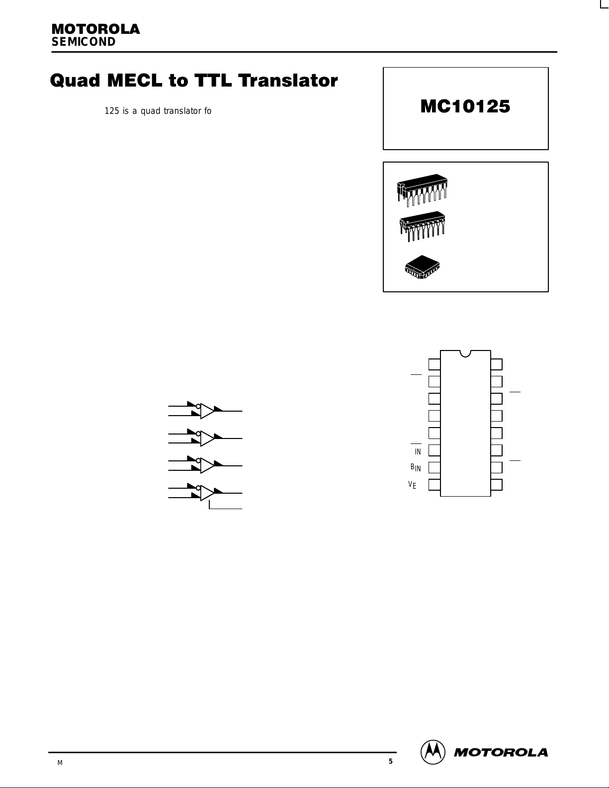
The MC10125 is a quad translator for interfacing data and control signals
between the MECL section and saturated logic sections of digital systems. The
MC10125 incorporates differential inputs and Schottky TTL “totem pole”
outputs. Differential inputs allow for use as an inverting/ non–inverting translator
or as a differential line receiver . The VBB reference voltage is available on pin 1
for use in single–ended input biasing. The outputs of the MC10125 go to a low
logic level whenever the inputs are left floating.
Power supply requirements are ground, +5.0 Volts and –5.2 Volts.
Propagation delay of the MC10125 is typically 4.5 ns. The MC10125 has fanout
of 10 TTL loads. The dc levels are MECL 10,000 in and Schottky TTL, or TTL
out. This device has an input common mode noise rejection of
± 1.0 Volt.
An advantage of this device is that MECL level information can be received,
via balanced twisted pair lines, in the TTL equipment. This isolates the MECL
logic from the noisy TTL environment. This device is useful in computers,
instrumentation, peripheral controllers, test equipment and digital
communications systems.
PD= 380 mW typ/pkg (No Load)
tpd= 4.5 ns typ (50% to + 1.5 Vdc out)
tr, tf= 2.5 ns typ (1.0 V to 2.0 V)
LOGIC DIAGRAM
2
3
6
7
10
11
14
15
VBB*
Gnd = PIN 16
VCC (+5.0Vdc) = PIN 9
VEE (–5.2Vdc) = PIN 8
4
5
12
13
1
L SUFFIX
CERAMIC PACKAGE
CASE 620–10
P SUFFIX
PLASTIC PACKAGE
CASE 648–08
FN SUFFIX
PLCC
CASE 775–02
DIP
PIN ASSIGNMENT
V
BB
A
IN
A
IN
A
OUT
B
OUT
B
IN
B
IN
V
EE
Pin assignment is for Dual–in–Line Package.
For PLCC pin assignment, see the Pin Conversion
T ables on page 6–11 of the Motorola MECL Data
1
2
3
4
5
6
7
8
Book (DL122/D).
16
15
14
13
12
11
10
GND
D
IN
D
IN
D
OUT
C
OUT
C
IN
C
IN
V
9
CC
*VBB to be used to supply bias to the MC10125 only and bypassed (when used)
with 0.01 µF to 0.1 µF capacitor to ground (0 V). VBB can source < 1.0 mA.
When the input pin with the bubble goes positive, the output goes negative.
3/93
Motorola, Inc. 1996
3–89
REV 5
Page 2
MC10125
Under
pp y
p
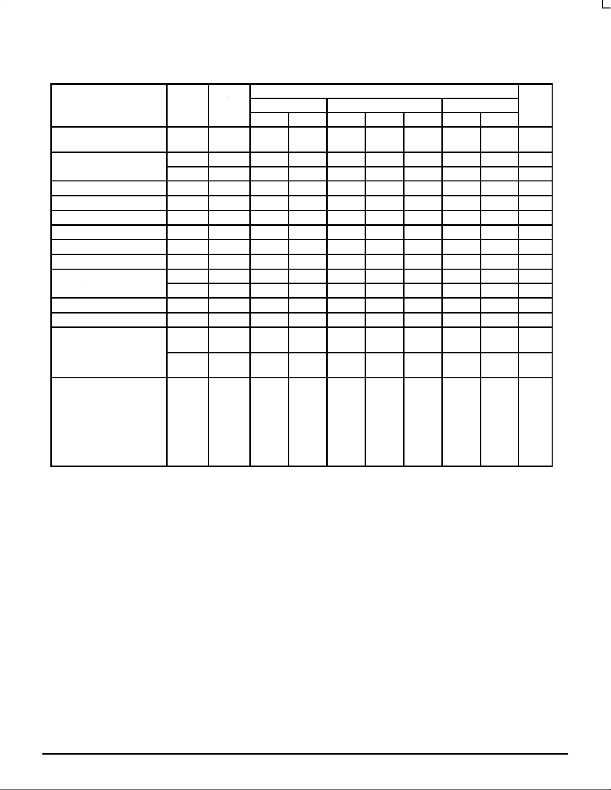
ELECTRICAL CHARACTERISTICS
Test Limits
Pin
Characteristic Symbol
Negative Power Supply Drain
Current
Positive Power Supply Drain
Current
Input Current I
Input Leakage Current I
High Output Voltage V
Low Output Voltage V
High Threshold Voltage V
Low Threshold Voltage V
Indeterminate Input
Protection Tests
Short Circuit Current I
Reference Voltage V
Common Mode Rejection
Tests
Switching Times (50Ω Load) ns
Propagation Delay
(50% to +1.5Vdc)
Rise Time (+1.0V to 2.0V) t
Fall Time (+1.0V to 2.0V) t
1. Individually test each output, apply V
I
CCH
I
CCL
inH
CBO
OHA
V
OLS1
V
OLS2
V
V
t
6+5–
t
6–5+
t
2+4–
t
2–4+
I
E
OH
OL
OLA
OS
BB
OH
OL
4+
4–
Under
Test
1
to pin under test.
IHmax
8 –44 –40 –44 mAdc
9 52 52 52 mAdc
9 39 39 39 mAdc
2 180 115 115 µAdc
2 1.5 1.0 1.0 µAdc
4 2.5 2.5 2.5 Vdc
4 0.5 0.5 0.5 Vdc
4 2.5 2.5 2.5 Vdc
4 0.5 0.5 0.5 Vdc
4 0.5 0.5 0.5 Vdc
4 0.5 0.5 0.5 Vdc
4 40 100 40 100 40 100 mAdc
1 –1.420 –1.280 –1.350 –1.230 –1.295 –1.150 Vdc
4
4
4
4
5
5
4
4
4 3.3 3.3 3.3
4 3.3 3.3 3.3
–30°C +25°C +85°C
Min Max Min Typ Max Min Max
2.5
2.5
1.0
1.0
1.0
1.0
0.5
0.5
6.0
6.0
6.0
6.0
2.5
2.5
1.0
1.0
1.0
1.0
4.5
4.5
4.5
4.5
0.5
0.5
6.0
6.0
6.0
6.0
2.5
2.5
1.0
1.0
1.0
1.0
0.5
0.5
6.0
6.0
6.0
6.0
Unit
Vdc
Vdc
MOTOROLA MECL Data
3–90
DL122 — Rev 6
Page 3
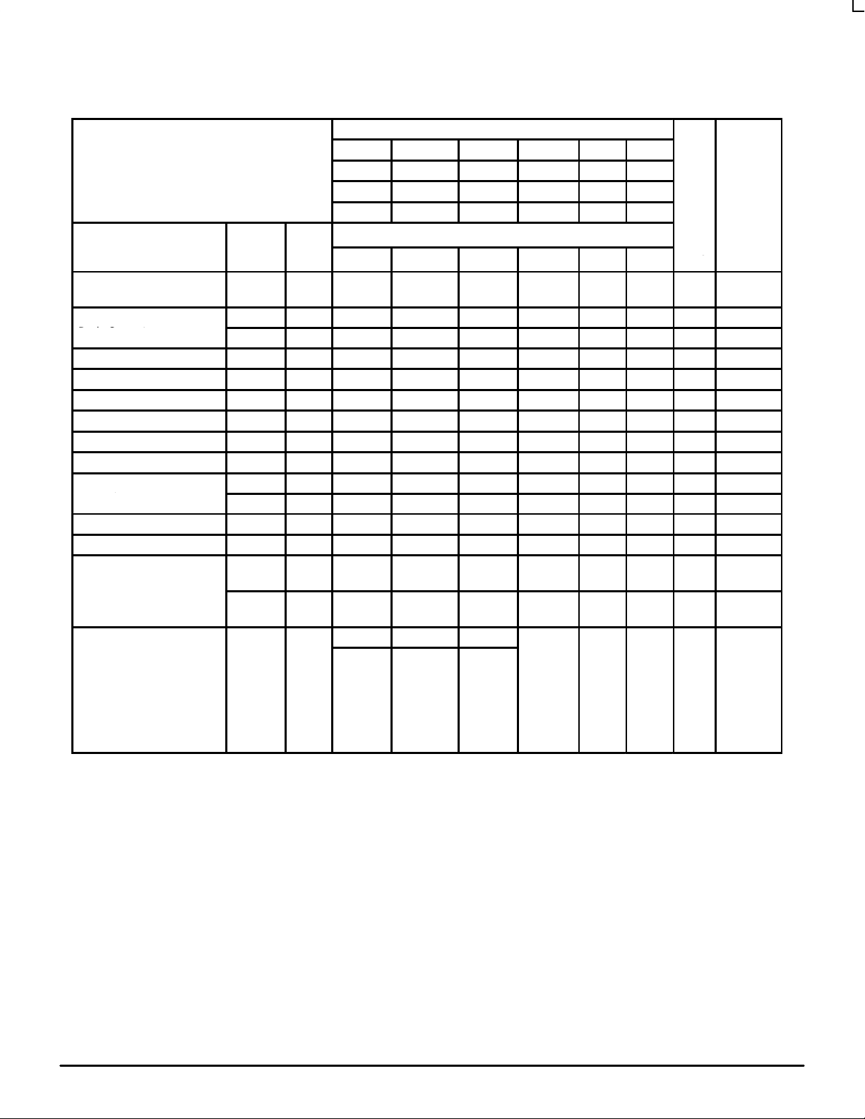
ELECTRICAL CHARACTERISTICS (continued)
Und
pp y
p
TEST VOLTAGE VALUES (Volts)
@ Test Temperature V
–30°C –0.890 –1.890 –1.205 –1.500 +0.110 –0.890
+25°C –0.810 –1.850 –1.105 –1.475 +0.190 –0.850
+85°C –0.700 –1.825 –1.035 –1.440 +0.300 –0.825
Pin
Characteristic Symbol
Negative Power Supply
Drain Current
Positive Power Supply
Drain Current
Input Current I
Input Leakage Current I
High Output Voltage V
Low Output Voltage V
High Threshold Voltage V
Low Threshold Voltage V
Indeterminate Input
Protection Tests
Short Circuit Current I
Reference Voltage V
Common Mode Rejection
Tests
Switching Times(50Ω Load) Pulse In Pulse Out CL (pF)
Propagation Delay
(50% to +1.5Vdc)
Rise Time (+1.0V to 2.0V) t
Fall Time (+1.0V to 2.0V) t
1. Individually test each output, apply V
I
CCH
I
CCL
inH
CBO
V
OLS1
V
OLS2
V
V
t
6+5–
t
6–5+
t
2+4–
t
2–4+
I
E
OH
OL
OHA
OLA
OS
BB
OH
OL
4+
4–
1
IHmax
Test
8 16
9 2,6,10,14 16
9 2,6,10,14
2 2,6,10,14 16
2 16
4 2,6,10,14 16 –2.0mA
4 2,6,10,14 16 20mA
4 6,10,14 2 16 –2.0mA
4 6,10,14 2 16 20mA
4 16 20mA
4 16 20mA
4 2,6,10,14 4, 16
1 2,6,10,14
4
4
4
4
5
5
4
4
4 2 4 25 16
4 2 4 25 16
to pin under test.
IHmax
er
V
IHmax
6
6
2
2
V
ILmin
TEST VOLTAGE APPLIED TO PINS LISTED BELOW
V
ILmin
5
5
4
4
V
IHAminVILAmaxVIHH
V
IHAminVILAmaxVIHH
25
25
25
25
V
ILH
ILH
Gnd
V
3 2 16
2 3 16
MC10125
Condition
16
16
16
16
16
16
16
Output
–2.0mA
–2.0mA
20mA
20mA
DL122 — Rev 6
3–91 MOTOROLAMECL Data
Page 4

MC10125
From
Und
pp y
ELECTRICAL CHARACTERISTICS (continued)
TEST VOLTAGE VALUES (Volts)
@ Test Temperature V
–30°C –1.890 –2.890
+25°C –1.810 –2.850
+85°C –1.700 –2.825
Pin
Characteristic Symbol
Negative Power Supply
Drain Current
Positive Power Supply
Drain Current
Input Current I
Input Leakage Current I
High Output Voltage V
Low Output Voltage V
High Threshold Voltage V
Low Threshold Voltage V
Indeterminate Input
Protection Tests
Short Circuit Current I
Reference Voltage V
Common Mode Rejection Tests V
Switching Times (50Ω Load)
Propagation Delay
(50% to +1.5Vdc)
Rise Time (+1.0V to 2.0V) t
Fall Time (+1.0V to 2.0V) t
1. Individually test each output, apply V
Each MECL 10,000 series circuit has been designed to meet the dc specifications shown in the test table, after thermal equilibrium has been
established. The circuit is in a test socket or mounted on a printed circuit board and transverse air flow greater than 500 linear fpm is maintained.
Outputs are terminated through a 50-ohm resistor to –2.0 volts. Test procedures are shown for only one gate. The other gates are tested in the
same manner.
I
E
I
CCH
I
CCL
1
inH
CBO
OH
OL
OHA
OLA
V
OLS1
V
OLS2
OS
BB
OH
V
OL
t
6+5–
t
6–5+
t
2+4–
t
2–4+
4+
4–
to pin under test.
IHmax
er
Test
V
8 3,7,1 1,15 9 8 16
9 3,7,1 1,15 9 8 16
9 3,7,1 1,15 9 8
2 3,7,11,15 9 8 16
2 3,7,1 1,15 9 2,6,8,10,14 16
4 3,7,1 1,15 9 8 16 –2.0mA
4 3,7,1 1,15 9 8 16 20mA
4 3,7,1 1,15 9 8 16 –2.0mA
4 3,7,11,15 9 8 16 20mA
4 9 2,3,6,7,8,
4 9 8 16 20mA
4 3,7,1 1,15 9 8 4, 16
1 3,7,11,15
4
4
4
4
5
5
4
4
4 3,7,11,15 9 8 16
4 3,7,11,15 9 8 16
V
IHH
TEST VOLTAGE APPLIED TO PINS LISTED BELOW
IHH
3 2
2 3
ILH
V
ILH
V
BB
From
Pin
1
V
BB
3,7,1 1,15
3,7,1 1,15
3,7,1 1,15
3,7,1 1,15
V
CC
+5.0 –5.2
+5.0 –5.2
+5.0 –5.2
V
CC
9
9
9
9
9
9
9
9
V
EE
V
EE
10,11,14,15
8
8
8
8
8
8
8
8
Gnd
Output
Condition
16
16 20mA
1616–2.0mA
–2.0mA
16
16
16
16
16
16
20mA
20mA
MOTOROLA MECL Data
3–92
DL122 — Rev 6
Page 5

SWITCHING TIME TEST CIRCUIT
MC10125
V
in
Coax
Input
Pulse Generator
Input Pulse
±
t+ = t– = 2.0
(20 to 80%)
50-ohm termination to ground located
in each scope channel input.
All input and output cables to the
scope are equal lengths of 50-ohm
coaxial cable. Wire length should be
< 1/4 inch from TPin to input pin and
TP
to output pin.
out
0.2 ns
–1.69 Vdc
0.1 µF
2
3
6
7
10
11
14
15
1
16 8
V
CC
V
BB
+5.0 Vdc
0.1 µF
–5.2 Vdc
V
EE
4
5
12
13
0.1
V
out
Coax
450
C
L
CL = 25 pF, including test fixture
One input from each gate must be tied to V
(Pin 1) during testing.
µ
F
BB
DL122 — Rev 6
3–93 MOTOROLAMECL Data
Page 6

MC10125
OUTLINE DIMENSIONS
FN SUFFIX
PLASTIC PLCC PACKAGE
CASE 775–02
ISSUE C
–L–
20 1
Z
C
G
G1
0.010 (0.250) N
S
T
–N–
L–M
S
Y BRK
–M–
W
V
A
0.007 (0.180) N
0.007 (0.180) N
R
E
0.004 (0.100)
J
PLANE
SEATING
–T–
VIEW S
S
0.007 (0.180) N
B
0.007 (0.180) N
U
M
S
L–M
T
M
S
S
L–M
T
S
D
Z
D
X
0.010 (0.250) N
G1
S
S
L–M
T
S
VIEW D–D
M
M
S
L–M
T
L–M
T
S
S
S
0.007 (0.180) N
H
M
S
L–M
T
S
K1
K
0.007 (0.180) N
F
M
S
L–M
T
S
VIEW S
NOTES:
1. DATUMS –L–, –M–, AND –N– DETERMINED
WHERE TOP OF LEAD SHOULDER EXITS PLASTIC
BODY AT MOLD PARTING LINE.
2. DIMENSION G1, TRUE POSITION TO BE
MEASURED AT DA TUM –T–, SEATING PLANE.
3. DIMENSIONS R AND U DO NOT INCLUDE MOLD
FLASH. ALLOWABLE MOLD FLASH IS 0.010 (0.250)
PER SIDE.
4. DIMENSIONING AND TOLERANCING PER ANSI
Y14.5M, 1982.
5. CONTROLLING DIMENSION: INCH.
6. THE PACKAGE TOP MAY BE SMALLER THAN THE
PACKAGE BOTTOM BY UP TO 0.012 (0.300).
DIMENSIONS R AND U ARE DETERMINED AT THE
OUTERMOST EXTREMES OF THE PLASTIC BODY
EXCLUSIVE OF MOLD FLASH, TIE BAR BURRS,
GATE BURRS AND INTERLEAD FLASH, BUT
INCLUDING ANY MISMATCH BETWEEN THE TOP
AND BOTTOM OF THE PLASTIC BODY.
7. DIMENSION H DOES NOT INCLUDE DAMBAR
PROTRUSION OR INTRUSION. THE DAMBAR
PROTRUSION(S) SHALL NOT CAUSE THE H
DIMENSION TO BE GREATER THAN 0.037 (0.940).
THE DAMBAR INTRUSION(S) SHALL NOT CAUSE
THE H DIMENSION TO BE SMALLER THAN 0.025
(0.635).
MOTOROLA MECL Data
DIM MIN MAX MIN MAX
A 0.385 0.395 9.78 10.03
B 0.385 0.395 9.78 10.03
C 0.165 0.180 4.20 4.57
E 0.090 0.1 10 2.29 2.79
F 0.013 0.019 0.33 0.48
G 0.050 BSC 1.27 BSC
H 0.026 0.032 0.66 0.81
J 0.020 ––– 0.51 –––
K 0.025 ––– 0.64 –––
R 0.350 0.356 8.89 9.04
U 0.350 0.356 8.89 9.04
V 0.042 0.048 1.07 1.21
W 0.042 0.048 1.07 1.21
X 0.042 0.056 1.07 1.42
Y ––– 0.020 ––– 0.50
Z 2 10 2 10
____
G1 0.310 0.330 7.88 8.38
K1 0.040 ––– 1.02 –––
3–94
MILLIMETERSINCHES
DL122 — Rev 6
Page 7

OUTLINE DIMENSIONS
CERAMIC DIP PACKAGE
–A–
16 9
–B–
18
C
–T–
SEATING
PLANE
N
E
F
G
16 PLD
0.25 (0.010) T
M
–A–
916
B
18
F
C
S
H
G
D
16 PL
0.25 (0.010) T
K
M
K
S
A
PLASTIC DIP PACKAGE
SEATING
–T–
PLANE
M
A
L SUFFIX
CASE 620–10
ISSUE V
L
M
16 PLJ
0.25 (0.010) T
P SUFFIX
CASE 648–08
ISSUE R
L
J
MC10125
NOTES:
1. DIMENSIONING AND TOLERANCING PER
ANSI Y14.5M, 1982.
2. CONTROLLING DIMENSION: INCH.
3. DIMENSION L TO CENTER OF LEAD WHEN
FORMED PARALLEL.
4. DIMENSION F MAY NARROW TO 0.76 (0.030)
WHERE THE LEAD ENTERS THE CERAMIC
BODY.
DIM MIN MAX MIN MAX
A 0.750 0.785 19.05 19.93
B 0.240 0.295 6.10 7.49
C ––– 0.200 ––– 5.08
D 0.015 0.020 0.39 0.50
E 0.050 BSC 1.27 BSC
F 0.055 0.065 1.40 1.65
G 0.100 BSC 2.54 BSC
H 0.008 0.015 0.21 0.38
K 0.125 0.170 3.18 4.31
M
S
B
NOTES:
1. DIMENSIONING AND TOLERANCING PER ANSI
2. CONTROLLING DIMENSION: INCH.
3. DIMENSION L TO CENTER OF LEADS WHEN
4. DIMENSION B DOES NOT INCLUDE MOLD FLASH.
5. ROUNDED CORNERS OPTIONAL.
M
L 0.300 BSC 7.62 BSC
M 0 15 0 15
____
N 0.020 0.040 0.51 1.01
Y14.5M, 1982.
FORMED PARALLEL.
DIM MIN MAX MIN MAX
A 0.740 0.770 18.80 19.55
B 0.250 0.270 6.35 6.85
C 0.145 0.175 3.69 4.44
D 0.015 0.021 0.39 0.53
F 0.040 0.70 1.02 1.77
G 0.100 BSC 2.54 BSC
H 0.050 BSC 1.27 BSC
J 0.008 0.015 0.21 0.38
K 0.110 0.130 2.80 3.30
L 0.295 0.305 7.50 7.74
M 0 10 0 10
S 0.020 0.040 0.51 1.01
MILLIMETERSINCHES
MILLIMETERSINCHES
____
Motorola reserves the right to make changes without further notice to any products herein. Motorola makes no warranty , representation or guarantee regarding
the suitability of its products for any particular purpose, nor does Motorola assume any liability arising out of the application or use of any product or circuit, and
specifically disclaims any and all liability, including without limitation consequential or incidental damages. “T ypical” parameters which may be provided in Motorola
data sheets and/or specifications can and do vary in different applications and actual performance may vary over time. All operating parameters, including “Typicals”
must be validated for each customer application by customer’s technical experts. Motorola does not convey any license under its patent rights nor the rights of
others. Motorola products are not designed, intended, or authorized for use as components in systems intended for surgical implant into the body, or other
applications intended to support or sustain life, or for any other application in which the failure of the Motorola product could create a situation where personal injury
or death may occur. Should Buyer purchase or use Motorola products for any such unintended or unauthorized application, Buyer shall indemnify and hold Motorola
and its officers, employees, subsidiaries, affiliates, and distributors harmless against all claims, costs, damages, and expenses, and reasonable attorney fees
arising out of, directly or indirectly, any claim of personal injury or death associated with such unintended or unauthorized use, even if such claim alleges that
Motorola was negligent regarding the design or manufacture of the part. Motorola and are registered trademarks of Motorola, Inc. Motorola, Inc. is an Equal
Opportunity/Affirmative Action Employer.
How to reach us:
USA/EUROPE/Locations Not Listed: Motorola Literature Distribution; JAPAN: Nippon Motorola Ltd.; Tatsumi–SPD–JLDC, 6F Seibu–Butsuryu–Center,
P.O. Box 20912; Phoenix, Arizona 85036. 1–800–441–2447 or 602–303–5454 3–14–2 Tatsumi Koto–Ku, Tokyo 135, Japan. 03–81–3521–8315
MFAX: RMF AX0@email.sps.mot.com – T OUCHTONE 602–244–6609 ASIA/ PACIFIC: Motorola Semiconductors H.K. Ltd.; 8B Tai Ping Industrial Park,
INTERNET: http://Design–NET .com 51 Ting Kok Road, Tai Po, N.T., Hong Kong. 852–26629298
MC10125/D
DL122 — Rev 6
◊
3–95 MOTOROLAMECL Data
*MC10125/D*
 Loading...