

Page 1
Order this document
from Logic Marketing
MOTOROLA
SEMICONDUCTOR TECHNICAL DATA
Motorola, Inc. 1994
4/94
REV 0
Advance Information
CMI Coder/Decoder
The MC100SX1230 device consists of a Binary to CMI Coder and CMI
to Binary Decoder with integrated loop back capability. The device is
designed for CMI (Code Mark Inversion) interfaces in transmission
applications supporting either 139.26 Mbit/s E4 or 155.52 Mbit/s STM1
line rates.
• Binary-to-CMI Coder and CMI-to-Binary Decoder
• Internal Loop Back Test Capability
• Supports SDH or PDH Applications
• Low Power
• Fully Differential 100K Compatible I/O
• V
BB
Reference Available
• 75kΩ Input Pulldown Resistors
• +5V PECL or –5V ECL Operation
• 28-Pin Surface Mount PLCC Package
• Asynchronous Reset
In normal operation, the coder and decoder operate independently.
Both the coder and decoder operate from a 2X line rate clock. The device
incorporates test circuitry to support loop back bypass so either the coder
input can be routed to the decoder output or the decoder input can be
routed to the coder output. The part is fabricated using Motorola’s proven
MOSAIC III advanced bipolar process.
The device provides a VBB output for accepting single-ended inputs.
The VBB pin should only be used as a bias for the
MC100SX1230 as its
current sink/source capability is limited. Whenever used, the VBB pin
should be bypassed to ground via a 0.01µF capacitor.
1
DCLK
out
V
CC
V
CC
V
CCO
V
CCO
N/C
N/C
RESET
V
BB
DCLK
in
DCLK
in
V
EE
V
EE
LBIN
LCMI
4
3
2
28
27
26
25
24
23
22
21
20
19
18
17
16
15
14
13
12
11109
7
8
6
5
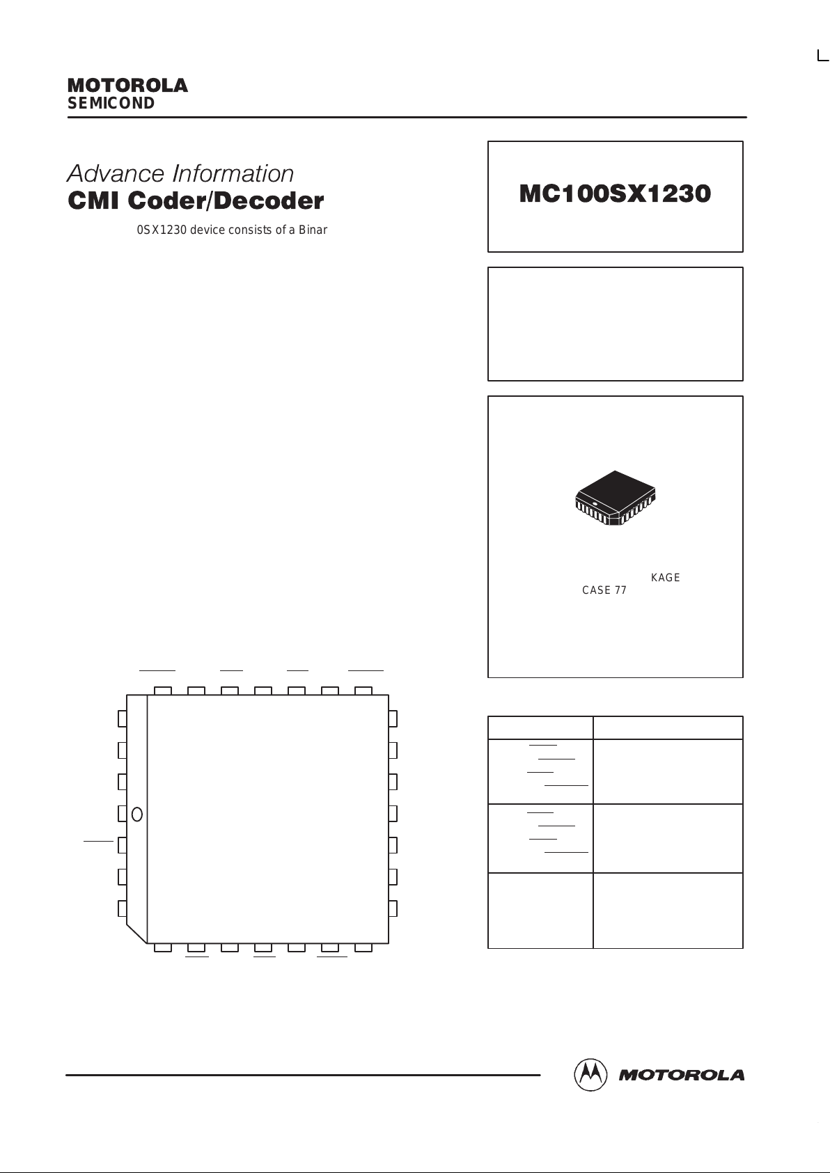
Pinout: 28-Lead PLCC
(Top View)
CMI
in
CCLK
out
CMI
in
QCMI
BIN
in
QCMI
BIN
in
QBIN
CCLK
in
QBIN
CCLK
in
DCLK
out
CCLK
out
MOSAIC III is a trademark of Motorola, Inc.
This document contains information on a new product. Specifications and information herein are subject to
change without notice.
MC100SX1230
CMI CODER/DECODER
FN SUFFIX
PLASTIC PLCC PACKAGE
CASE 776-02
PIN NAMES
Function
CMI Input to Decoder
Decoder Clock Input
Binary Output From Decoder
Decoder Clock Output
Binary Input to Coder
Coder Clock Input
CMI Output from Coder
Coder Clock Output
Asynchronous Reset
Control Input for Binary
Loop Back
Control Input for CMI
Loop Back
Pins
CMIin, CMI
in
DCLKin, DCLK
in
QBIN, QBIN
DCLK
out
, DCLK
out
BINin, BIN
in
CCLKin, CCLK
in
QCMI, QCMI
CCLK
out
, CCLK
out
RESET
LBIN
LCMI
Page 2
MC100SX1230
2
MOTOROLA High Performance Frequency
Control Products — BR1334
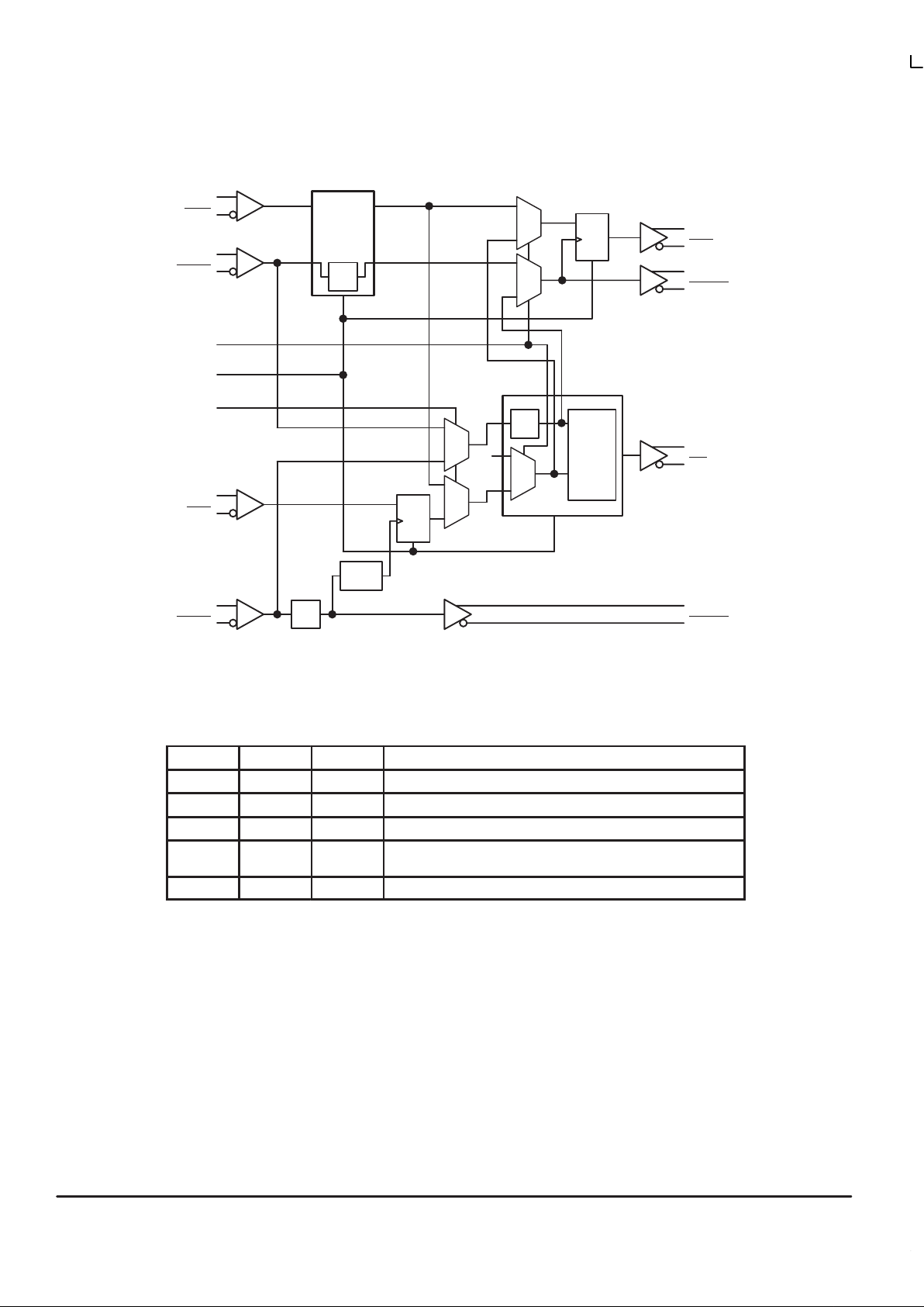
BLOCK DIAGRAM
CMI
in
CMI
in
DCLK
in
DCLK
in
DECODER
÷2
LBIN
QBIN
QBIN
DCLK
out
DCLK
out
D
C
R
CODER
÷2
R
CMI
CMI
H
LCMI
D
C
R
BIN
in
BIN
in
RESET
DELAY
CCLK
in
CCLK
in
÷2
CCLK
out
CCLK
out
FUNCTION TABLE
RESET LBIN LCMI
Function
H X X Reset, All Output Pairs Set to Logic Low State
L L L Independent Coder and Decoder Operation
L L H CMI Input Routed to Coder Output
L H L Binary Input and Clock Routed to Decoder Outputs
Alarm Indication Signal Output from Coder
L H H Illegal, Undefined Operation
Page 3
MC100SX1230
3
MOTOROLAHigh Performance Frequency
Control Products — BR1334
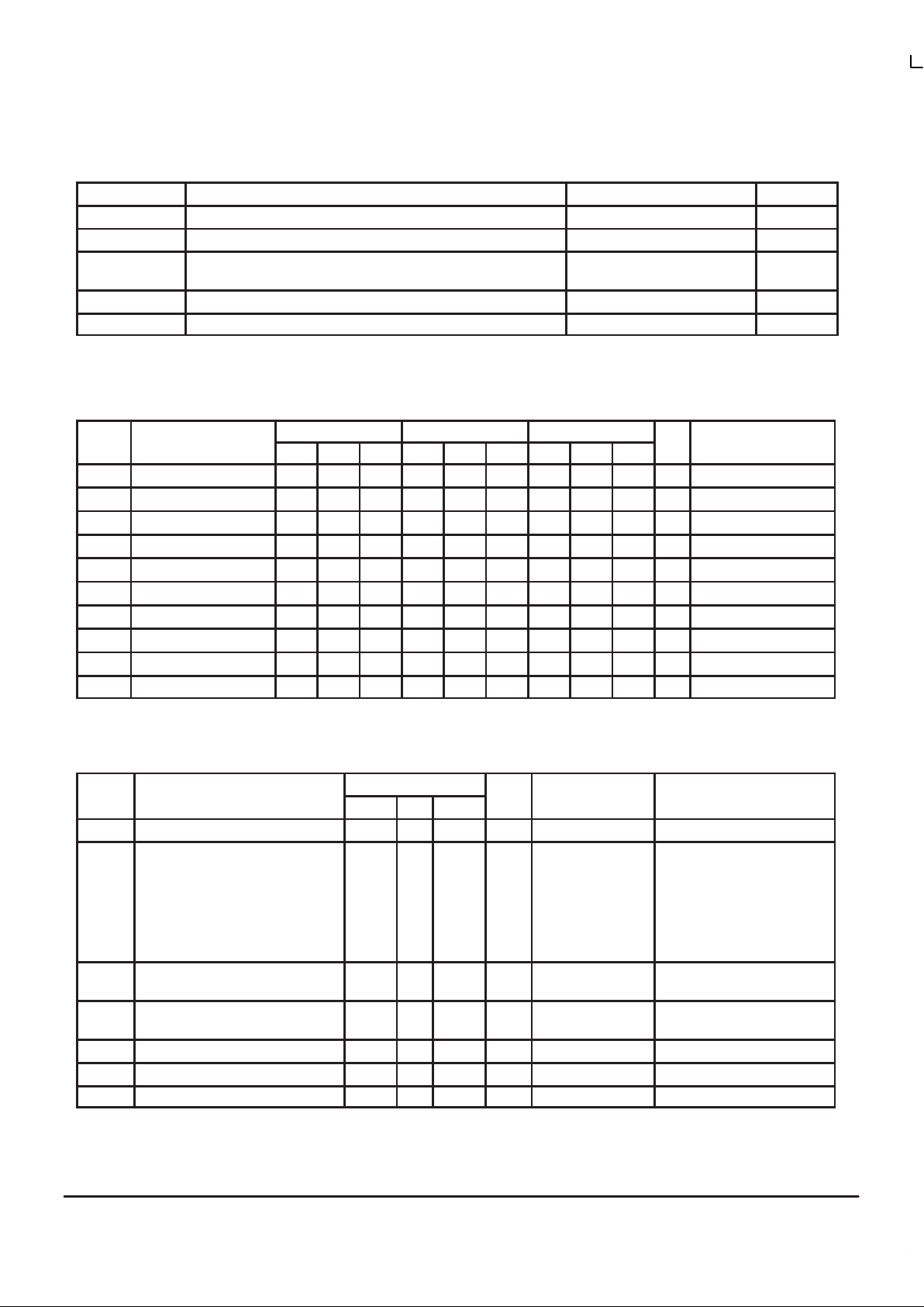
ABSOLUTE MAXIMUM RATINGS
1
Symbol Parameter Value Unit
V
EE
Power Supply (VCC = 0V) –8 to 0 Vdc
V
I
Input Voltage (VCC = 0V) 0 to –6 Vdc
I
OUT
Output Current Continuous
Surge
50
100
mA
T
A
Operating Temperature Range 0 to +85 °C
V
EE
Operating Range
2
–5.7 to 4.2 V
1 Absolute Maximum Ratings are those values beyond which damage to the device may occur. Functional operation should be restricted to the
Recommended Operating Conditions.
2 Parametric values specified at: –4.2 to 5.46V
DC CHARACTERISTICS (VCC = V
CCO
= GND; VEE = –4.2 to 5.46V)
0°C 25°C 85°C
Symbol Characteristic Min Typ Max Min Typ Max Min Typ Max Unit Condition
V
OH
Output HIGH Voltage –1025 –955 –880 –1025 –955 –880 –1025 –955 –880 mV Vin = V
IH(max)
or V
IL(min)
V
OL
Output LOW Voltage –1810 –1705 –1620 –1810 –1705 –1620 –1810 –1705 –1620 mV Vin = V
IH(max)
or V
IL(min)
V
OHA
Output HIGH Voltage –1035 –1035 –1035 mV Vin = V
IH(max)
or V
IL(min)
V
OLA
Output LOW Voltage –1610 –1610 –1610 mV Vin = V
IH(max)
or V
IL(min)
V
IH
Input HIGH Voltage –1165 –880 –1165 –880 –1165 –880 mV
V
IL
Input LOW Voltage –1810 –1475 –1810 –1475 –1810 –1475 mV
V
BB
Reference Voltage –1380 –1260 –1380 –1260 –1380 –1260 V
I
IH
Input HIGH Current 200 200 200 µA
I
IL
Input LOW Current 0.5 0.5 0.5 µA
I
EE
Supply Current 61 122 61 122 70 141 mA
1. 100SX circuits are designed to meet the DC specifications shown in the table after thermal equilibrium has been established. The circuit is mounted in a test socket
or mounted on a printed circuit board and transverse air greater than 500lfm is maintained.
2. All outputs are loaded with 50Ω to VCC – 2V.
AC CHARACTERISTICS (VCC = V
CCO
= GND; VEE = –4.2 to 5.46V)
0 to 85°C
Symbol Characteristic Min Typ Max Unit Condition Notes
F
max
700 MHz
t
pd
Propagation CCLKin to CCLK
out
Delay CCLKin to QCMI
DCLKin to DCLK
out
DCLKin to QBIN
CCLKin to DCLK
out
CCLKin to QBIN
DCLKin to QCMI
650
1000
550
1000
1100
800
1550
1750
1700
1800
2700
1700
ps
LCMI=LBIN=‘L’
LCMI=LBIN=‘L’
LCMI=LBIN=‘L’
LCMI=‘L’, LBIN=‘H’
LCMI=‘L’, LBIN=‘L’
LCMI=‘H’, LBIN=‘L’
Add 3 CCLKin-Cycles to Delay
Add 4 DCLKin-Cycles to Delay
Add 3 CCLKin-Cycles to Delay
Add 5 DCLKin-Cycles to Delay
t
s
Setup Time BINin to CCLK
in
CMIin to DCLK
in
–375
140
ps
t
h
Hold Time CCLKin to BIN
in
DCLKin to CMI
in
1000
120
ps
V
PP
Minimum Input Swing 250 mV
V
CMR
Common Mode Range –0.4 Note V
tr, t
f
Rise/Fall Times 150 700 ps 20% – 80%
1. 100SX circuits are designed to meet the AC specifications shown in the table after thermal equilibrium has been established. The circuit is mounted in a test socket
or mounted on a printed circuit board and transverse air greater than 500lfm is maintained.
2. The CMR range is referenced to the most positive side of the differential input signal. Normal operation is obtained if the HIGH level falls within the specified range
and the peak-to-peak voltage lies between VPPmin and 1V. The lower end of the CMR range is dependent on VEE and is equal to VEE + 3.0V.
Page 4

MC100SX1230
4
MOTOROLA High Performance Frequency
Control Products — BR1334
Applications Information
CMI Code
The CMI code is a 1B2B code. Each information bit is
coded into two transmission bits. A binary 0 is coded to 01,
and a binary 1 is coded alternately to a 00 or a 11, thus there
is at least one transition during every bit period. A typical
data pattern is illustrated in the figure below. Because of the
coding, the data stream is not only DC balanced, but it
contains a rich clock component which aids the clock
recovery process at the receiver. A 2X clock is used by the
MC100SX1230 to ensure that the mid-bit transition of the
data 0 is ideally centered at the CMI encoded output.
Figure 1. CMI Code
Binary
CMI
00110
00110
Typical Application
In a traditional telecommunications application, the
MC100SX1230 is resident on the line card interface which
contains circuitry to implement the line transmitter and
receiver functions. On the decoder side, a cable equalization
filter followed by a clock recovery/decision circuit are
required to compensate for the cable attenuation and
distortion, extract the 2X clock signal and re-time the CMI
data. On the coder side, a PLL is required to synthesize the
2X coder clock and a conditioning circuit is needed at the
output of the coder to generate the appropriate signal to drive
the cable.
Device Operation
The circuit contains a complete CMI coder and decoder as
well as the support circuitry necessary to perform loop back
of either the Binary input or the CMI input. The operation is
controlled by the LCMI and LBIN inputs. In addition, the
device generates an AIS (Alarm Indication Signal) from the
coder output when the binary loop back state is active
(LBIN=‘H’). The AIS signal indicates to the receiver at the
other end of the cable that ‘real’ data is not being sent. The
device contains a Reset input which should normally be reset
as part of the powering up sequence.
The coder accepts a differential data input (BINin) as well
as a differential clock (CCLKin). The clock signal must be
twice the frequency of the input data signal, i.e. a 155 MBit/s
binary signal requires a 310 MHz clock, for proper operation.
Typical input and output waveforms are shown in Figure 2.
The incoming clock signal is divided by 2 and supplied at the
coder clock output (CLK
out
). The BINin signal is buffered
before being driven into the input register which clocks in the
binary data. This results in a negative setup time for the
coder. The coded data is output from the coder 3 CCLK
in
clock cycles plus normal propagation delay after the binary
data has been supplied.
The decoder accepts a differential data input (CMIin) as
well as a differential clock (DCLKin). The clock signal is
supplied from the external clock extraction circuit and runs at
the coded rate of either 280 MHz or 310 MHz depending on
weather the application is for a PDH system or an SDH
system. The decoder has a latency of 4 clock cycles so the
decoded data is output 4 cycles plus the normal propagation
delay after the input data is captured. Figure 3 illustrates the
decoder operation.
Under certain conditions, the user may require that the
binary data to be coded be routed back to the output of the
decoder to verify proper system operation. This is accomplished through the use of the LBIN input control pin. When
this signal is asserted (LBIN = ‘H’), the BINin signal as well
as a divided by 2 version of the CCLKin input is routed to the
QBIN and DCLK
out
outputs respectively. The BINin to QBIN
output has a latency of 3 CCLKin cycles plus internal
propagation delays. In addition, the AIS signal is generated
and output from the QCMI output. To the receiver the AIS
signal is decoded as a constant logic ‘H’ signal. This
operation is seen in Figure 4.
To complement the binary loop back feature, a CMI loop
back function is also supported. This is accomplished by
asserting the LCMI input control pin (LCMI =‘H’). Under this
condition, the CMI coded input is decoded, then routed
through the coder block to the QCMI output. The CMIin to
QCMI output has a latency of 5 DCLKin cycles plus internal
propagation delays. Figure 5 sh ow s t he C MI lo op b ac k
operation.
Page 5

MC100SX1230
5
MOTOROLAHigh Performance Frequency
Control Products — BR1334
SCALE:5ns/division (horizontal)
800mV/division (vertical)
Figure 2. Coder Operation for 155Mbit/s Output Data
BIN
in
CCLK
in
QCMI
CCLK
out
CMI
in
DCLK
in
QBIN
DCLK
out
SCALE:5ns/division (horizontal)
800mV/division (vertical)
Figure 3. Decoder Operation for 155Mbit Output Data
Page 6

MC100SX1230
6
MOTOROLA High Performance Frequency
Control Products — BR1334
SCALE:5ns/division (horizontal)
800mV/division (vertical)
SCALE:5ns/division (horizontal)
800mV/division (vertical)
Figure 4. LBIN Active, Alarm Indication Signal Generated on QCMI Output
CMI
in
DCLK
in
QBIN
QCMI
Figure 5. LCMI Active
BIN
in
CCLK
in
QCMI
QBIN
Page 7

MC100SX1230
7
MOTOROLAHigh Performance Frequency
Control Products — BR1334
OUTLINE DIMENSIONS
FN SUFFIX
PLASTIC PLCC PACKAGE
CASE 776-02
ISSUE D
0.007 (0.180) T L
–M
SNSM
0.007 (0.180) T L
–M
SNSM
0.007 (0.180) T L
–M
SNSM
0.010 (0.250) T L
–M
SNSS
0.007 (0.180) T L
–M
SNSM
0.010 (0.250) T L
–M
SNSS
0.007 (0.180) T L
–M
SNSM
0.007 (0.180) T L
–M
SNSM
0.004 (0.100)
SEATING
PLANE
-T-
12.32
12.32
4.20
2.29
0.33
0.66
0.51
0.64
11.43
11.43
1.07
1.07
1.07
—
2°
10.42
1.02
12.57
12.57
4.57
2.79
0.48
0.81
—
—
11.58
11.58
1.21
1.21
1.42
0.50
10°
10.92
—
1.27 BSC
A
B
C
E
F
G
H
J
K
R
U
V
W
X
Y
Z
G1
K1
MIN MINMAX MAX
INCHES MILLIMETERS
DIM
NOTES:
1. DATUMS -L-, -M-, AND -N- DETERMINED
WHERE TOP OF LEAD SHOULDER EXITS
PLASTIC BODY AT MOLD PARTING LINE.
2. DIM G1, TRUE POSITION TO BE MEASURED
AT DATUM -T-, SEATING PLANE.
3. DIM R AND U DO NOT INCLUDE MOLD FLASH.
ALLOWABLE MOLD FLASH IS 0.010 (0.250)
PER SIDE.
4. DIMENSIONING AND TOLERANCING PER ANSI
Y14.5M, 1982.
5. CONTROLLING DIMENSION: INCH.
6. THE PACKAGE TOP MAY BE SMALLER THAN
THE PACKAGE BOTTOM BY UP TO 0.012
(0.300). DIMENSIONS R AND U ARE
DETERMINED AT THE OUTERMOST
EXTREMES OF THE PLASTIC BODY
EXCLUSIVE OF MOLD FLASH, TIE BAR
BURRS, GATE BURRS AND INTERLEAD
FLASH, BUT INCLUDING ANY MISMATCH
BETWEEN THE TOP AND BOTTOM OF THE
PLASTIC BODY.
7. DIMENSION H DOES NOT INCLUDE DAMBAR
PROTRUSION OR INTRUSION. THE DAMBAR
PROTRUSION(S) SHALL NOT CAUSE THE H
DIMENSION TO BE GREATER THAN 0.037
(0.940). THE DAMBAR INTRUSION(S) SHALL
NOT CAUSE THE H DIMENSION TO BE
SMALLER THAN 0.025 (0.635).
VIEW S
B
U
Z
G1
X
VIEW D-D
H
K
F
VIEW S
G
C
Z
A
R
E
J
0.485
0.485
0.165
0.090
0.013
0.026
0.020
0.025
0.450
0.450
0.042
0.042
0.042
—
2°
0.410
0.040
0.495
0.495
0.180
0.110
0.019
0.032
—
—
0.456
0.456
0.048
0.048
0.056
0.020
10°
0.430
—
0.050 BSC
-N-
Y BRK
D
D
W
-M-
-L-
28 1
V
G1
K1
Page 8

MC100SX1230
8
MOTOROLA High Performance Frequency
Control Products — BR1334
Motorola reserves the right to make changes without further notice to any products herein. Motorola makes no warranty , representation or guarantee regarding
the suitability of its products for any particular purpose, nor does Motorola assume any liability arising out of the application or use of any product or circuit,
and specifically disclaims any and all liability, including without limitation consequential or incidental damages. “Typical” parameters can and do vary in different
applications. All operating parameters, including “T ypicals” must be validated for each customer application by customer’s technical experts. Motorola does
not convey any license under its patent rights nor the rights of others. Motorola products are not designed, intended, or authorized for use as components in
systems intended for surgical implant into the body, or other applications intended to support or sustain life, or for any other application in which the failure of
the Motorola product could create a situation where personal injury or death may occur. Should Buyer purchase or use Motorola products for any such
unintended or unauthorized application, Buyer shall indemnify and hold Motorola and its officers, employees, subsidiaries, affiliates, and distributors harmless
against all claims, costs, damages, and expenses, and reasonable attorney fees arising out of, directly or indirectly, any clai m of personal injury or death
associated with such unintended or unauthorized use, even if such claim alleges that Motorola was negligent regarding the design or manufacture of the part.
Motorola and are registered trademarks of Motorola, Inc. Motorola, Inc. is an Equal Opportunity/Affirmative Action Employer .
Literature Distribution Centers:
USA: Motorola Literature Distribution; P.O. Box 20912; Phoenix, Arizona 85036.
EUROPE: Motorola Ltd.; European Literature Centre; 88 T anners Drive, Blakelands, Milton Keynes, MK14 5BP, England.
JAPAN: Nippon Motorola Ltd.; 4-32-1, Nishi-Gotanda, Shinagawa-ku, Tokyo 141 Japan.
ASIA-PACIFIC: Motorola Semiconductors H.K. Ltd.; Silicon Harbour Center, No. 2 Dai King Street, Tai Po Industrial Estate, Tai Po, N.T ., Hong Kong.
MC100SX1230/D
*MC100SX1230/D*
◊
CODELINE TO BE PLACED HERE
 Loading...