

Page 1
MC100LVEP111
Low-V oltage 1:10 Differential
L VECL/LVPECL/L VEPECL/HSTL
Clock Driver
The MC100LVEP111 is a low skew 1–to–10 differential driver,
designed with clock distribution in mind, accepting two clock sources into
an input multiplexer. The LVECL/LVPECL input signals can be either
differential or single–ended (if the VBB output is used). HSTL inputs can
be used when the L VEP1 1 1 is operating under L VPECL conditions.
The LVEP111 specifically guarantees low output–to–output skew.
Optimal design, layout, and processing minimize skew within a device and
from lot to lot.
To ensure that the tight skew specification is realized, both sides of
any differential output need to be terminated identically into 50W even
if only one side is being used. When fewer than all ten pairs are used,
identically terminate all the output pairs on the same package side
whether used or unused. If no outputs on a single side are used, then
leave these outputs open (unterminated). This will maintain minimum
output skew. Failure to do this will result in a 10–20ps loss of skew
margin (propagation delay) in the output(s) in use.
The MC100LVEP111, as with most other LVECL devices, can be
operated from a positive VCC supply in LVPECL mode. This allows
the LVEP111 to be used for high performance clock distribution in
+3.3V or +2.5V systems. Single ended input operation is limited to a
VCC ≥ 3.0V in LVPECL mode, or VEE ≤ –3.0V in LVECL mode.
Designers can take advantage of the LVEP111’s performance to
distribute low skew clocks across the backplane or the board. In a
PECL environment, series or Thevenin line terminations are typically
used as they require no additional power supplies. For more
information on using LVPECL, designers should refer to Application
Note AN1406/D.
• 100ps Part–to–Part Skew
• 25ps Output–to–Output Skew
• Dif ferential Design
• V
• 430ps Typical Propagation Delay
• High Bandwidth to 1.5 Ghz Typical
• LVPECL and HSTL mode: +2.375V to +3.8V V
• LVECL mode: 0V V
• 75kΩ Internal Input Pulldown Resistors on CLKs, Pull up &
• ESD Protection: >2KV HBM; >100V MM
• Moisture Sensitivity Level 2
• Flammability Rating: UL–94 code V–0 @ 1/8”, Oxygen Index 28 to 34
• Transistor Count = 602 devices
Output
BB
with VEE = 0V
CC
with VEE = –2.375V to –3.8V
CC
Pulldown resistors on CLK
For Additional Information, See Application Note AND8003/D
s
http://onsemi.com
32–LEAD TQFP
FA SUFFIX
CASE 873A
MARKING DIAGRAM*
MC100
LVEP111
AWLYYWW
32
1
*For additional information, see Application Note
AND8002/D
ORDERING INFORMATION
Device Package Shipping
MC100L VEP111FA TQFP 250 Units/Tray
MC100L VEP111FAR2 TQFP 2000 Tape & Reel
A = Assembly Location
WL = Wafer Lot
YY = Year
WW = Work Week
Semiconductor Components Industries, LLC, 1999
March, 2000 – Rev . 2
1 Publication Order Number:
MC100L VEP111/D
Page 2
MC100LVEP111
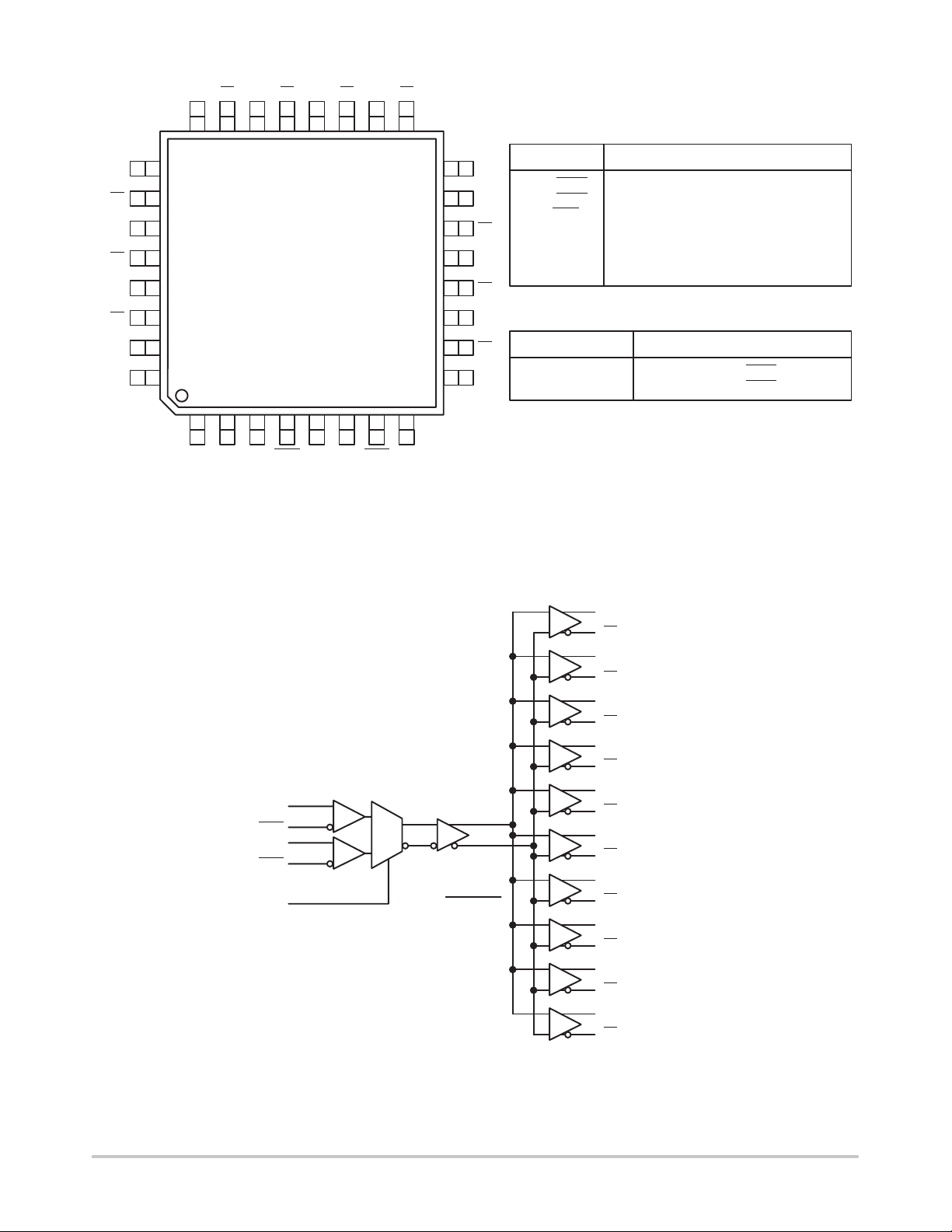
Q6Q6Q5Q5Q4Q4Q3 Q3
24 23 22 21 20 19 18 17
VCC
Q2
Q2
Q1
25
26
27
28
MC100LVEP111
Q1
Q0
Q0
VCC
29
30
31
32
12345678
VEECLK1CLK1VBBCLK0CLK0VCC
CLK_SEL
Figure 1. 32–Lead TQFP Pinout
(Top View)
Warning: All VCC and VEE pins must be externally connected
to Power Supply to guarantee proper operation.
PIN DESCRIPTION
16
15
14
13
12
11
10
9
VCC
Q7
Q7
Q8
Q8
Q9
Q9
VCC
Pins
CLK0, CLK0
CLK1, CLK1
Q0:9, Q0:9
CLK_SEL
VBB
VCC
VEE
CLK_SEL
0
1
LVECL/LVPECL/HSTL CLK Input
LVECL/LVPECL/HSTL CLK Input
LVECL/LVPECL Outputs
LVECL/LVPECL Active Clock Select Input
Reference Voltage Output
Positive Supply
Negative, 0 Supply
FUNCTION TABLE
Function
Active Input
CLK0, CLK0
CLK1, CLK1
CLK0
CLK0
CLK1
CLK1
CLK_SEL
Q
0
Q
0
Q
1
Q
1
Q
2
Q
2
Q
3
Q
3
Q
4
Q
0
1
V
BB
4
Q
5
Q
5
Q
6
Q
6
Q
7
Q
7
Q
8
Q
8
Q
9
Q
9
Figure 2. Logic Symbol
http://onsemi.com
2
Page 3
MC100LVEP111
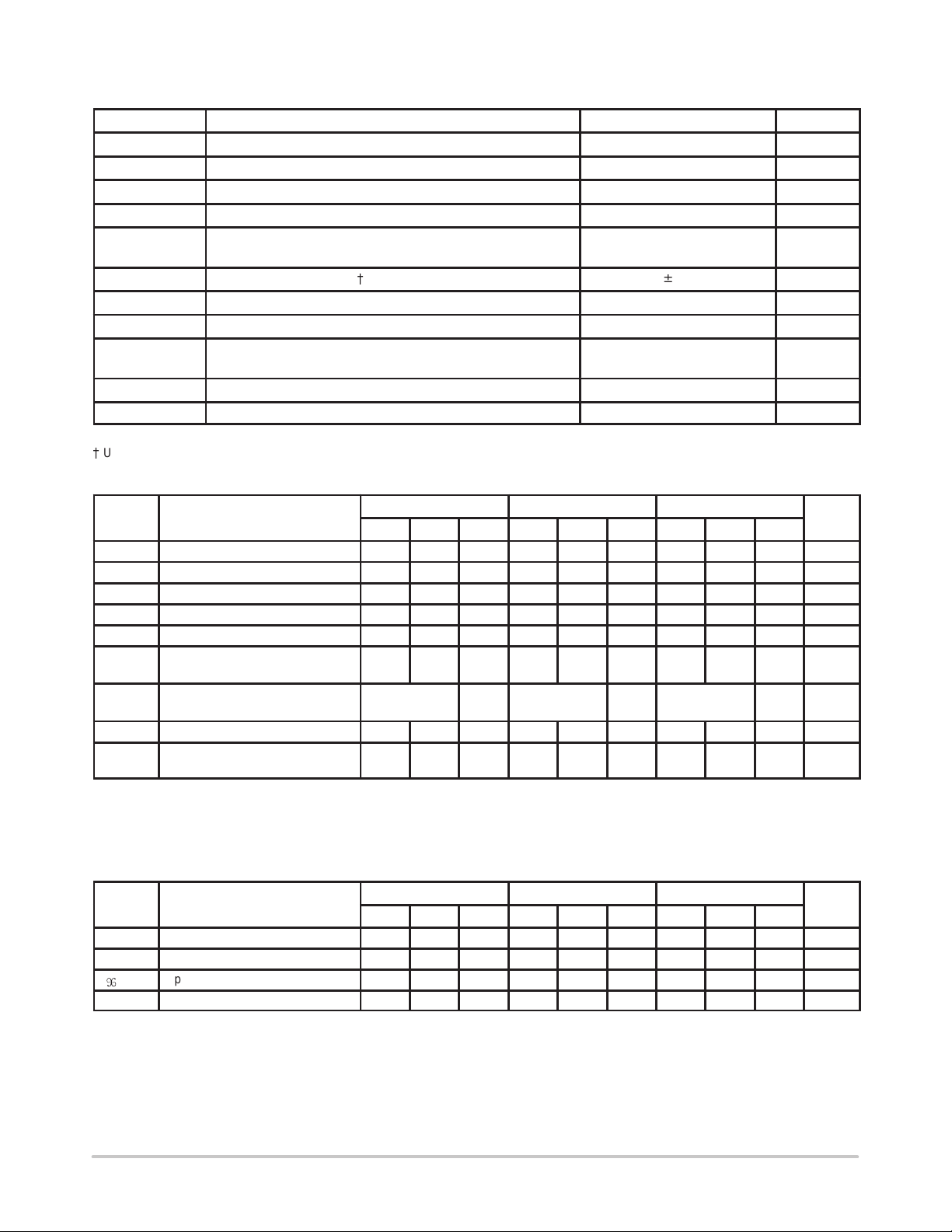
MAXIMUM RATINGS*
Symbol Parameter Value Unit
V
EE
V
CC
V
I
V
I
I
out
I
BB
T
A
T
stg
θ
JA
θ
JC
T
sol
* Maximum Ratings are those values beyond which damage to the device may occur.
{
Use for inputs of same package only.
DC CHARACTERISTICS, ECL/LVECL (VCC = 0V, VEE = –3.3(+0.925, –0.5)V) (Note 5.)
Symbol Characteristic Min Typ Max Min Typ Max Min Typ Max Unit
I
EE
V
OH
V
OL
V
IH
V
IL
V
BB
V
IHCMR
I
IH
I
IL
1. VCC = 0V, VEE = V
2. All loading with 50 ohms to VCC–2.0 volts.
3. Single ended input operation is limited VEE ≤ –3.0V in ECL/LVECL mode.
4. V
5. Input and output parameters vary 1:1 with VCC.
Power Supply Current (Note 1.) 70 100 120 70 100 120 70 100 120 mA
Output HIGH Voltage (Note 2.) –1145 –1020 –0895 –1145 –1020 –0895 –1 145 –1020 –0895 mV
Output LOW Voltage (Note 2.) –1995 –1820 –1650 –1995 –1820 –1650 –1995 –1820 –1650 mV
Input HIGH Voltage –1165 –0880 –1165 –0880 –1165 –0880 mV
Input LOW Voltage –1810 –1625 –1810 –1625 –1810 –1625 mV
Output Reference Voltage
(Note 3.)
Input HIGH Voltage Common
Mode Range (Note 4.)
Input HIGH Current 150 150 150 µA
Input LOW Current 0.5
min varies 1:1 with VEE, max varies 1:1 with VCC.
IHCMR
DC CHARACTERISTICS, HSTL (VCC = 2.5(–0.125, +1.3)V, VEE = 0V)
Symbol Characteristic Min Typ Max Min Typ Max Min Typ Max Unit
V
IH
V
IL
V
X
I
CC
6. VCC = 2.375V to 3.8V , VEE = 0V, all other pins floating.
Input HIGH Voltage 1200 mV
Input LOW Voltage 400 mV
Input Crossover Voltage 680 900 mV
Power Supply Current (Note 6.) 70 100 120 70 100 120 70 100 120 mA
Power Supply (VCC = 0V) –6.0 to 0 VDC
Power Supply (VEE = 0V) 6.0 to 0 VDC
Input Voltage (VCC = 0V, VI not more negative than VEE) –6.0 to 0 VDC
Input Voltage (VEE = 0V, VI not more positive than VCC) 6.0 to 0 VDC
Output Current Continuous
VBB Sink/Source Current
Operating Temperature Range –40 to +85 °C
Storage Temperature –65 to +150 °C
Thermal Resistance (Junction–to–Ambient) Still Air
Thermal Resistance (Junction–to–Case) 12 to 17 °C/W
Solder Temperature (<2 to 3 Seconds: 245°C desired) 265 °C
to V
EEmin
EEmax
{
–40°C 25°C 85°C
–1525 –1425 –1325 –1525 –1425 –1325 –1525 –1425 –1325 mV
VEE + 1.2 0.0 VEE + 1.2 0.0 VEE + 1.2 0.0 V
–150
, all other pins floating.
–40°C 25°C 85°C
Surge
500lfpm
0.5
–150
50
100
± 0.5 mA
80
55
0.5
–150
mA
°C/W
150 µA
http://onsemi.com
3
Page 4

MC100LVEP111
DC CHARACTERISTICS, LVPECL (VCC = 3.3V ± 0.5V, VEE = 0V) (Note 11.)
–40°C 25°C 85°C
Symbol Characteristic Min Typ Max Min Typ Max Min Typ Max Unit
I
EE
V
OH
V
OL
V
IH
V
IL
V
BB
V
IHCMR
I
IH
I
IL
7. V
8. All loading with 50 ohms to VCC–2.0 volts.
9. Single ended input operation is limited VCC ≥ 3.0V in PECL mode.
10.V
11.Input and output parameters vary 1:1 with VCC.
DC CHARACTERISTICS, LVEPECL (VCC = 2.5V ± 0.125V, VEE = 0V) (Note 15.)
Symbol Characteristic Min Typ Max Min Typ Max Min Typ Max Unit
I
EE
V
OH
V
OL
V
IH
V
IL
V
IHCMR
I
IH
I
IL
12.V
13.All loading with 50 ohms to VEE.
14.V
15.Input and output parameters vary 1:1 with VCC.
AC CHARACTERISTICS (VCC = 0V; VEE = –2.5(+0.125, –1.3)V)
Symbol Characteristic Min Typ Max Min Typ Max Min Typ Max Unit
f
maxLVPECL
f
maxHSTL
t
PLH
t
PHL
t
skew
V
PP
tr/t
f
16.F
17.Skew is measured between outputs under identical transitions and conditions on any one device.
18.Part–to–part skew for identical transitions at identical VCC levels.
Power Supply Current (Note 7.) 70 100 120 70 100 120 70 100 120 mA
Output HIGH Voltage (Note 8.) 2155 2280 2405 2155 2280 2405 2155 2280 2405 mV
Output LOW Voltage (Note 8.) 1305 1480 1650 1305 1480 1650 1305 1480 1650 mV
Input HIGH Voltage 2135 2420 2135 2420 2135 2420 mV
Input LOW Voltage 1490 1675 1490 1675 1490 1675 mV
Output Reference Voltage
(Note 9.)
Input HIGH Voltage Common
Mode Range (Note 10.)
Input HIGH Current 150 150 150 µA
Input LOW Current 0.5
to V
CCmin
min varies 1:1 with VEE, max varies 1:1 with VCC.
IHCMR
Power Supply Current (Note 12.) 70 100 120 70 100 120 70 100 120 mA
Output HIGH Voltage (Note 13.) 1355 1480 1605 1355 1480 1605 1355 1480 1605 mV
Output LOW Voltage (Note 13.) 505 680 850 505 680 850 505 680 850 mV
Input HIGH Voltage 1335 1620 1335 1620 1335 1620 mV
Input LOW Voltage 690 875 690 875 690 875 mV
Input HIGH Voltage Common
Mode Range (Note 14.)
Input HIGH Current 150 150 150 µA
Input LOW Current 0.5
to V
CCmin
min varies 1:1 with VEE, max varies 1:1 with VCC.
IHCMR
guaranteed for functionality only.
max
.
CCmax
.
CCmax
Maximum Input Frequency
for LVECL and LVPECL
Maximum Input Frequency
for HSTL
Propagation Delay to Output
IN (differential)
Within–Device Skew (17.)
Part–to–Part Skew (Diff) (18.)
Minimum Input Swing 150 800 1200 150 800 1200 150 800 1200 mV
Output Rise/Fall Time
(20%–80%)
1775 1875 1975 1775 1875 1975 1775 1875 1975 mV
1.2 3.3 1.2 3.3 1.2 3.3 V
–150
–40°C 25°C 85°C
1.2 2.5 1.2 2.5 1.2 2.5 V
–150
–40°C 25°C 85°C
1.5 1.5 1.5 GHz
250 250 250 MHz
300 400 500 310 430 550 350 510 625 ps
20
100
100 180 300 120 200 320 130 230 375 ps
0.5
–150
0.5
–150
20
100
25 20
0.5
–150
0.5
–150
100
150 µA
150 µA
ps
http://onsemi.com
4
Page 5

MC100LVEP111
P ACKAGE DIMENSIONS
FA SUFFIX
PLASTIC TQFP PACKAGE
CASE 873A–02
ISSUE A
9
SEATING
PLANE
C
B1
–T–
–AB–
–AC–
E
–Z–
X
4X
25
–U–
V1
17
4X
T–U0.20 (0.008) ZAB
BASE
METAL
N
VB
DF
J
SECTION AE–AE
T–U0.20 (0.008) Z
AC
DETAIL AD
R
AE
P
AE
DETAIL Y
_
Q
K
0.250 (0.010)
GAUGE PLANE
NOTES:
1. DIMENSIONING AND TOLERANCING PER ANSI
Y14.5M, 1982.
2. CONTROLLING DIMENSION: MILLIMETER.
T–U
3. DATUM PLANE –AB– IS LOCATED AT BOTTOM
OF LEAD AND IS COINCIDENT WITH THE LEAD
WHERE THE LEAD EXITS THE PLASTIC BODY AT
M
THE BOTTOM OF THE PARTING LINE.
4. DATUMS –T–, –U–, AND –Z– TO BE
DETERMINED AT DATUM PLANE –AB–.
5. DIMENSIONS S AND V TO BE DETERMINED AT
SEATING PLANE –AC–.
6. DIMENSIONS A AND B DO NOT INCLUDE
MOLD PROTRUSION. ALLOWABLE PROTRUSION
0.20 (0.008) ZAC
IS 0.250 (0.010) PER SIDE. DIMENSIONS A AND B
DO INCLUDE MOLD MISMATCH AND ARE
DETERMINED AT DATUM PLANE –AB–.
7. DIMENSION D DOES NOT INCLUDE DAMBAR
PROTRUSION. DAMBAR PROTRUSION SHALL
NOT CAUSE THE D DIMENSION TO EXCEED
0.520 (0.020).
8. MINIMUM SOLDER PLATE THICKNESS SHALL
BE 0.0076 (0.0003).
9. EXACT SHAPE OF EACH CORNER MAY VARY
FROM DEPICTION.
MILLIMETERS
DIMAMIN MAX MIN MAX
7.000 BSC 0.276 BSC
A1 3.500 BSC 0.138 BSC
B 7.000 BSC 0.276 BSC
–T–, –U–, –Z–
B1 3.500 BSC 0.138 BSC
C 1.400 1.600 0.055 0.063
D 0.300 0.450 0.012 0.018
E 1.350 1.450 0.053 0.057
F 0.300 0.400 0.012 0.016
G 0.800 BSC 0.031 BSC
H 0.050 0.150 0.002 0.006
J 0.090 0.200 0.004 0.008
K 0.500 0.700 0.020 0.028
__
M 12 REF 12 REF
N 0.090 0.160 0.004 0.006
P 0.400 BSC 0.016 BSC
Q 1 5 1 5
___ _
R 0.150 0.250 0.006 0.010
S 9.000 BSC 0.354 BSC
S1 4.500 BSC 0.177 BSC
V 9.000 BSC 0.354 BSC
V1 4.500 BSC 0.177 BSC
W 0.200 REF 0.008 REF
X 1.000 REF 0.039 REF
INCHES
A
A1
32
1
DETAIL Y
8
9
S1
S
G
0.10 (0.004) AC
_
M
8X
H
W
DETAIL AD
http://onsemi.com
5
Page 6

Notes
MC100LVEP111
http://onsemi.com
6
Page 7

Notes
MC100LVEP111
http://onsemi.com
7
Page 8

MC100LVEP111
ON Semiconductor and are trademarks of Semiconductor Components Industries, LLC (SCILLC). SCILLC reserves the right to make changes
without further notice to any products herein. SCILLC makes no warranty , representation or guarantee regarding the suitability of its products for any particular
purpose, nor does SCILLC assume any liability arising out of the application or use of any product or circuit, and specifically disclaims any and all liability ,
including without limitation special, consequential or incidental damages. “Typical” parameters which may be provided in SCILLC data sheets and/or
specifications can and do vary in different applications and actual performance may vary over time. All operating parameters, including “Typicals” must be
validated for each customer application by customer’s technical experts. SCILLC does not convey any license under its patent rights nor the rights of others.
SCILLC products are not designed, intended, or authorized for use as components in systems intended for surgical implant into the body, or other applications
intended to support or sustain life, or for any other application in which the failure of the SCILLC product could create a situation where personal injury or
death may occur. Should Buyer purchase or use SCILLC products for any such unintended or unauthorized application, Buyer shall indemnify and hold
SCILLC and its officers, employees, subsidiaries, affiliates, and distributors harmless against all claims, costs, damages, and expenses, and reasonable
attorney fees arising out of, directly or indirectly , any claim of personal injury or death associated with such unintended or unauthorized use, even if such claim
alleges that SCILLC was negligent regarding the design or manufacture of the part. SCILLC is an Equal Opportunity/Affirmative Action Employer .
PUBLICATION ORDERING INFORMATION
NORTH AMERICA Literature Fulfillment:
Literature Distribution Center for ON Semiconductor
P.O. Box 5163, Denver, Colorado 80217 USA
Phone: 303–675–2175 or 800–344–3860 Toll Free USA/Canada
Fax: 303–675–2176 or 800–344–3867 Toll Free USA/Canada
Email: ONlit@hibbertco.com
Fax Response Line: 303–675–2167 or 800–344–3810 T oll Free USA/Canada
N. American Technical Support: 800–282–9855 Toll Free USA/Canada
EUROPE: LDC for ON Semiconductor – European Support
German Phone: (+1) 303–308–7140 (M–F 1:00pm to 5:00pm Munich Time)
Email: ONlit–german@hibbertco.com
French Phone: (+1) 303–308–7141 (M–F 1:00pm to 5:00pm Toulouse Time)
Email: ONlit–french@hibbertco.com
English Phone: (+1) 303–308–7142 (M–F 12:00pm to 5:00pm UK Time)
Email: ONlit@hibbertco.com
EUROPEAN TOLL–FREE ACCESS*: 00–800–4422–3781
*Available from Germany, France, Italy, England, Ireland
CENTRAL/SOUTH AMERICA:
Spanish Phone: 303–308–7143 (Mon–Fri 8:00am to 5:00pm MST)
Email: ONlit–spanish@hibbertco.com
ASIA/PACIFIC : LDC for ON Semiconductor – Asia Support
Phone: 303–675–2121 (Tue–Fri 9:00am to 1:00pm, Hong Kong Time)
T oll Free from Hong Kong & Singapore:
001–800–4422–3781
Email: ONlit–asia@hibbertco.com
JAPAN: ON Semiconductor, Japan Customer Focus Center
4–32–1 Nishi–Gotanda, Shinagawa–ku, T okyo, Japan 141–8549
Phone: 81–3–5740–2745
Email: r14525@onsemi.com
ON Semiconductor Website: http://onsemi.com
For additional information, please contact your local
Sales Representative.
http://onsemi.com
8
MC100L VEP11 1/D
 Loading...