

Page 1
MC100LVEL32
÷
2 Divider
The MC100LVEL32 is an integrated ÷2 divider. The differential
clock inputs and the VBB allow a differential, single-ended or AC
coupled interface to the device. If used, the VBB output should be
bypassed to ground with a 0.01µF capacitor . Also note that the VBB is
designed to be used as an input bias on the LVEL32 only, the V
output has limited current sink and source capability.The LVEL32 is
functionally identical to the EL32, but operates from a low voltage
supply.
The reset pin is asynchronous and is asserted on the rising edge.
Upon power-up, the internal flip-flop will attain a random state; the
reset allows for the synchronization of multiple EL32’s in a system.
• 510ps Propagation Delay
• 3.0GHz T oggle Frequency
• High Bandwidth Output Transitions
• 75kΩ Internal Input Pulldown Resistors
• >1000V ESD Protection
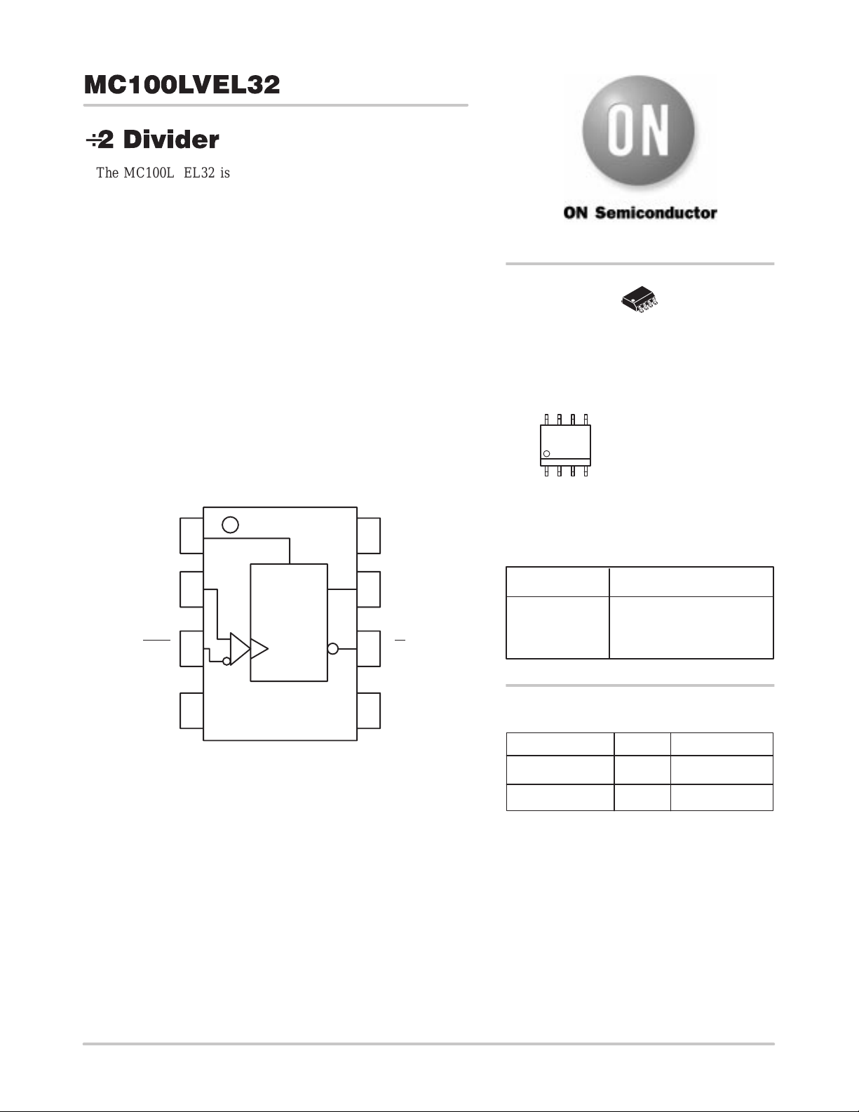
LOGIC DIAGRAM AND PINOUT ASSIGNMENT
Reset
CLK
1
R
2
÷2
3
78Q
6
V
CC
QCLK
BB
http://onsemi.com
8
1
SO–8
D SUFFIX
CASE 751
MARKING DIAGRAM
8
KVL32
ALYW
1
*For additional information, see Application Note
AND8002/D
PIN FUNCTION
CLK Clock Inputs
Reset Asynch Reset
V
BB
Q Data Ouputs
A = Assembly Location
L = Wafer Lot
Y = Year
W = Work Week
PIN DESCRIPTION
Ref Voltage Output
BB
4
V
Semiconductor Components Industries, LLC, 2000
April, 2000 – Rev. 1
5
V
EE
MC100L VEL32D SO–8 98 Units/Rail
MC100L VEL32DR2 SO–8 2500 Tape & Reel
1 Publication Order Number:
ORDERING INFORMATION
Device Package Shipping
MC100L VEL32/D
Page 2
MC100LVEL32
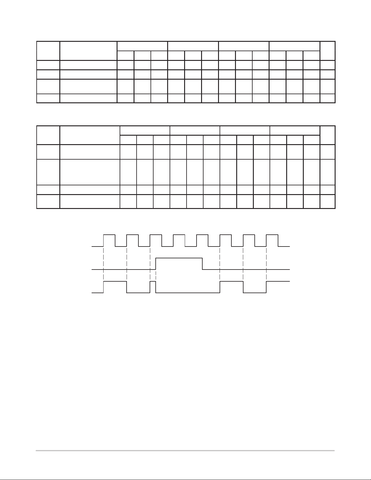
DC CHARACTERISTICS (VEE = VEE(min) to VEE(max); VCC = GND)
–40°C 0°C 25°C 85°C
Symbol Characteristic Min Typ Max Min Typ Max Min Typ Max Min Typ Max Unit
I
EE
V
EE
V
BB
I
IH
AC CHARACTERISTICS (VEE = VEE(min) to VEE(max); VCC = GND)
Symbol Characteristic Min Typ Max Min Typ Max Min Typ Max Min Typ Max Unit
f
MAX
t
PLH
t
PHL
V
PP
t
r
t
f
1. Minimum input swing for which AC parameters are guaranteed.
Power Supply Current 25 25 25 25 mA
Power Supply Voltage –3.0 –3.0 –3.3 –3.8 –3.0 –3.3 –3.8 –3.0 –3.3 –3.8 V
Output Reference
Voltage
Input HIGH Current 150 150 150 150 µA
Maximum Toggle
Frequency
Propagation Delay
CLK to Q (Diff)
CLK to Q (S.E.)
Reset to Q
Minimum Input Swing
Output Rise/Fall Times Q
(20% – 80%)
–1.38 –1.26 –1.38 –1.26 –1.38 –1.26 –1.38 –1.26 V
–40°C 0°C 25°C 85°C
3.0 3.0 3.0 3.0 GHz
350
500
530
360
500
540
370
510
550
410
300
500
580
310
500
590
320
510
340
540
540
350
540
550
350
1
150 150 150 150 mV
225 225 225 225 ps
540
600
550
360
380
540
540
550
590
640
580
ps
CLK
RESET
Q
Figure 1. Timing Diagram
http://onsemi.com
2
Page 3

MC100LVEL32
P ACKAGE DIMENSIONS
SO–8
D SUFFIX
PLASTIC SOIC PACKAGE
CASE 751–06
ISSUE T
A
E
B
C
A1
D
58
0.25MB
1
H
4
e
M
h
X 45
_
q
C
A
SEATING
PLANE
0.10
L
B
SS
A0.25MCB
NOTES:
1. DIMENSIONING AND TOLERANCING PER ASME
Y14.5M, 1994.
2. DIMENSIONS ARE IN MILLIMETER.
3. DIMENSION D AND E DO NOT INCLUDE MOLD
PROTRUSION.
4. MAXIMUM MOLD PROTRUSION 0.15 PER SIDE.
5. DIMENSION B DOES NOT INCLUDE DAMBAR
PROTRUSION. ALLOWABLE DAMBAR
PROTRUSION SHALL BE 0.127 TOTAL IN EXCESS
OF THE B DIMENSION AT MAXIMUM MATERIAL
CONDITION.
MILLIMETERS
DIM MIN MAX
A 1.35 1.75
A1 0.10 0.25
B 0.35 0.49
C 0.19 0.25
D 4.80 5.00
E
3.80 4.00
1.27 BSCe
H 5.80 6.20
h
0.25 0.50
L 0.40 1.25
0 7
q
__
http://onsemi.com
3
Page 4

MC100LVEL32
ON Semiconductor and are trademarks of Semiconductor Components Industries, LLC (SCILLC). SCILLC reserves the right to make changes
without further notice to any products herein. SCILLC makes no warranty , representation or guarantee regarding the suitability of its products for any particular
purpose, nor does SCILLC assume any liability arising out of the application or use of any product or circuit, and specifically disclaims any and all liability ,
including without limitation special, consequential or incidental damages. “Typical” parameters which may be provided in SCILLC data sheets and/or
specifications can and do vary in different applications and actual performance may vary over time. All operating parameters, including “Typicals” must be
validated for each customer application by customer’s technical experts. SCILLC does not convey any license under its patent rights nor the rights of others.
SCILLC products are not designed, intended, or authorized for use as components in systems intended for surgical implant into the body, or other applications
intended to support or sustain life, or for any other application in which the failure of the SCILLC product could create a situation where personal injury or
death may occur. Should Buyer purchase or use SCILLC products for any such unintended or unauthorized application, Buyer shall indemnify and hold
SCILLC and its officers, employees, subsidiaries, affiliates, and distributors harmless against all claims, costs, damages, and expenses, and reasonable
attorney fees arising out of, directly or indirectly , any claim of personal injury or death associated with such unintended or unauthorized use, even if such claim
alleges that SCILLC was negligent regarding the design or manufacture of the part. SCILLC is an Equal Opportunity/Affirmative Action Employer .
PUBLICATION ORDERING INFORMATION
NORTH AMERICA Literature Fulfillment:
Literature Distribution Center for ON Semiconductor
P.O. Box 5163, Denver, Colorado 80217 USA
Phone: 303–675–2175 or 800–344–3860 Toll Free USA/Canada
Fax: 303–675–2176 or 800–344–3867 Toll Free USA/Canada
Email: ONlit@hibbertco.com
Fax Response Line: 303–675–2167 or 800–344–3810 T oll Free USA/Canada
N. American Technical Support: 800–282–9855 Toll Free USA/Canada
EUROPE: LDC for ON Semiconductor – European Support
German Phone: (+1) 303–308–7140 (M–F 1:00pm to 5:00pm Munich Time)
Email: ONlit–german@hibbertco.com
French Phone: (+1) 303–308–7141 (M–F 1:00pm to 5:00pm Toulouse T ime)
Email: ONlit–french@hibbertco.com
English Phone: (+1) 303–308–7142 (M–F 12:00pm to 5:00pm UK Time)
Email: ONlit@hibbertco.com
EUROPEAN TOLL–FREE ACCESS*: 00–800–4422–3781
*Available from Germany, France, Italy, England, Ireland
CENTRAL/SOUTH AMERICA:
Spanish Phone: 303–308–7143 (Mon–Fri 8:00am to 5:00pm MST)
Email: ONlit–spanish@hibbertco.com
ASIA/PACIFIC : LDC for ON Semiconductor – Asia Support
Phone: 303–675–2121 (Tue–Fri 9:00am to 1:00pm, Hong Kong Time)
T oll Free from Hong Kong & Singapore:
001–800–4422–3781
Email: ONlit–asia@hibbertco.com
JAPAN: ON Semiconductor, Japan Customer Focus Center
4–32–1 Nishi–Gotanda, Shinagawa–ku, T okyo, Japan 141–8549
Phone: 81–3–5740–2745
Email: r14525@onsemi.com
ON Semiconductor Website: http://onsemi.com
For additional information, please contact your local
Sales Representative.
http://onsemi.com
4
MC100L VEL32/D
 Loading...