

Page 1

SEMICONDUCTOR TECHNICAL DATA
÷÷
ECL fanout buffer designed with clock distribution in mind. The device
features fully differential clock paths to minimize both device and system
skew. The LVE222 can be used as a simple fanout buffer or outputs can
be configured to provide half frequency outputs. The combination of 1x
and 1/2x frequencies is flexible providing for a myriad of combinations. All
timing differences between the 1x and 1/2x signals are compensated for
internal to the chip so that the output–to–output skew is identical
regardless of what output frequencies are selected.
The MC100LVE222 is a low voltage, low skew 1:15 differential ÷1/÷2
• Fifteen Differential Outputs
• 200ps Part–to–Part Skew
• 50ps Output–to–Output Skew
• Selectable 1x or 1/2x Frequency Outputs
• Extended Power Supply Range of –3.0V to –5.25V (+3.0V to +5.25V)
• 52–Lead TQFP Packaging
• ESD > 2000V
The fsel and CLK_Sel input pins are asynchronous control signals. As
a result, changing these inputs could cause indeterminent excursions on
the outputs immediately following the changes on the inputs.
For applications which require a single–ended input, the VBB reference
voltage is supplied. For single–ended input applications the V
reference should be connected to the CLK
via a 0.01µf capacitor. The input signal is then driven into the CLK input.
To ensure that the tight skew specification is met it is necessary that both sides of the differential output are terminated into
50Ω, even if only one side is being used. In most applications all fifteen dif ferential pairs will be used and therefore terminated. In
the case where fewer than fifteen pairs are used it is necessary to terminate at least the output pairs adjacent to the output pair
being used in order to maintain minimum skew. Failure to follow this guideline will result in small degradations of propagation
delay (on the order of 10–20ps) of the outputs being used, while not catastrophic to most designs this will result in an increase in
skew. Note that the package corners isolate outputs from one another such that the guideline expressed above holds only for
outputs on the same side of the package.
The MC100L VE222, as with most ECL devices, can be operated from a positive VCC supply in PECL mode. This allows the
LVE222 to be used for high performance clock distribution in +3.3V systems. Designers can take advantage of the LVE222’s
performance to distribute low skew clocks across the backplane or the board. In a PECL environment series or Thevenin line,
terminations are typically used as they require no additional power supplies, if parallel termination is desired a terminating voltage
of VCC–2.0V will need to be provided. For more information on using PECL, designers should refer to Motorola Application Note
AN1406/D.
The MC100LVE222 is packaged in the 52–lead TQFP package. For a 3.3V supply this package provides the optimum
performance and minimizes board space requirements. The LVE222 will operate from a standard 100E –4.5V supply or a 5.0V
PECL supply. The 52–lead TQFP utilizes a 10x10mm body with a lead pitch of 0.65mm.
input and bypassed to ground
BB
LOW VOLTAGE
1:15 DIFFERENTIAL ÷1/÷2
ECL/PECL CLOCK DRIVER
FA SUFFIX
TQFP PACKAGE
CASE 848D–03
10/96
Motorola, Inc. 1996
4–1
REV 1
Page 2
MC100LVE222
VCCO
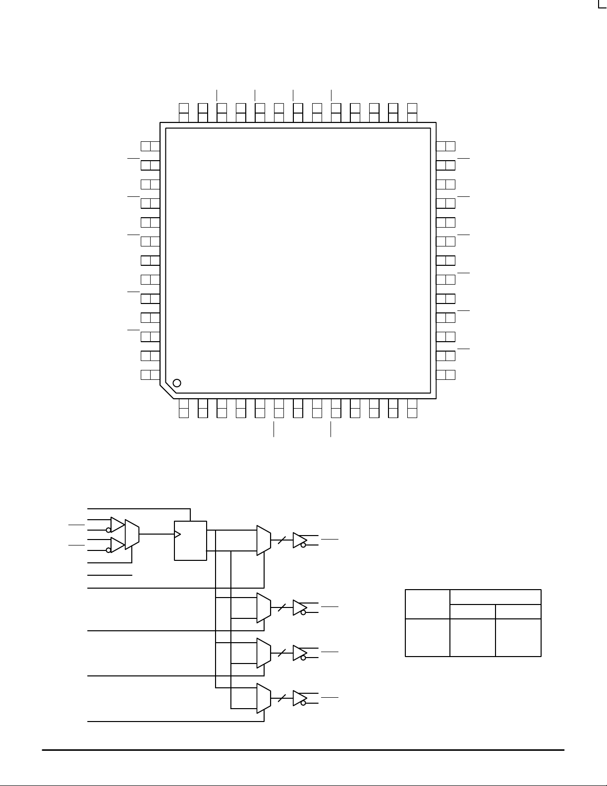
Pinout: 52–Lead TQFP (Top View)
VCCO
Qc0
Qc0
Qc1
Qc1
Qc2
Qc2
Qc3
Qc3
VCCONCNC
39 38 37 36 35 34 33 32 31 30 29 28 27
40
VCCO
26
Qd0
Qb2
Qb2
Qb1
Qb1
Qb0
Qb0
VCCO
Qa1
Qa1
Qa0
Qa0
VCCO
41
42
43
44
45
46
47
48
49
50
51
52
12345678910111213
MR
VCC
fsela
MC100LVE222
fselb
CLK0
CLK0
CLK1
CLK_Sel
CLK1
VBB
fselc
fseld
25
24
23
22
21
20
19
18
17
16
15
14
VEE
Qd0
Qd1
Qd1
Qd2
Qd2
Qd3
Qd3
Qd4
Qd4
Qd5
Qd5
VCCO
LOGIC SYMBOL
MR
CLK0
CLK0
CLK1
CLK1
CLK_Sel
V
BB
fsela
fselb
fselc
fseld
MOTOROLA ECLinPS and ECLinPS Lite
÷
1
÷
2
2
Qa0:1
Qa0:1
FUNCTION TABLE
3
4
6
4–2
Qb0:2
Qb0:2
Qc0:3
Qc0:3
Qd0:5
Qd0:5
Input
MR
CLK_Sel
fseln
Function
01
Active
CLK0
÷1
Reset
CLK1
÷2
DL140 — Rev 3
Page 3

MC100LVE222
ECL DC CHARACTERISTICS
–40°C 0°C 25°C 70°C
Symbol Characteristic Min Typ Max Min Typ Max Min Typ Max Min Typ Max Unit
V
OH
V
OL
V
IH
V
IL
V
BB
V
EE
I
IH
I
IL
I
EE
PECL DC CHARACTERISTICS
Symbol Characteristic Min Typ Max Min Typ Max Min Typ Max Min Typ Max Unit
V
OH
V
OL
V
IH
V
IL
V
BB
V
CC
I
IH
I
IL
I
EE
1. These values are for VCC = 3.3V. Level Specifications will vary 1:1 with VCC.
Output HIGH Voltage –1.085 –1.005 –0.880 –1.025 –0.955 –0.880 –1.025 –0.955 –0.880 –1.025 –0.955 –0.880 V
Output LOW Voltage –1.830 –1.695 –1.555 –1.810 –1.705 –1.620 –1.810 –1.705 –1.620 –1.810 –1.705 –1.620 V
Input HIGH Voltage –1.165 –0.880 –1.165 –0.880 –1.165 –0.880 –1.165 –0.880 V
Input LOW Voltage –1.810 –1.475 –1.810 –1.475 –1.810 –1.475 –1.810 –1.475 V
Output Reference
Voltage
Power Supply Voltage –3.0 –5.25 –3.0 –5.25 –3.0 –5.25 –3.0 –5.25 V
Input HIGH Current 150 150 150 150 µA
Input CLK0, CLK1
LOW Current Others
Power Supply Current 122 136 122 136 122 136 125 139 mA
Output HIGH Voltage
Output LOW Voltage
Input HIGH Voltage
Input LOW Voltage
Output Reference
1.
Voltage
Power Supply Voltage 3.0 5.25 3.0 5.25 3.0 5.25 3.0 5.25 V
Input HIGH Current 150 150 150 150 µA
Input CLK0, CLK1
LOW Current Others
Power Supply Current 122 136 122 136 122 136 125 139 mA
–1.38 –1.26 –1.38 –1.26 –1.38 –1.26 –1.38 –1.26 V
–300
0.5
–40°C 0°C 25°C 70°C
1.
2.215 2.295 2.420 2.275 2.345 2.420 2.275 2.345 2.420 2.275 2.345 2.420 V
1.
1.470 1.605 1.745 1.490 1.595 1.680 1.490 1.595 1.680 1.490 1.595 1.680 V
1.
1.
2.135 2.420 2.135 2.420 2.135 2.420 2.135 2.420 V
1.490 1.825 1.490 1.825 1.490 1.825 1.490 1.825 V
1.92 2.04 1.92 2.04 1.92 2.04 1.92 2.04 V
–300
0.5
–300
0.5
–300
0.5
–300
0.5
–300
0.5
–300
0.5
–300
0.5
µA
µA
DL140 — Rev 3
4–3 MOTOROLAECLinPS and ECLinPS Lite
Page 4

MC100LVE222
ECL AC CHARACTERISTICS (VEE = VEE (min) to VEE (max); VCC = V
–40°C 0°C 25°C 70°C
Symbol Characteristic Min Typ Max Min Typ Max Min Typ Max Min Typ Max Unit Condition
t
PLH
t
PHL
t
skew
V
PP
V
CMR
tr/t
Propagation Delay to Output
Within–Device Skew
Part–to–Part Skew (Diff)
Minimum Input Swing 400 400 400 400 mV Note 4.
Common Mode Range
Output Rise/Fall Time 200 600 200 600 200 600 200 600 ps 20%–80%
f
IN (differential)
IN (single–ended)
VPP < 500mV
VPP ≥ 500mV V
MR
1040
990
1100
V
EE
+1.3
EE
+1.6
1140
1140
1250
1240
1290
1400
50
200
–0.4 V
–0.4 V
1060
1010
1130
EE
+1.2
EE
+1.5
1160
1160
1280
1260
1310
1430
50
200
–0.4 V
–0.4 V
1080
1030
1170
+1.2
+1.5
EE
EE
CCO
1180
1180
1320
= GND)
1280
1330
1470
50
200
–0.4 V
–0.4 V
1120
1070
1220
EE
+1.2
EE
+1.5
1220
1220
1370
1320
1370
1520
50
200
–0.4
–0.4
ps
Note 1.
Note 2.
ps Note 3.
V Note 5.
1. The differential propagation delay is defined as the delay from the crossing points of the differential input signals to the crossing point of the
differential output signals. See
Definitions and T esting of ECLinPS AC Parameters
in Chapter 1 (page 1–12) of the Motorola High Performance
ECL Data Book (DL140/D).
2. The single-ended propagation delay is defined as the delay from the 50% point of the input signal to the 50% point of the output signal. See
Definitions and T esting of ECLinPS AC Parameters
in Chapter 1 (page 1–12) of the Motorola High Performance ECL Data Book (DL140/D).
3. The within–device skew is defined as the worst case difference between any two similar delay paths within a single device.
4. VPP(min) is defined as the minimum input differential voltage which will cause no increase in the propagation delay . The VPP(min) is AC limited
for the LVE222. A differential input as low as 50 mV will still produce full ECL levels at the output.
5. V
is defined as the range within which the VIH level may vary, with the device still meeting the propagation delay specification. The VIL level
CMR
must be such that the peak to peak voltage is less than 1.0 V and greater than or equal to VPP(min).
PECL AC CHARACTERISTICS (VEE = GND; VCC = V
–40°C 0°C 25°C 70°C
Symbol Characteristic Min Typ Max Min Typ Max Min Typ Max Min Typ Max Unit Condition
t
PLH
t
PHL
t
skew
V
PP
V
CMR
tr/t
Propagation Delay to Output
Within–Device Skew
Part–to–Part Skew (Diff)
Minimum Input Swing 400 400 400 400 mV Note 4.
Common Mode Range
Output Rise/Fall Time 200 600 200 600 200 600 200 600 ps 20%–80%
f
IN (differential)
IN (single–ended)
VPP < 500mV
VPP ≥ 500mV 1.6 V
MR
1040
1100
1140
990
1140
1250
1.3 V
1240
1290
1400
50
200
CC
–0.4
CC
–0.4
1060
1010
1130
1.2 V
1.5 V
= VCC (min) to VCC (max))
CCO
1160
1260
1080
1160
1280
1310
1430
50
200
CC
–0.4
CC
–0.4
1180
1030
1180
1170
1320
1.2 V
1.5 V
1280
1330
1470
50
200
CC
–0.4
CC
–0.4
1120
1220
1070
1220
1220
1370
1.2 V
1.5 V
1320
1370
1520
50
200
CC
–0.4
CC
–0.4
ps
Note 1.
Note 2.
ps Note 3.
V Note 5.
1. The differential propagation delay is defined as the delay from the crossing points of the differential input signals to the crossing point of the
differential output signals. See
Definitions and T esting of ECLinPS AC Parameters
in Chapter 1 (page 1–12) of the Motorola High Performance
ECL Data Book (DL140/D).
2. The single-ended propagation delay is defined as the delay from the 50% point of the input signal to the 50% point of the output signal. See
Definitions and T esting of ECLinPS AC Parameters
in Chapter 1 (page 1–12) of the Motorola High Performance ECL Data Book (DL140/D).
3. The within–device skew is defined as the worst case difference between any two similar delay paths within a single device.
4. VPP(min) is defined as the minimum input differential voltage which will cause no increase in the propagation delay . The VPP(min) is AC limited
for the LVE222. A differential input as low as 50 mV will still produce full ECL levels at the output.
5. V
is defined as the range within which the VIH level may vary, with the device still meeting the propagation delay specification. The VIL level
CMR
must be such that the peak to peak voltage is less than 1.0 V and greater than or equal to VPP(min).
MOTOROLA ECLinPS and ECLinPS Lite
4–4
DL140 — Rev 3
Page 5

MC100LVE222
OUTLINE DIMENSIONS
FA SUFFIX
TQFP PACKAGE
CASE 848D–03
ISSUE C
–X–
4X
N0.20 (0.008) H L–M N0.20 (0.008) T L–M
4X TIPS
C
L
AB
4052
1
39
AB
X=L, M, N
G
–L–
–H–
–T–
SEATING
PLANE
3X VIEW Y
–M–
B V
B1
V1
13
14
A1
–N–
27
26
S1
A
S
C
4X θ2
0.10 (0.004) T
4X θ3
VIEW AA
0.05 (0.002)
C2
S
W
θ1
2 X R R1
0.25 (0.010)
θ
GAGE PLANE
PLATING
0.13 (0.005) N
ROTATED 90_ CLOCKWISE
NOTES:
1 DIMENSIONING AND TOLERANCING PER ANSI
Y14.5M, 1982.
2 CONTROLLING DIMENSION: MILLIMETER.
3 DATUM PLANE –H– IS LOCATED AT BOTTOM OF
LEAD AND IS COINCIDENT WITH THE LEAD
WHERE THE LEAD EXITS THE PLASTIC BODY AT
THE BOTTOM OF THE PARTING LINE.
4 DATUMS –L–, –M– AND –N– TO BE DETERMINED
AT DATUM PLANE –H–.
5 DIMENSIONS S AND V TO BE DETERMINED AT
SEATING PLANE –T–.
6 DIMENSIONS A AND B DO NOT INCLUDE MOLD
PROTRUSION. ALLOWABLE PROTRUSION IS
0.25 (0.010) PER SIDE. DIMENSIONS A AND B DO
INCLUDE MOLD MISMATCH AND ARE
DETERMINED AT DATUM PLANE -H-.
7 DIMENSION D DOES NOT INCLUDE DAMBAR
PROTRUSION. DAMBAR PROTRUSION SHALL
NOT CAUSE THE LEAD WIDTH TO EXCEED 0.46
(0.018). MINIMUM SPACE BETWEEN
PROTRUSION AND ADJACENT LEAD OR
PROTRUSION 0.07 (0.003).
K
C1
E
Z
VIEW AA
VIEW Y
F
J
BASE METAL
U
D
M
S
L–M
T
SECTION AB–AB
MILLIMETERS
DIMAMIN MAX MIN MAX
10.00 BSC 0.394 BSC
A1 5.00 BSC 0.197 BSC
B 10.00 BSC 0.394 BSC
B1 5.00 BSC 0.197 BSC
C ––– 1.70 ––– 0.067
C1 0.05 0.20 0.002 0.008
C2 1.30 1.50 0.051 0.059
D 0.20 0.40 0.008 0.016
E 0.45 0.030
F 0.22 0.35 0.009 0.014
G 0.65 BSC
J 0.07 0.20 0.003 0.008
K 0.50 REF 0.020 REF
R1 0.08 0.20 0.003 0.008
S 12.00 BSC 0.472 BSC
S1 6.00 BSC 0.236 BSC
U 0.09 0.16 0.004 0.006
V 12.00 BSC 0.472 BSC
V1 6.00 BSC 0.236 BSC
W 0.20 REF 0.008 REF
Z 1.00 REF 0.039 REF
θ
07
__
θ
1
0
_
12
θ
2
θ
3
REF
_
513
_
INCHES
0.75 0.018
0.026 BSC
07
__
––– –––
0
_
12
REF
_
5
_
13
_
S
_
DL140 — Rev 3
4–5 MOTOROLAECLinPS and ECLinPS Lite
Page 6

MC100LVE222
Motorola reserves the right to make changes without further notice to any products herein. Motorola makes no warranty , representation or guarantee regarding
the suitability of its products for any particular purpose, nor does Motorola assume any liability arising out of the application or use of any product or circuit, and
specifically disclaims any and all liability, including without limitation consequential or incidental damages. “T ypical” parameters which may be provided in Motorola
data sheets and/or specifications can and do vary in different applications and actual performance may vary over time. All operating parameters, including “Typicals”
must be validated for each customer application by customer’s technical experts. Motorola does not convey any license under its patent rights nor the rights of
others. Motorola products are not designed, intended, or authorized for use as components in systems intended for surgical implant into the body, or other
applications intended to support or sustain life, or for any other application in which the failure of the Motorola product could create a situation where personal injury
or death may occur. Should Buyer purchase or use Motorola products for any such unintended or unauthorized application, Buyer shall indemnify and hold Motorola
and its officers, employees, subsidiaries, affiliates, and distributors harmless against all claims, costs, damages, and expenses, and reasonable attorney fees
arising out of, directly or indirectly, any claim of personal injury or death associated with such unintended or unauthorized use, even if such claim alleges that
Motorola was negligent regarding the design or manufacture of the part. Motorola and are registered trademarks of Motorola, Inc. Motorola, Inc. is an Equal
Opportunity/Affirmative Action Employer.
How to reach us:
USA/EUROPE /Locations Not Listed: Motorola Literature Distribution; JAPAN: Nippon Motorola Ltd.; Tatsumi–SPD–JLDC, 6F Seibu–Butsuryu–Center,
P.O. Box 20912; Phoenix, Arizona 85036. 1–800–441–2447 or 602–303–5454 3–14–2 Tatsumi Koto–Ku, Tokyo 135, Japan. 03–81–3521–8315
MFAX: RMF AX0@email.sps.mot.com – T OUCHTONE 602–244–6609 ASIA/PACIFIC: Motorola Semiconductors H.K. Ltd.; 8B Tai Ping Industrial Park,
INTERNET: http://Design–NET .com 51 Ting Kok Road, Tai Po, N.T., Hong Kong. 852–26629298
MOTOROLA ECLinPS and ECLinPS Lite
4–6
*MC100LVE222/D*
◊
MC100LVE222/D
DL140 — Rev 3
 Loading...