

Page 1
MC10ELT25, MC100ELT25
Differential ECL to TTL
Translator
The MC10ELT/100ELT25 is a differential ECL to TTL translator.
Because ECL levels are used a +5V, -5.2V (or -4.5V) and ground are
required. The small outline 8-lead SOIC package and the single gate of
the ELT25 makes it ideal for those applications where space,
performance and low power are at a premium. Because the mature
MOSAIC 1.5 process is used, low cost can be added to the list of
features.
The VBB output allows the EL T25 to also be used in a single-ended
input mode. In this mode the VBB output is tied to the IN
non-inverting buffer or the IN input for an inverting buffer. If used the
VBB pin should be bypassed to ground via a 0.01µF capacitor.
The ELT25 is available in both ECL standards: the 10ELT is
compatible with MECL 10H logic levels while the 100ELT is
compatible with ECL 100K logic levels. For further information
regarding modeling, refer to AN1596/D “ECLinPS Lite Translator
ELT Family SPICE I/O Model Kit”.
• 2.6ns Typical Propagation Delay
• Internal Input Resistors: Pulldown on D, Pulldown and Pullup on D
• Q Output will default LOW with inputs open or at V
• Differential ECL Inputs
• Small Outline SOIC Package
• 24mA TTL Outputs
• Flow Through Pinouts
• Moisture Sensitivity Level 1, Indefinite Time Out of Drypack.
For Additional Information, See Application Note AND8003/D
• Flammability Rating: UL–94 code V–0 @ 1/8”,
Oxygen Index 28 to 34
• Transistor Count: 135 devices
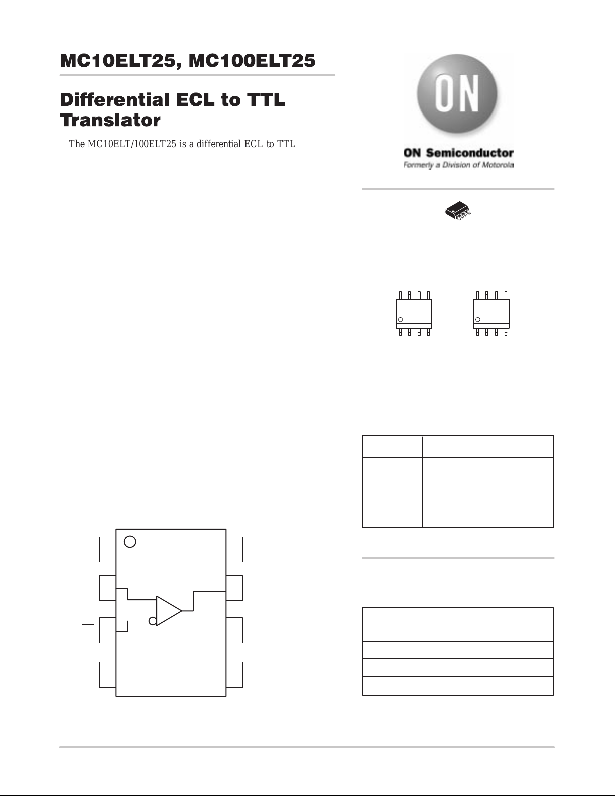
LOGIC DIAGRAM AND PINOUT ASSIGNMENT
input for a
EE
http://onsemi.com
8
1
SO–8
D SUFFIX
CASE 751
MARKING DIAGRAM
8
HLT25
ALYW
1
H = MC10
K = MC100
A = Assembly Location
*For additional information, see Application Note
AND8002/D
PIN DESCRIPTION
PIN FUNCTION
D Diff ECL Inputs
Q TTL Output
V
CC
V
EE
V
BB
GND Ground
Positive Supply
Negative Supply
Reference Output
8
KLT25
ALYW
1
L = Wafer Lot
Y = Year
W = Work Week
1
V
EE
2
D0
ECL
3
V
Semiconductor Components Industries, LLC, 1999
February , 2000 – Rev. 3
45
BB
TTL
V
78Q0
6
NCD0
GND
CC
ORDERING INFORMATION
Device Package Shipping
MC10EL T25D SO–8 98 Units / Rail
MC10EL T25DR2 SO–8
MC100EL T25D SO–8 98 Units / Rail
MC100EL T25DR2 SO–8
1 Publication Order Number:
2500 Units / Reel
2500 Units / Reel
MC10ELT25/D
Page 2
MC10ELT25, MC100ELT25
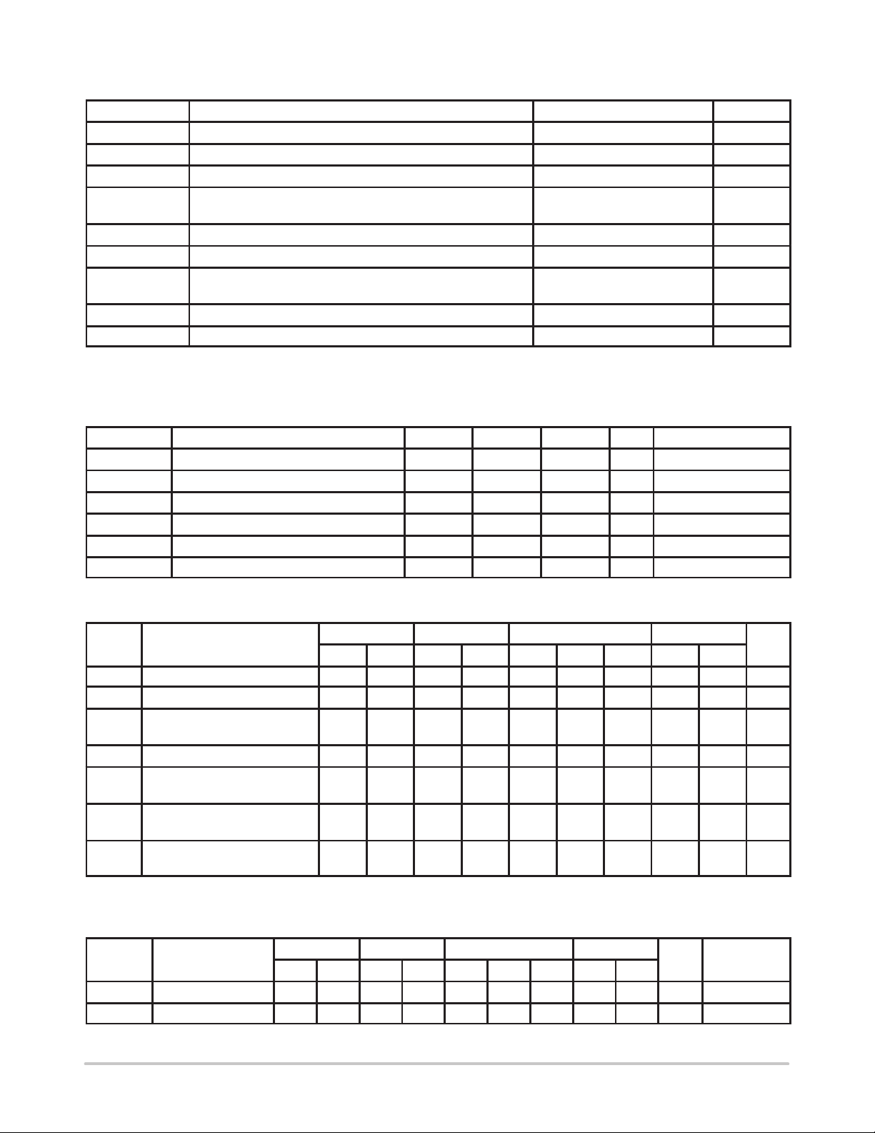
MAXIMUM RATINGS*
Symbol Parameter Value Unit
V
CC
V
EE
V
IN
I
OUT
T
A
T
STG
θ
JA
θ
JC
T
sol
* Maximum Ratings are those values beyond which damage to the device may occur. Functional operation should be restricted to the
Recommended Operating Conditions.
TTL OUTPUT DC CHARACTERISTICS
(VCC = 4.5V to 5.5V; VEE = –4.2V to –5.5V 100EL T, –4.94V to –5.5V 10ELT; TA = –40°C to 85°C)
Symbol Characteristic Min Typ Max Unit Condition
V
OH
V
OL
I
CCH
I
CCL
I
EE
I
OS
ECL INPUT DC CHARACTERISTICS
(VCC = 4.5V to 5.5V; VEE = –4.2V to –5.5V 100EL T, –4.94V to –5.5V 10ELT; TA = –40°C to 85°C)
Symbol Characteristic Min Max Min Max Min Typ Max Min Max Unit
I
IH
I
IL
V
CMR
V
PP
V
IH
V
IL
V
BB
1. 200mV input guarantees full logic swing at the output.
Input HIGH Current 150 150 150 150 µA
Input LOW Current 0.5 0.5 0.5 0.5 µA
Common Mode Range VEE +
Minimum Peak-to-Peak Input
Input HIGH Voltage 10ELT
Input LOW Voltage 10EL T
Reference Output 10ELT
DC Supply Voltage (Referenced to GND, VEE = –5.2) 7.0 V
DC Supply Voltage (Referenced to GND, VCC = 5.0) –8.0 V
Input Voltage 0 to V
Current Applied to Output in Low Output State Continuous
Operating Temperature Range (In Free-Air) –40 to 85 °C
Storage Temperature Range –55 to +150 °C
Thermal Resistance (Junction–to–Ambient) Still Air
Thermal Resistance (Junction–to–Case) 41 to 44 ± 5% °C/W
Solder Temperature (<2 to 3 Seconds: 245°C desired) 265 °C
Output HIGH Voltage 2.4 V IOH = –3.0mA
Output LOW Voltage 0.5 V IOL = 24mA
Power Supply Current 11 16 mA
Power Supply Current 13 18 mA
Power Supply Current 15 21 mA
Output Short Circuit Current –150 –60 mA
–40°C 0°C 25°C 85°C
1
100EL T
100EL T
100EL T
V
2.2
200 200 200 200 mV
–1230
–1165
–1950
–1810
–1.43
–1.38
CCVEE
–890
–880
–1500
–1475
–1.30
–1.26
+
2.2
–1170
–1165
–1950
–1810
–1.38
–1.38
Surge
500lfpm
V
CCVEE
–840
–880
–1480
–1475
–1.27
–1.26
+
2.2
–1130
–1165
–1950
–1810
–1.35
–1.38
CC
50
100
190
130
V
CCVEE
–810
–880
–1480
–1475
–1.25
–1.26
2.2
–1060
–1165
–1950
–1810
–1.31
–1.38
+
V
CC
–720
–880
–1445
–1475
–1.19
–1.26
V
mA
°C/W
V
mV
mV
V
AC CHARACTERISTICS
(VCC = 4.5V to 5.5V; VEE = –4.2V to –5.5V 100EL T, –4.94V to –5.5V 10ELT; TA = –40°C to 85°C)
–40°C 0°C 25°C 85°C
Symbol Characteristic Min Max Min Max Min Typ Max Min Max Unit Condition
t
PLH
t
PHL
Propagation Delay 1.7 3.6 1.7 3.6 1.7 3.6 1.7 3.6 ns CL = 20pF
Propagation Delay 2.6 4.1 2.6 4.1 2.6 4.1 2.6 4.1 ns CL = 20pF
http://onsemi.com
2
Page 3

MC10ELT25, MC100ELT25
P ACKAGE DIMENSIONS
SO–8
D SUFFIX
CASE 751–05
ISSUE P
–T–
–B–
–A–
M
B
58
1
4
M
4X P
J
_
X 45
R
0.25 (0.010)
_
M
G
F
C
SEATING
K
8X D
PLANE
SS
A0.25 (0.010)MTB
NOTES:
1. DIMENSIONS A AND B ARE DATUMS AND T IS A
DATUM SURFACE.
2. DIMENSIONING AND TOLERANCING PER ANSI
Y14.5M, 1982.
3. DIMENSIONS ARE IN MILLIMETER.
4. DIMENSION A AND B DO NOT INCLUDE MOLD
PROTRUSION.
5. MAXIMUM MOLD PROTRUSION 0.15 PER SIDE.
6. DIMENSION D DOES NOT INCLUDE MOLD
PROTRUSION. ALLOWABLE DAMBAR
PROTRUSION SHALL BE 0.127 TOTAL IN EXCESS
OF THE D DIMENSION AT MAXIMUM MATERIAL
CONDITION.
MILLIMETERS
DIM MIN MAX
A 4.80 5.00
B 3.80 4.00
C 1.35 1.75
D 0.35 0.49
F 0.40 1.25
G 1.27 BSC
J 0.18 0.25
K 0.10 0.25
M 0 7
P 5.80 6.20
R 0.25 0.50
__
http://onsemi.com
3
Page 4

MC10ELT25, MC100ELT25
ON Semiconductor and are trademarks of Semiconductor Components Industries, LLC (SCILLC). SCILLC reserves the right to make changes
without further notice to any products herein. SCILLC makes no warranty , representation or guarantee regarding the suitability of its products for any particular
purpose, nor does SCILLC assume any liability arising out of the application or use of any product or circuit, and specifically disclaims any and all liability ,
including without limitation special, consequential or incidental damages. “Typical” parameters which may be provided in SCILLC data sheets and/or
specifications can and do vary in different applications and actual performance may vary over time. All operating parameters, including “Typicals” must be
validated for each customer application by customer’s technical experts. SCILLC does not convey any license under its patent rights nor the rights of others.
SCILLC products are not designed, intended, or authorized for use as components in systems intended for surgical implant into the body, or other applications
intended to support or sustain life, or for any other application in which the failure of the SCILLC product could create a situation where personal injury or
death may occur. Should Buyer purchase or use SCILLC products for any such unintended or unauthorized application, Buyer shall indemnify and hold
SCILLC and its officers, employees, subsidiaries, affiliates, and distributors harmless against all claims, costs, damages, and expenses, and reasonable
attorney fees arising out of, directly or indirectly , any claim of personal injury or death associated with such unintended or unauthorized use, even if such claim
alleges that SCILLC was negligent regarding the design or manufacture of the part. SCILLC is an Equal Opportunity/Affirmative Action Employer .
PUBLICATION ORDERING INFORMATION
NORTH AMERICA Literature Fulfillment:
Literature Distribution Center for ON Semiconductor
P.O. Box 5163, Denver, Colorado 80217 USA
Phone: 303–675–2175 or 800–344–3860 Toll Free USA/Canada
Fax: 303–675–2176 or 800–344–3867 Toll Free USA/Canada
Email: ONlit@hibbertco.com
Fax Response Line: 303–675–2167 or 800–344–3810 T oll Free USA/Canada
N. American Technical Support: 800–282–9855 Toll Free USA/Canada
EUROPE: LDC for ON Semiconductor – European Support
German Phone: (+1) 303–308–7140 (M–F 1:00pm to 5:00pm Munich T ime)
Email: ONlit–german@hibbertco.com
French Phone: (+1) 303–308–7141 (M–F 1:00pm to 5:00pm T oulouse Time)
Email: ONlit–french@hibbertco.com
English Phone: (+1) 303–308–7142 (M–F 12:00pm to 5:00pm UK Time)
Email: ONlit@hibbertco.com
EUROPEAN TOLL–FREE ACCESS*: 00–800–4422–3781
*Available from Germany, France, Italy, England, Ireland
CENTRAL/SOUTH AMERICA:
Spanish Phone: 303–308–7143 (Mon–Fri 8:00am to 5:00pm MST)
Email: ONlit–spanish@hibbertco.com
ASIA/PACIFIC : LDC for ON Semiconductor – Asia Support
Phone: 303–675–2121 (Tue–Fri 9:00am to 1:00pm, Hong Kong Time)
T oll Free from Hong Kong & Singapore:
001–800–4422–3781
Email: ONlit–asia@hibbertco.com
JAPAN: ON Semiconductor, Japan Customer Focus Center
4–32–1 Nishi–Gotanda, Shinagawa–ku, T okyo, Japan 141–8549
Phone: 81–3–5740–2745
Email: r14525@onsemi.com
ON Semiconductor Website: http://onsemi.com
For additional information, please contact your local
Sales Representative.
http://onsemi.com
4
MC10EL T25/D
 Loading...