

Page 1

MOTOROLA
SEMICONDUCTOR TECHNICAL DATA
Low V oltage 2:8 Dif fer ential
Fanout Buffer
MC100L VE310
MC100E310
ECL/PECL Compatible
The MC100LVE310 is a low voltage, low skew 2:8 differential ECL
fanout buffer designed with clock distribution in mind. The device features
fully differential clock paths to minimize both device and system skew.
The LVE310 offers two selectable clock inputs to allow for redundant or
test clocks to be incorporated into the system clock trees. The
MC100E310 is pin compatible to the National 100310 device. The
MC100LVE310 works from a –3.3V supply while the MC100E310
provides identical function and performance from a standard –4.5V 100E
voltage supply.
• Dual Differential Fanout Buffers
• 200ps Part–to–Part Skew
• 50ps Output–to–Output Skew
• Low Voltage ECL/PECL Compatible
• 28–lead PLCC Packaging
For applications which require a single–ended input, the VBB reference
voltage is supplied. For single–ended input applications the V
reference should be connected to the CLK input and bypassed to ground
via a 0.01µf capacitor. The input signal is then driven into the CLK input.
To ensure that the tight skew specification is met it is necessary that
both sides of the differential output are terminated into 50Ω, even if only
one side is being used. In most applications all nine differential pairs will
be used and therefore terminated. In the case where fewer than nine
pairs are used it is necessary to terminate at least the output pairs
adjacent to the output pair being used in order to maintain minimum skew.
Failure to follow this guideline will result in small degradations of
propagation delay (on the order of 10–20ps) of the outputs being used,
while not catastrophic to most designs this will result in an increase in
skew. Note that the package corners isolate outputs from one another
such that the guideline expressed above holds only for outputs on the
same side of the package.
The MC100L VE310, as with most ECL devices, can be operated from a positive VCC supply in PECL mode. This allows the
LVE310 to be used for high performance clock distribution in +3.3V systems. Designers can take advantage of the LVE310’s
performance to distribute low skew clocks across the backplane or the board. In a PECL environment series or Thevenin line
terminations are typically used as they require no additional power supplies, if parallel termination is desired a terminating voltage
of VCC–2.0V will need to be provided. For more information on using PECL, designers should refer to Motorola Application Note
AN1406/D.
BB
LOW VOLTAGE
2:8 DIFFERENTIAL
FANOUT BUFFER
FN SUFFIX
PLASTIC PACKAGE
CASE 776–02
7/95
Motorola, Inc. 1996
4–1
REV 0.1
Page 2
MC100LVE310 MC100E310
V
EE
CLK_SEL
CLKa
V
CC
CLKa
V
BB
CLKb
Q0 Q0 Q1 V
25 24 23 22 21 20 19
26
27
28
1
2
3
4
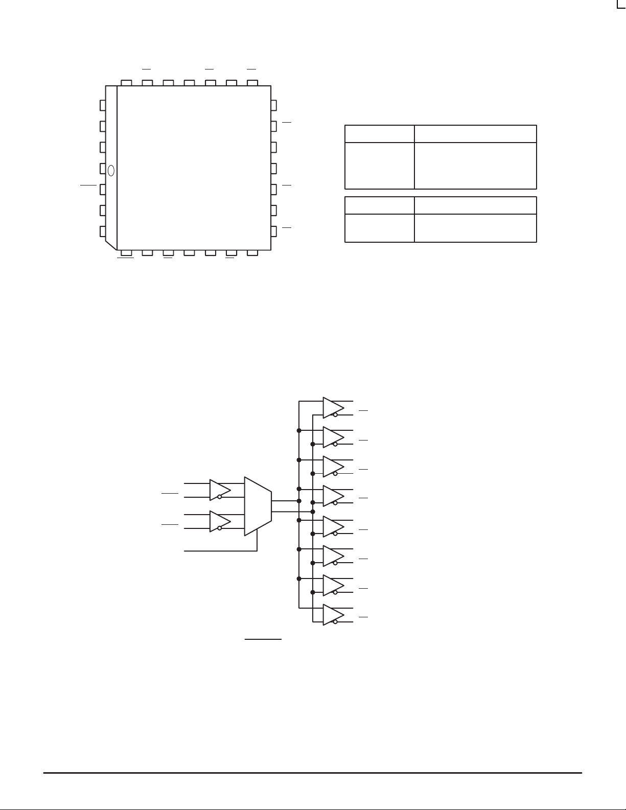
Pinout: 28–Lead PLCC
(Top View)
567891011
CLKb Q7 Q6NC V
CCO
CCO
Q1 Q2 Q2
Q7 Q6
18
17
16
15
14
13
12
Q3
Q3
Q4
V
Q4
Q5
Q5
CCO
PIN NAMES
Pins
CLKa, CLKb
Q0:7
V
BB
CLK_SEL
CLK_SEL
0
1
Function
Differential Input Pairs
Differential Outputs
VBB Output
Input Clock Select
Input Clock
CLKa Selected
CLKb Selected
CLKa
CLKa
CLKb
CLKb
CLK_SEL
LOGIC SYMBOL
Q0
Q0
Q1
Q1
Q2
Q2
Q3
Q3
Q4
Q4
Q5
Q5
Q6
Q6
Q7
Q7
V
BB
MOTOROLA ECLinPS and ECLinPS Lite
4–2
DL140 — Rev 3
Page 3

MC100LVE310 MC100E310
MC100L VE310
ECL DC CHARACTERISTICS
–40°C 0°C 25°C 85°C
Symbol Characteristic Min Typ Max Min Typ Max Min Typ Max Min Typ Max Unit
V
OH
V
OL
V
IH
V
IL
V
BB
V
EE
I
IH
I
EE
MC100L VE310
PECL DC CHARACTERISTICS
Symbol Characteristic Min Typ Max Min Typ Max Min Typ Max Min Typ Max Unit
V
OH
V
OL
V
IH
V
IL
V
BB
V
CC
I
IH
I
EE
1. These values are for VCC = 3.3V. Level Specifications will vary 1:1 with VCC.
Output HIGH Voltage –1.085 –1.005 –0.880 –1.025 –0.955 –0.880 –1.025 –0.955 –0.880 –1.025 –0.955 –0.880 V
Output LOW Voltage –1.830 –1.695 –1.555 –1.810 –1.705 –1.620 –1.810 –1.705 –1.620 –1.810 –1.705 –1.620 V
Input HIGH Voltage –1.165 –0.880 –1.165 –0.880 –1.165 –0.880 –1.165 –0.880 V
Input LOW Voltage –1.810 –1.475 –1.810 –1.475 –1.810 –1.475 –1.810 –1.475 V
Output Reference
Voltage
Power Supply Voltage –3.0 –3.8 –3.0 –3.8 –3.0 –3.8 –3.0 –3.8 V
Input HIGH Current 150 150 150 150 µA
Power Supply Current 55 60 55 60 55 60 65 70 mA
Output HIGH Voltage
Output LOW Voltage
Input HIGH Voltage
Input LOW Voltage
Output Reference
1
Voltage
Power Supply Voltage 3.0 3.8 3.0 3.8 3.0 3.8 3.0 3.8 V
Input HIGH Current 150 150 150 150 µA
Power Supply Current 55 60 55 60 55 60 65 70 mA
–1.38 –1.26 –1.38 –1.26 –1.38 –1.26 –1.38 –1.26 V
–40°C 0°C 25°C 85°C
1
2.215 2.295 2.42 2.275 2.345 2.420 2.275 2.345 2.420 2.275 2.345 2.420 V
1
1.47 1.605 1.745 1.490 1.595 1.680 1.490 1.595 1.680 1.490 1.595 1.680 V
1
2.135 2.420 2.135 2.420 2.135 2.420 2.135 2.420 V
1
1.490 1.825 1.490 1.825 1.490 1.825 1.490 1.825 V
1.92 2.04 1.92 2.04 1.92 2.04 1.92 2.04 V
MC100LVE310
AC CHARACTERISTICS (VEE = VEE (min) to VEE (max); VCC = V
–40°C 0°C 25°C 85°C
Symbol Characteristic Min Typ Max Min Typ Max Min Typ Max Min Typ Max Unit Condition
t
PLH
t
PHL
t
skew
V
PP
V
CMR
tr/t
1. The differential propagation delay is defined as the delay from the crossing points of the differential input signals to the crossing point of the
2. The single-ended propagation delay is defined as the delay from the 50% point of the input signal to the 50% point of the output signal. See
3. The within–device skew is defined as the worst case difference between any two similar delay paths within a single device.
4. VPP(min) is defined as the minimum input differential voltage which will cause no increase in the propagation delay . The VPP(min) is AC limited
5. V
Propagation Delay to Output
IN (differential)
IN (single–ended)
Within–Device Skew
Part–to–Part Skew (Diff)
Minimum Input Swing 500 500 500 500 mV Note 4
Common Mode Range –1.5 –0.4 –1.5 –0.4 –1.5 –0.4 –1.5 –0.4 V Note 5
Output Rise/Fall Time 200 600 200 600 200 600 200 600 ps 20%–80%
f
differential output signals. See
525
500
725
750
75
250
550
525
750
775
75
200
Definitions and T esting of ECLinPS AC Parameters
ECL Data Book (DL140/D).
Definitions and T esting of ECLinPS AC Parameters
in Chapter 1 (page 1–12) of the Motorola High Performance ECL Data Book (DL140/D).
for the LVE310 as a differential input as low as 50 mV will still produce full ECL levels at the output.
is defined as the range within which the VIH level may vary, with the device still meeting the propagation delay specification. The VIL level
CMR
must be such that the peak to peak voltage is less than 1.0 V and greater than or equal to VPP(min).
= GND)
CCO
550
550
750
800
50
200
575
600
775
850
50
200
ps
ps Note 3
in Chapter 1 (page 1–12) of the Motorola High Performance
Note 1
Note 2
DL140 — Rev 3
4–3 MOTOROLAECLinPS and ECLinPS Lite
Page 4

MC100LVE310 MC100E310
MC100E310
ECL DC CHARACTERISTICS
–40°C 0°C 25°C 85°C
Symbol Characteristic Min Typ Max Min Typ Max Min Typ Max Min Typ Max Unit
V
OH
V
OL
V
IH
V
IL
V
BB
V
EE
I
IH
I
EE
MC100E310
PECL DC CHARACTERISTICS
Symbol Characteristic Min Typ Max Min Typ Max Min Typ Max Min Typ Max Unit
V
OH
V
OL
V
IH
V
IL
V
BB
V
CC
I
IH
I
EE
1. These values are for VCC = 5.0V. Level Specifications will vary 1:1 with VCC.
Output HIGH Voltage –1.085 –1.005 –0.880 –1.025 –0.955 –0.880 –1.025 –0.955 –0.880 –1.025 –0.955 –0.880 V
Output LOW Voltage –1.830 –1.695 –1.555 –1.810 –1.705 –1.620 –1.810 –1.705 –1.620 –1.810 –1.705 –1.620 V
Input HIGH Voltage –1.165 –0.880 –1.165 –0.880 –1.165 –0.880 –1.165 –0.880 V
Input LOW Voltage –1.810 –1.475 –1.810 –1.475 –1.810 –1.475 –1.810 –1.475 V
Output Reference
Voltage
Power Supply Voltage –5.25 –4.2 –5.25 –4.2 –5.25 –4.2 –5.25 –4.2 V
Input HIGH Current 150 150 150 150 µA
Power Supply Current 55 60 55 60 55 60 65 70 mA
Output HIGH Voltage13.915 3.995 4.12 3.975 4.045 4.12 3.975 4.045 4.12 3.975 4.045 4.12 V
Output LOW Voltage13.170 3.305 3.445 3.19 3.295 3.38 3.19 3.295 3.38 3.19 3.295 3.38 V
Input HIGH Voltage
Input LOW Voltage
Output Reference
1
Voltage
Power Supply Voltage 4.75 5.25 4.75 5.25 4.75 5.25 4.75 5.25 V
Input HIGH Current 150 150 150 150 µA
Power Supply Current 55 60 55 60 55 60 65 70 mA
–1.38 –1.26 –1.38 –1.26 –1.38 –1.26 –1.38 –1.26 V
–40°C 0°C 25°C 85°C
1
3.835 4.12 3.835 4.12 3.835 4.12 3.835 4.12 V
1
3.190 3.525 3.190 3.525 3.190 3.525 3.190 3.525 V
3.62 3.74 3.62 3.74 3.62 3.74 3.62 3.74 V
MC100E310
AC CHARACTERISTICS (VEE = VEE (min) to VEE (max); VCC = V
–40°C 0°C 25°C 85°C
Symbol Characteristic Min Typ Max Min Typ Max Min Typ Max Min Typ Max Unit Condition
t
PLH
t
PHL
t
skew
V
PP
V
CMR
tr/t
1. The differential propagation delay is defined as the delay from the crossing points of the differential input signals to the crossing point of the
2. The single-ended propagation delay is defined as the delay from the 50% point of the input signal to the 50% point of the output signal. See
3. The within–device skew is defined as the worst case difference between any two similar delay paths within a single device.
4. VPP(min) is defined as the minimum input differential voltage which will cause no increase in the propagation delay . The VPP(min) is AC limited
5. V
Propagation Delay to Output
IN (differential)
IN (single–ended)
Within–Device Skew
Part–to–Part Skew (Diff)
Minimum Input Swing 500 500 500 500 mV Note 4
Common Mode Range –1.5 –0.4 –1.5 –0.4 –1.5 –0.4 –1.5 –0.4 V note 5
Output Rise/Fall Time 200 600 200 600 200 600 200 600 ps 20%–80%
f
differential output signals. See
525
500
725
750
75
250
550
525
750
775
75
200
Definitions and T esting of ECLinPS AC Parameters
ECL Data Book (DL140/D).
Definitions and T esting of ECLinPS AC Parameters
in Chapter 1 (page 1–12) of the Motorola High Performance ECL Data Book (DL140/D).
for the E310 as a differential input as low as 50 mV will still produce full ECL levels at the output.
is defined as the range within which the VIH level may vary, with the device still meeting the propagation delay specification. The VIL level
CMR
must be such that the peak to peak voltage is less than 1.0 V and greater than or equal to VPP(min).
= GND)
CCO
550
550
750
800
50
200
575
600
775
850
50
200
ps
ps Note 3
in Chapter 1 (page 1–12) of the Motorola High Performance
Note 1
Note 2
MOTOROLA ECLinPS and ECLinPS Lite
4–4
DL140 — Rev 3
Page 5

-L-
28 1
-N-
MC100LVE310 MC100E310
OUTLINE DIMENSIONS
FN SUFFIX
PLASTIC PLCC PACKAGE
CASE 776–02
ISSUE D
SNSM
0.007 (0.180) T L
Y BRK
B
0.007 (0.180) T L
U
D
Z
-M-
D
W
V
X
VIEW D-D
–M
G1
0.010 (0.250) T L
–M
SNSM
SNSS
–M
Z
C
G
G1
0.010 (0.250) T L
0.007 (0.180) T L
A
0.007 (0.180) T L
R
E
0.004 (0.100)
SEATING
-T-
J
PLANE
VIEW S
SNSS
–M
NOTES:
1. DATUMS -L-, -M-, AND -N- DETERMINED
WHERE TOP OF LEAD SHOULDER EXITS
PLASTIC BODY AT MOLD PARTING LINE.
2. DIM G1, TRUE POSITION TO BE MEASURED
AT DATUM -T-, SEATING PLANE.
3. DIM R AND U DO NOT INCLUDE MOLD FLASH.
ALLOWABLE MOLD FLASH IS 0.010 (0.250)
PER SIDE.
4. DIMENSIONING AND TOLERANCING PER ANSI
Y14.5M, 1982.
5. CONTROLLING DIMENSION: INCH.
6. THE PACKAGE TOP MAY BE SMALLER THAN
THE PACKAGE BOTTOM BY UP TO 0.012
(0.300). DIMENSIONS R AND U ARE
DETERMINED AT THE OUTERMOST
EXTREMES OF THE PLASTIC BODY
EXCLUSIVE OF MOLD FLASH, TIE BAR
BURRS, GATE BURRS AND INTERLEAD
FLASH, BUT INCLUDING ANY MISMATCH
BETWEEN THE TOP AND BOTTOM OF THE
PLASTIC BODY.
7. DIMENSION H DOES NOT INCLUDE DAMBAR
PROTRUSION OR INTRUSION. THE DAMBAR
PROTRUSION(S) SHALL NOT CAUSE THE H
DIMENSION TO BE GREATER THAN 0.037
(0.940). THE DAMBAR INTRUSION(S) SHALL
NOT CAUSE THE H DIMENSION TO BE
SMALLER THAN 0.025 (0.635).
–M
–M
SNSM
SNSM
H
0.007 (0.180) T L
–M
SNSM
K1
K
SNSM
0.007 (0.180) T L
F
–M
VIEW S
INCHES MILLIMETERS
MIN MINMAX MAX
DIM
A
0.485
B
0.485
C
0.165
E
0.090
F
0.013
G
0.050 BSC
H
0.026
J
0.020
K
0.025
R
0.450
U
0.450
V
0.042
W
0.042
X
0.042
Y
—
Z
2°
G1
0.410
K1
0.040
0.495
0.495
0.180
0.110
0.019
0.032
0.456
0.456
0.048
0.048
0.056
0.020
10°
0.430
12.32
12.57
12.32
12.57
4.20
4.57
2.29
2.79
0.33
0.48
1.27 BSC
0.66
0.81
0.51
0.64
11.43
11.43
1.07
1.07
1.07
10.42
1.02
—
—
11.58
11.58
1.21
1.21
1.42
—
0.50
2°
10°
10.92
—
—
—
—
DL140 — Rev 3
4–5 MOTOROLAECLinPS and ECLinPS Lite
Page 6

MC100LVE310 MC100E310
Motorola reserves the right to make changes without further notice to any products herein. Motorola makes no warranty , representation or guarantee regarding
the suitability of its products for any particular purpose, nor does Motorola assume any liability arising out of the application or use of any product or circuit, and
specifically disclaims any and all liability, including without limitation consequential or incidental damages. “T ypical” parameters which may be provided in Motorola
data sheets and/or specifications can and do vary in different applications and actual performance may vary over time. All operating parameters, including “Typicals”
must be validated for each customer application by customer’s technical experts. Motorola does not convey any license under its patent rights nor the rights of
others. Motorola products are not designed, intended, or authorized for use as components in systems intended for surgical implant into the body, or other
applications intended to support or sustain life, or for any other application in which the failure of the Motorola product could create a situation where personal injury
or death may occur. Should Buyer purchase or use Motorola products for any such unintended or unauthorized application, Buyer shall indemnify and hold Motorola
and its officers, employees, subsidiaries, affiliates, and distributors harmless against all claims, costs, damages, and expenses, and reasonable attorney fees
arising out of, directly or indirectly, any claim of personal injury or death associated with such unintended or unauthorized use, even if such claim alleges that
Motorola was negligent regarding the design or manufacture of the part. Motorola and are registered trademarks of Motorola, Inc. Motorola, Inc. is an Equal
Opportunity/Affirmative Action Employer.
How to reach us:
USA/EUROPE/Locations Not Listed: Motorola Literature Distribution; JAPAN: Nippon Motorola Ltd.; Tatsumi–SPD–JLDC, 6F Seibu–Butsuryu–Center,
P.O. Box 20912; Phoenix, Arizona 85036. 1–800–441–2447 or 602–303–5454 3–14–2 Tatsumi Koto–Ku, Tokyo 135, Japan. 03–81–3521–8315
MFAX: RMF AX0@email.sps.mot.com – T OUCHTONE 602–244–6609 ASIA/PACIFIC: Motorola Semiconductors H.K. Ltd.; 8B Tai Ping Industrial Park,
INTERNET: http://Design–NET .com 51 Ting Kok Road, Tai Po, N.T., Hong Kong. 852–26629298
MOTOROLA ECLinPS and ECLinPS Lite
4–6
*MC100LVE310/D*
◊
MC100LVE310/D
DL140 — Rev 3
 Loading...