

Page 1
SEMICONDUCTOR TECHNICAL DATA
2–1
REV 2
Motorola, Inc. 1996
7/96
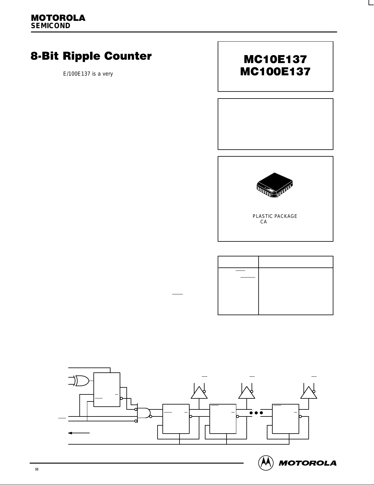
The MC10E/100E137 is a very high speed binary ripple counter. The
two least significant bits were designed with very fast edge rates while the
more significant bits maintain standard ECLinPS output edge rates.
This allows the counter to operate at very high frequencies while
maintaining a moderate power dissipation level.
• 1.8GHz Minimum Count Frequency
• Differential Clock Input and Data Output Pins
• V
BB
Output for Single-Ended Use
• Internal 75kΩ Input Pulldown Resistors
• Synchronous and Asynchronous Enable Pins
• Asynchronous Master Reset
• Extended 100E V
EE
Range of –4.2V to –5.46V
The device is ideally suited for multiple frequency clock generation as
well as a counter in a high performance ATE time measurement board.
Both asynchronous and synchronous enables are available to
maximize the device’s flexibility for various applications. The
asynchronous enable input, A_Start, when asserted enables the counter
while overriding any synchronous enable signals. The E137 features
XORed enable inputs, EN1 and EN2, which are synchronous to the CLK
input. When only one synchronous enable is asserted the counter
becomes disabled on the next CLK transition; all outputs remain in the
previous state poised for the other synchronous enable or A_Start to be
asserted to re-enable the counter. Asserting both synchronous enables
causes the counter to become enabled on the next transition of the CLK.
If EN1 (or EN2) and CLK edges are coincident, sufficient delay has been
inserted in the CLK path (to compensate for the XOR gate delay and the
internal D-flip flop setup time) to insure that the synchronous enable
signal is clocked correctly, hence, the counter is disabled.
The E137 can also be driven single-endedly utilizing the VBB output
supply as the voltage reference for the CLK input signal. If a single-ended
signal is to be used the VBB pin should be connected to the CLK
input and
bypassed to ground via a 0.01µF capacitor. VBB can only source/sink
0.5mA, therefore it should be used as a switching reference for the E137
only.
All input pins left open will be pulled LOW via an input pulldown resistor. Therefore, do not leave the differential CLK inputs
open. Doing so causes the current source transistor of the input clock gate to become saturated, thus upsetting the internal bias
regulators and jeopardizing the stability of the device.
The asynchronous Master Reset resets the counter to an all zero state upon assertion.
CLK
CLK
LOGIC DIAGRAM
Q
Q
CLK
CLK
D
R
Q
Q
CLK
CLK
D
R
EN1
EN2
CLK
CLK
A_Start
Q
Q
D
R
Q0 Q0 Q1 Q1
Q
Q
CLK
CLK
D
R
Q7 Q7
MR
V
BB
8-BIT RIPPLE
COUNTER
FN SUFFIX
PLASTIC PACKAGE
CASE 776-02
CLK, CLK
Q0-Q7, Q0-Q7
A_Start
EN1, EN2
MR
V
BB
Differential Clock Inputs
Differential Q Outputs
Asynchronous Enable Input
Synchronous Enable Inputs
Asynchronous Master Reset
Switching Refernce Output
PIN FUNCTION
PIN NAMES
Page 2

MC10E137 MC100E137
MOTOROLA ECLinPS and ECLinPS Lite
DL140 — Rev 4
2–2
V
CCO
1
Q0
Q7 Q7 Q6 Q6 Q5 Q5
Q4
Q4
V
CC
Q3
Q3
Q2
Q2
V
CCO
Q1Q1Q0
V
CCO
MR
V
BB
CLK
CLK
V
EE
EN2
EN1
A_Start
4
3
2
28
27
26
25
24
23
22
21
20
19
18
17
16
15
14
13
12
11109
7
8
6
5
Pinout: 28-Lead PLCC (Top View)
* All VCC and V
CCO
pins are tied together on the die.
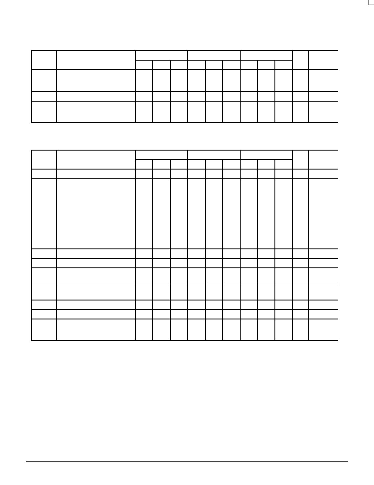
SEQUENTIAL TRUTH TABLE
Function EN1 EN2 A_Start MR CLK Q7 Q6 Q5 Q4 Q3 Q2 Q1 Q0
Reset X X X H X L L L L L L L L
Count L
L
L
L
L
L
L
L
L
L
L
L
Z
Z
Z
L
L
L
L
L
L
L
L
L
L
L
L
L
L
L
L
L
L
L
H
H
H
L
H
Stop H
H
L
L
L
L
L
L
Z
Z
L
L
L
L
L
L
L
L
L
L
L
L
H
H
H
H
Asynch Start H
H
L
L
L
L
H
H
H
L
L
L
Z
Z
Z
L
L
L
L
L
L
L
L
L
L
L
L
L
L
L
H
H
H
L
L
H
L
H
L
Count L
L
L
L
L
L
L
L
L
L
L
L
Z
Z
Z
L
L
L
L
L
L
L
L
L
L
L
L
L
H
H
H
L
L
H
L
L
H
L
H
Stop L
L
H
H
L
L
L
L
Z
Z
L
L
L
L
L
L
L
L
H
H
L
L
L
L
H
H
Synch Start H
H
H
H
H
H
L
L
L
L
L
L
Z
Z
Z
L
L
L
L
L
L
L
L
L
L
L
L
H
H
H
L
L
H
H
H
L
L
H
L
Stop H
H
L
L
L
L
L
L
Z
Z
L
L
L
L
L
L
L
L
H
H
H
H
L
L
L
L
Count L
L
L
L
L
L
L
L
L
L
L
L
Z
Z
Z
L
L
L
L
L
L
L
L
L
L
L
L
H
H
H
H
H
H
L
H
H
H
L
H
Reset X X X H X L L L L L L L L
Z = Low to High Transition
Page 3
MC10E137 MC100E137
2–3 MOTOROLAECLinPS and ECLinPS Lite
DL140 — Rev 4
DC CHARACTERISTICS (VEE = VEE(min) to VEE(max); VCC = V
CCO
= GND)
0°C 25°C 85°C
Symbol Characteristic Min Typ Max Min Typ Max Min Typ Max Unit Condition
V
BB
Output Reference Voltage
10E
100E
–1.38
–1.38
–1.27
–1.27
–1.35
–1.38
–1.25
–1.26
–1.31
–1.38
–1.19
–1.26
V
I
IH
Input HIGH Current 150 150 150 µA
I
EE
Power Supply Current
10E
100E
121
121
145
145
121
121
145
145
121
139
145
167
mA
AC CHARACTERISTICS (VEE = VEE(min) to VEE(max); VCC = V
CCO
= GND)
0°C 25°C 85°C
Symbol Characteristic Min Typ Max Min Typ Max Min Typ Max Unit Condition
f
COUNT
Maximum Count Frequency 1800 2200 1800 2200 1800 2200 MHz
t
PLH
t
PHL
Propagation Delay to Output
CLK to Q0
CLK to Q1
CLK to Q2
CLK to Q3
CLK to Q4
CLK to Q5
CLK to Q6
CLK to Q7
A_Start to Q0
MR to Q0
1300
1600
1950
2275
2625
2950
3250
3575
950
700
1700
2025
2425
2750
3125
3450
3775
4075
1325
1000
2150
2500
2925
3350
3750
4150
4450
4800
1700
1300
1300
1600
1950
2275
2625
2950
3250
3575
950
700
1700
2050
2450
2775
3150
3475
3800
4125
1325
1000
2150
2500
2925
3350
3750
4150
4450
4800
1700
1300
1350
1650
2025
2350
2700
3050
3375
3700
950
700
1750
2100
2500
2850
3225
3550
3925
4250
1325
1000
2200
2550
3000
3425
3825
4250
4600
4950
1700
1300
ps
t
s
Setup Time (EN1, EN2) 0 –150 0 –150 0 –150 ps
t
h
Hold Time (EN1, EN2) 300 150 300 150 300 150 ps
t
RR
Reset Recovery Time
MR, A_Start
400 200 400 200 400 200
ps
t
PW
Minimum Pulse Width
CLK, MR, A_Start
400 400 400
ps
V
PP
Minimum Input Swing (CLK) 0.25 1.0 0.25 1.0 0.25 1.0 V Note 1
V
CMR
Com Mode Range (CLK) –0.4 –2.0 –0.4 –2.0 –0.4 –2.0 V
t
r
t
f
Rise/Fall Times
Q0,Q1
Q2 to Q7
150
275
400
600
150
275
400
600
150
275
400
600
ps 20%–80%
1. Minimum input swing for which AC parameters are guaranteed. Full DC ECL output swings will be generated with only 50mV input swings.
Page 4
MC10E137 MC100E137
MOTOROLA ECLinPS and ECLinPS Lite
DL140 — Rev 4
2–4
OUTLINE DIMENSIONS
FN SUFFIX
PLASTIC PLCC PACKAGE
CASE 776–02
ISSUE D
0.007 (0.180) T L
–M
SNSM
0.007 (0.180) T L
–M
SNSM
0.007 (0.180) T L
–M
SNSM
0.010 (0.250) T L
–M
SNSS
0.007 (0.180) T L
–M
SNSM
0.010 (0.250) T L
–M
SNSS
0.007 (0.180) T L
–M
SNSM
0.007 (0.180) T L
–M
SNSM
0.004 (0.100)
SEATING
PLANE
-T-
12.32
12.32
4.20
2.29
0.33
0.66
0.51
0.64
11.43
11.43
1.07
1.07
1.07
—
2
°
10.42
1.02
12.57
12.57
4.57
2.79
0.48
0.81
—
—
11.58
11.58
1.21
1.21
1.42
0.50
10
°
10.92
—
1.27 BSC
A
B
C
E
F
G
H
J
K
R
U
V
W
X
Y
Z
G1
K1
MIN MINMAX MAX
INCHES MILLIMETERS
DIM
NOTES:
1. DATUMS -L-, -M-, AND -N- DETERMINED
WHERE TOP OF LEAD SHOULDER EXITS
PLASTIC BODY AT MOLD PARTING LINE.
2. DIM G1, TRUE POSITION TO BE MEASURED
AT DATUM -T-, SEATING PLANE.
3. DIM R AND U DO NOT INCLUDE MOLD FLASH.
ALLOWABLE MOLD FLASH IS 0.010 (0.250)
PER SIDE.
4. DIMENSIONING AND TOLERANCING PER ANSI
Y14.5M, 1982.
5. CONTROLLING DIMENSION: INCH.
6. THE PACKAGE TOP MAY BE SMALLER THAN
THE PACKAGE BOTTOM BY UP TO 0.012
(0.300). DIMENSIONS R AND U ARE
DETERMINED AT THE OUTERMOST
EXTREMES OF THE PLASTIC BODY
EXCLUSIVE OF MOLD FLASH, TIE BAR
BURRS, GATE BURRS AND INTERLEAD
FLASH, BUT INCLUDING ANY MISMATCH
BETWEEN THE TOP AND BOTTOM OF THE
PLASTIC BODY.
7. DIMENSION H DOES NOT INCLUDE DAMBAR
PROTRUSION OR INTRUSION. THE DAMBAR
PROTRUSION(S) SHALL NOT CAUSE THE H
DIMENSION TO BE GREATER THAN 0.037
(0.940). THE DAMBAR INTRUSION(S) SHALL
NOT CAUSE THE H DIMENSION TO BE
SMALLER THAN 0.025 (0.635).
VIEW S
B
U
Z
G1
X
VIEW D-D
H
K
F
VIEW S
G
C
Z
A
R
E
J
0.485
0.485
0.165
0.090
0.013
0.026
0.020
0.025
0.450
0.450
0.042
0.042
0.042
—
2
°
0.410
0.040
0.495
0.495
0.180
0.110
0.019
0.032
—
—
0.456
0.456
0.048
0.048
0.056
0.020
10
°
0.430
—
0.050 BSC
-N-
Y BRK
D
D
W
-M-
-L-
28 1
V
G1
K1
Page 5

MC10E137 MC100E137
2–5 MOTOROLAECLinPS and ECLinPS Lite
DL140 — Rev 4
Motorola reserves the right to make changes without further notice to any products herein. Motorola makes no warranty , representation or guarantee regarding
the suitability of its products for any particular purpose, nor does Motorola assume any liability arising out of the application or use of any product or circuit, and
specifically disclaims any and all liability , including without limitation consequential or incidental damages. “Typical” parameters which may be provided in Motorola
data sheets and/or specifications can and do vary in different applications and actual performance may vary over time. All operating parameters, including “Typicals”
must be validated for each customer application by customer’s technical experts. Motorola does not convey any license under its patent rights nor the rights of
others. Motorola products are not designed, intended, or authorized for use as components in systems intended for surgical implant into the body, or other
applications intended to support or sustain life, or for any other application in which the failure of the Motorola product could create a situation where personal injury
or death may occur. Should Buyer purchase or use Motorola products for any such unintended or unauthorized application, Buyer shall indemnify and hold Motorola
and its officers, employees, subsidiaries, affiliates, and distributors harmless against all claims, costs, damages, and expenses, and reasonable attorney fees
arising out of, directly or indirectly, any claim of personal injury or death associated with such unintended or unauthorized use, even if such claim alleges that
Motorola was negligent regarding the design or manufacture of the part. Motorola and are registered trademarks of Motorola, Inc. Motorola, Inc. is an Equal
Opportunity/Affirmative Action Employer.
How to reach us:
USA/EUROPE/Locations Not Listed: Motorola Literature Distribution; JAPAN: Nippon Motorola Ltd.; Tatsumi–SPD–JLDC, 6F Seibu–Butsuryu–Center,
P.O. Box 20912; Phoenix, Arizona 85036. 1–800–441–2447 or 602–303–5454 3–14–2 Tatsumi Koto–Ku, Tokyo 135, Japan. 03–81–3521–8315
MFAX: RMFAX0@email.sps.mot.com – TOUCHTONE 602–244–6609 ASIA/PACIFIC: Motorola Semiconductors H.K. Ltd.; 8B Tai Ping Industrial Park,
INTERNET: http://Design–NET.com 51 Ting Kok Road, Tai Po, N.T., Hong Kong. 852–26629298
MC10E137/D
*MC10E137/D*
◊
 Loading...