

Page 1
Features
S
Guard Ring Die Construction for
·
Transient Protection
Low Power Loss, High Efficiency
·
Low Reverse Current
·
For Use in Low Voltage, High Frequency
·
Inverters, Free Wheeling, and Polarity
Protection Applications
Mechanical Data
Case: POWERMITEâ3, Molded Plastic
·
Plastic Material: UL Flammability
·
NEW PRODUCT
Classification Rating 94V-0
Moisture sensitivity: Level 1 per J-STD-020A
·
Terminals: Solderable per MIL-STD-202,
·
Method 208
Polarity: See Diagram
·
· Marking: See Page 3
· Weight: 0.072 grams (approx.)
· Ordering Information: See Page 3
MBRM360
3A SURFACE MOUNT SCHOTTKY BARRIER RECTIFIER
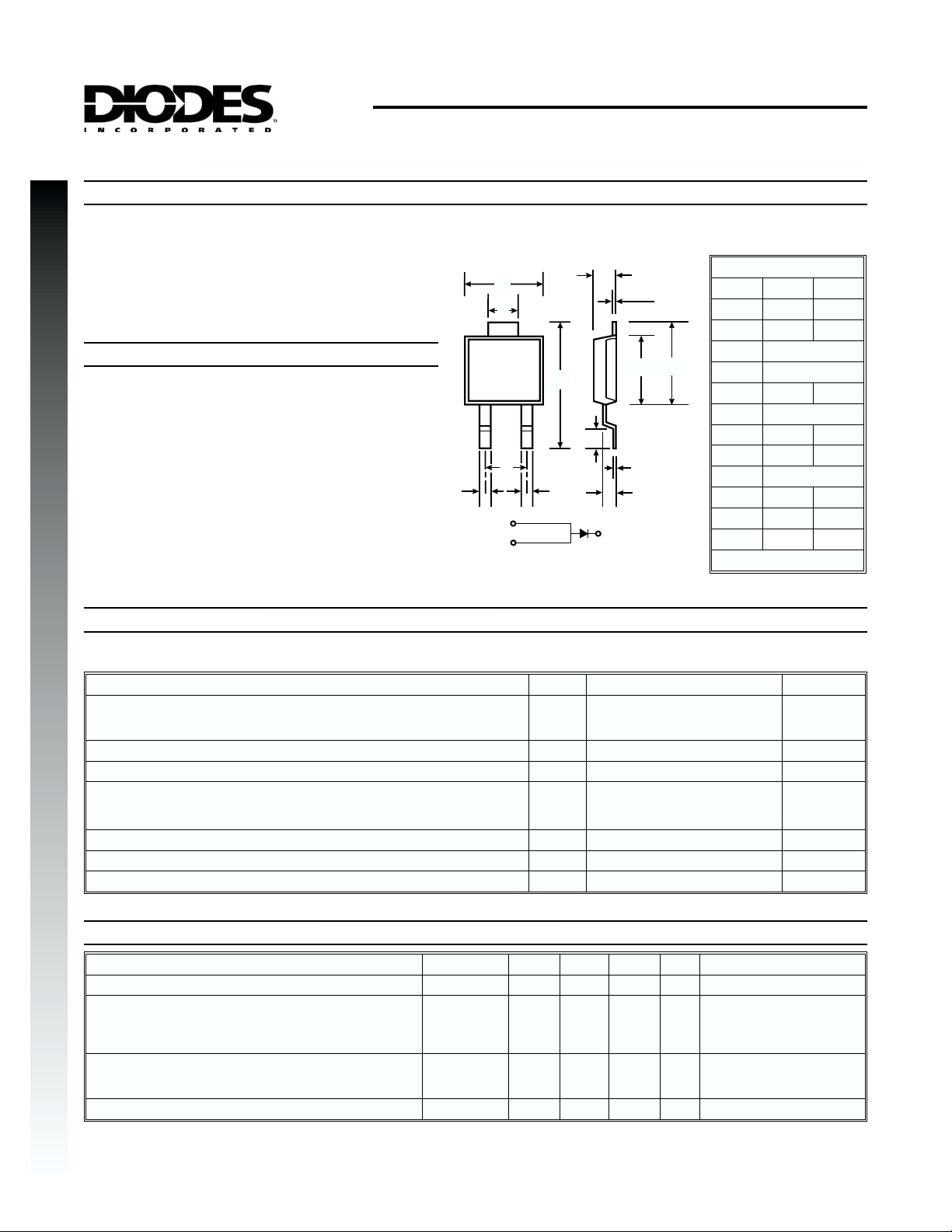
POWERMITEâ3
A
E
P
3
J
B
12
M
D
C
PIN 1
PIN 2
Note: Pins 1 & 2 must be electrically
connected at the printed circuit board.
C
K
L
PIN 3, BOTTOMSIDE
HEAT
INK
G
H
POWERMITEâ3
A
B
C
D
E
G
H
J
K
L
M
P
Min Max
4.03 4.09
6.40 6.61
.889 NOM
1.83 NOM
1.10 1.14
.178 NOM
5.01 5.17
4.37 4.43
.178 NOM
.71 .77
.36 .46
1.73 1.83
Dim
All Dimensions in mm
Maximum Ratings
Single phase, half wave, 60Hz, resistive or inductive load.
For capacitive load, derate current by 20%.
Peak Repetitive Reverse Voltage
Working Peak Reverse Voltage
DC Blocking Voltage
RMS Reverse Voltage
Average Rectified Output Current (See also Figure 5)
Non-Repetitive Peak Forward Surge Current
8.3ms Single half sine-wave superimposed on rated load @ T
(JEDEC Method) @ T
Typical Thermal Resistance Junction to Soldering Point
Operating Temperature Range
Storage Temperature Range
Electrical Characteristics
Characteristic Symbol
Reverse Breakdown Voltage (Note 1)
Forward Voltage (Note 1)
Reverse Current (Note 1)
Total Capacitance
@ TA= 25°C unless otherwise specified
Characteristic Symbol
@ TA= 25°C unless otherwise specified
= 25°C
C
= 100°C
C
V
(BR)R
V
FM
I
RM
C
Value
V
RRM
V
RWM
V
R
V
R(RMS)
I
O
I
FSM
R
qJS
T
j
T
STG
Min Typ Max Unit
60 ¾¾V
¾
0.59
¾
0.53
¾
0.72
¾
0.63
¾
¾
¾
T
¾ 130 ¾ pF
2.0
0.6
2.5
0.63
0.57
0.76
0.67
200
20
150
60 V
42 V
3A
100
50
3.2 °C/W
-55 to +125 °C
-55 to +150 °C
Test Condition
= 0.2mA
I
R
= 3A, Tj= 25°C
I
F
= 3A, Tj= 125°C
I
F
V
= 6A, Tj= 25°C
I
F
= 6A, Tj= 125°C
I
F
= 25°C, VR= 60V
mA
T
j
= 100°C, VR= 60V
T
mA
j
= 125°C, VR= 60V
T
mA
j
f = 1.0MHz, V
Unit
= 4.0V DC
R
A
Notes: 1. Short duration test pulse used to minimize self-heating effect.
DS30355 Rev. 2 - 2 1 of 3 MBRM360
Page 2
10,000
g
100
g
1.0
10
g
1000
g
0.1
T = +125ºC
j
T = +25ºC
j
T = +100ºC
j
m
T = +125 C
°
j
1000
°
T = +100 C
j
100
T = +75 C
°
j
10
NEW PRODUCT
0.01
F
I , INSTANTANEOUS FORWARD CURRENT (A)
80
60
40
20
FSM
I , PEAK FWD SURGE CURRENT (A)
0
1 10 100
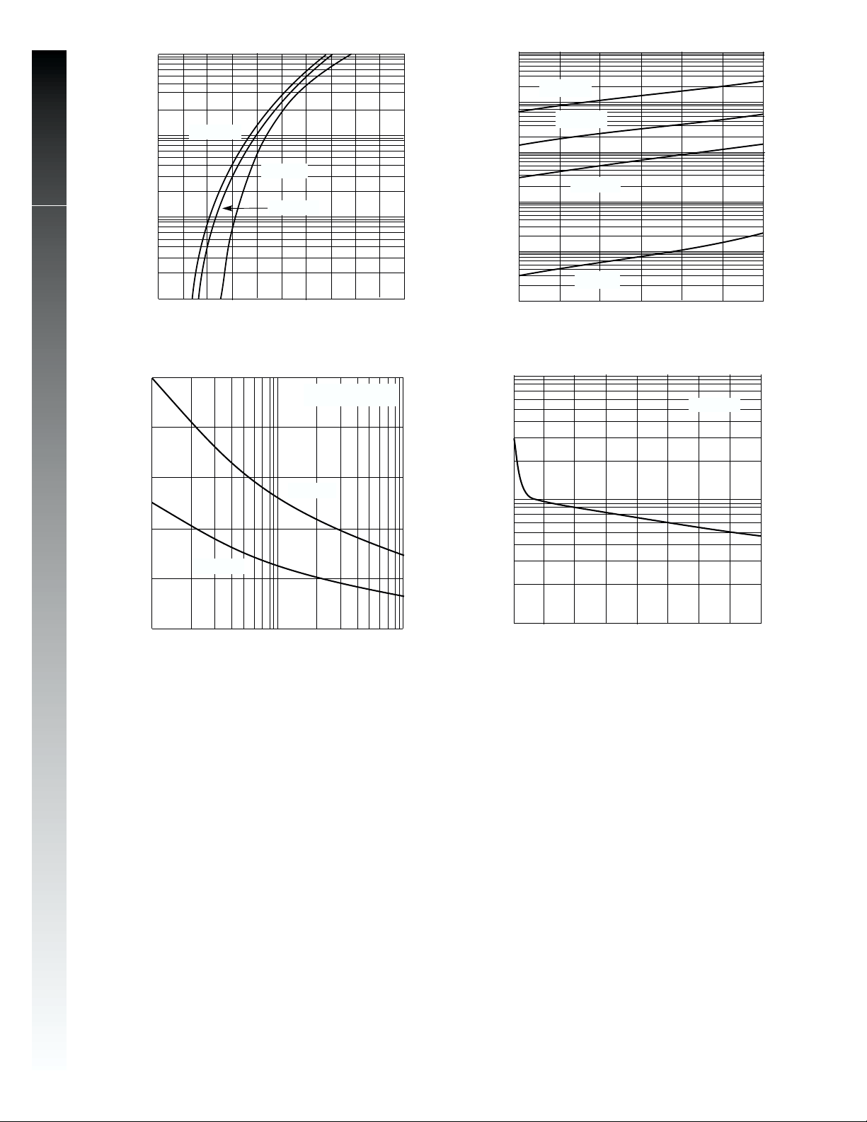
. 3 Max Non-Repetitive Peak Fwd Surge Current
Fi
0 0.2 0.4 0.6
V , INSTANTANEOUS FORWARD VOLTAGE (V)
F
Fi
.1 Typ. Forward Characteristics
T = +25ºC
C
T = +100ºC
C
0.8 1.0
Single Half-Sine-Wave
(JEDEC Method)
NUMBER OF CYCLES AT 60 Hz
R
I , INSTANTANEOUS REVERSE CURRENT ( A)
T
C , TOTAL CAPACITANCE (pF)
1
T = +25 Cj°
0.1
0
V , INSTANTANEOUS REVERSE VOLTAGE (V)
R
Fi
20
10
30
.2 Typical Reverse Characteristics
100
10
0
Fi
15
7.5
V , REVERSE VOLTAGE (V)
R
.4 Typical Capacitance vs. Reverse Voltage
22.5
30
37.5
40
f = 1MHz
45
50
52.5
60
60
DS30355 Rev. 2 - 2 2 of 3 MBRM360
Page 3
3.5
4
g
g
g
2.5
4
T = 125°C
3
2
Note 2
Note 3
j
3
2
Note 5
1.5
1
F
NEW PRODUCT
I , DC FORWARD CURRENT (A)
0.5
0
25
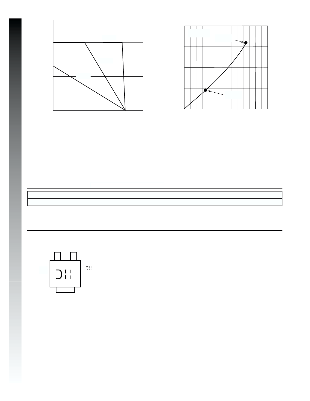
Notes: 2. TA= T
3. Device mounted on GETEK substrate, 2”x2”, 2 oz. copper, double-sided, cathode pad dimensions 0.75” x 1.0”, anode pad
dimensions 0.25” x 1.0”. R
4. Device mounted on FR-4 substrate, 2”x2”, 2 oz. copper, single-sided, pad layout as per Diodes Inc. suggested pad layout
document AP02001 which can be found on our website at http://www.diodes.com/datasheets/ap02001.pdf. R
100-120°C/W.
5. Maximum power dissipation when the device is mounted in accordance to the conditions described in Note 3.
6. Maximum power dissipation when the device is mounted in accordance to the conditions described in Note 4.
Ordering Information
Notes: 7. For Packaging Details, go to our website at http://www.diodes.com/datasheets/ap02007.pdf.
Note 4
50
T , AMBIENT TEMPERATURE (°C)
A
Fi
SOLDERING POINT
Device
MBRM360-13
75 100
. 5 DC Forward Current Deratin
, R
= 3.2°C/W, R
qJS
in range of 20-40°C/W.
qJA
(Note 7)
125
qSA
1
0
150
= 0°C/W.
Packaging Shipping
POWERMITEâ3 5000/Tape & Reel
F(AV)
P , AVERAGE FORWARD POWER DISSIPATION (W)
0
I , AVERAGE FORWARD CURRENT (A)
F(AV)
Note 6
4
1
Fi
3
2
. 6 Forward Power Dissipation
5
6
in range of
qJA
7
Marking Information
MBRM360
YYWW
MBRM360 = Product type marking code
= Manufacturers’ code marking
YYWW = Date code marking
YY = Last digit of year ex: 2 for 2002
WW = Week code 01 to 52
POWERMITE is a registered trademark of Microsemi Corporation.
DS30355 Rev. 2 - 2 3 of 3 MBRM360
 Loading...