

Page 1

SEMICONDUCTOR TECHNICAL DATA
Order this document
by MBRD1035CTL/D
DPAK Power Surface Mount Package
. . . employing the Schottky Barrier principle in a large area metal–to–silicon
power diode. State of the art geometry features epitaxial construction with oxide
passivation and metal overlay contact. Ideally suited for low voltage, high
frequency switching power supplies, free wheeling diode and polarity protection
diodes.
• Highly Stable Oxide Passivated Junction
• Guardring for Stress Protection
• Matched dual die construction – May be Paralleled for High Current Output
• High dv/dt Capability
• Short Heat Sink Tap Manufactured – Not Sheared
• Very Low Forward Voltage Drop
• Epoxy Meets UL94, VO at 1/8”
Mechanical Characteristics:
• Case: Epoxy, Molded
• Weight: 0.4 gram (approximately)
• Finish: All External Surfaces Corrosion Resistant and Terminal Leads are
Readily Solderable
• Lead and Mounting Surface Temperature for Soldering Purposes:
260°C Max. for 10 Seconds
• Shipped in 75 units per plastic tube
• Available in 16 mm Tape and Reel, 2500 units per Reel,
Add “T4’’ to Suffix part #
• Marking: B1035CL
SCHOTTKY BARRIER
RECTIFIER
10 AMPERES
35 VOLTS
4
1
3
CASE 369A–13
DPAK
1
4
3
MAXIMUM RATINGS
Rating Symbol Value Unit
Peak Repetitive Reverse Voltage
Working Peak Reverse Voltage
DC Blocking Voltage
Average Rectified Forward Current Per Leg
(At Rated VR, TC = 115°C) Per Package
Peak Repetitive Forward Current Per Leg
(At Rated VR, Square Wave, 20 kHz, TC = 115°C)
Non–Repetitive Peak Surge Current Per Package
(Surge applied at rated load conditions, halfwave, single phase, 60 Hz)
Storage / Operating Case Temperature T
Operating Junction Temperature T
Voltage Rate of Change (Rated VR, TJ = 25°C) dv/dt 10,000 V/µs
V
RRM
V
RWM
V
R
I
O
I
FRM
I
FSM
stg, Tc
35 Volts
5
10
10 Amps
50 Amps
–55 to +125 °C
J
–55 to +125 °C
THERMAL CHARACTERISTICS
Thermal Resistance – Junction to Case Per Leg R
Thermal Resistance – Junction to Ambient (1) Per Leg R
(1) Rating applies when using minimum pad size, FR4 PC Board
SWITCHMODE is a trademark of Motorola, Inc.
This document contains information on a new product. Specifications and information herein are subject to change without notice.
θJC
θJA
2.43 °C/W
68 °C/W
Amps
Motorola, Inc. 1998
1Rectifier Device Data
Page 2
MBRD1035CTL
ELECTRICAL CHARACTERISTICS
Maximum Instantaneous Forward Voltage
IF = 5 Amps, TJ = 25°C
IF = 5 Amps, TJ = 100°C
IF = 10 Amps, TJ = 25°C
IF = 10 Amps, TJ = 100°C
Maximum Instantaneous Reverse Current, see Figure 4 Per Leg
(VR = 35 V, TJ = 25°C)
(VR = 35 V, TJ = 100°C)
(VR = 17.5 V, TJ = 25°C)
(VR = 17.5 V, TJ = 100°C)
(2) Pulse Test: Pulse Width ≤ 250 µs, Duty Cycle ≤ 2.0%.
(2)
, see Figure 2 Per Leg
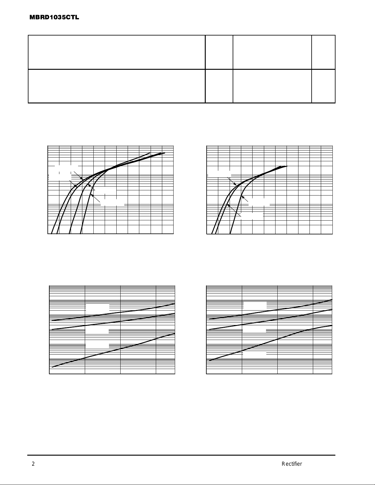
TYPICAL CHARACTERISTICS
V
F
I
R
0.47
0.41
0.56
0.55
2.0
30
0.20
5.0
Volts
mA
100
10
1.0
0.1
, INSTANTANEOUS FORWARD CURRENT (AMPS)
F
I
1E+0
100E–3
10E–3
100
TJ = 125°C
TJ = 100°C
TJ = 25°C
TJ = – 40°C
0.500.30 0.70 0.90
VF, INSTANTANEOUS FORWARD VOLTAGE (VOLTS)
1.100.10
10
1.0
0.1
, INSTANTANEOUS FORWARD CURRENT (AMPS)
F
I
TJ = 125°C
TJ = 25°C
TJ = 100°C
0.500.30 0.70 0.90
VF, MAXIMUM INSTANTANEOUS FORWARD VOLTAGE (VOLTS)
Figure 1. T ypical Forward Voltage Per Leg Figure 2. Maximum Forward Voltage Per Leg
1E+0
100E–3
TJ = 125°C
10E–3
TJ = 125°C
1.100.10
1E–3
100E–6
, REVERSE CURRENT (AMPS)
R
I
10E–6
1E–6
TJ = 100°C
TJ = 25°C
10 20 30
VR, REVERSE VOLTAGE (VOLTS)
Figure 3. T ypical Reverse Current Per Leg
1E–3
100E–6
10E–6
R
I , MAXIMUM REVERSE CURRENT (AMPS)
350
1E–6
Figure 4. Maximum Reverse Current Per Leg
TJ = 100°C
TJ = 25°C
10 20 30
VR, REVERSE VOLTAGE (VOLTS)
2 Rectifier Device Data
350
Page 3

8.0
7.0
6.0
5.0
4.0
3.0
2.0
1.0
, AVERAGE FORW ARD CURRENT (AMPS)
O
I
0
MBRD1035CTL
, AVERAGE POWER DISSIPATION (WA TTS)
FO
P
4.0
3.5
3.0
2.5
2.0
1.5
1.0
0.5
0
Ipk/Io = 10
Ipk/Io = 20
1.00
SQUARE WAVE
(50% DUTY CYCLE)
Ipk/Io =
p
Ipk/Io = 5
3.0 4.0 5.0 6.0 7.0 8.0
2.0
IO, AVERAGE FORW ARD CURRENT (AMPS)
dc
SQUARE WAVE
(50% DUTY CYCLE)
Ipk/Io =
p
Ipk/Io = 5
Ipk/Io = 10
Ipk/Io = 20
freq = 20 kHz
6020 40 80 100 140
TL, LEAD TEMPERATURE (
°
1200
C)
Figure 5. Current Derating Per Leg Figure 6. Forward Power Dissipation Per Leg
dc
1000
C, CAPACITANCE (pF)
100
10
TJ = 25°C
0
510152025
VR, REVERSE VOLTAGE (VOLTS)
Figure 7. Capacitance Per Leg
125
°
115
105
95
85
75
, DERATED OPERATING TEMPERATURE ( C)
J
65
T
Figure 8. T ypical Operating Temperature
R
= 2.43°C/W
q
JA
R
= 48°C/W
q
JA
R
= 67.5°C/W
q
JA
R
= 84°C/W
q
JA
VR, DC REVERSE VOLTAGE (VOLTS)
Derating Per Leg *
* Reverse power dissipation and the possibility of thermal runaway must be considered when operating this device under any reverse voltage conditions. Calculations of TJ therefore must include forward and reverse power effects. The allowable operating
TJ may be calculated from the equation: TJ = T
r(t) = thermal impedance under given conditions,
Pf = forward power dissipation, and
Pr = reverse power dissipation
This graph displays the derated allowable TJ due to reverse bias under DC conditions only and is calculated as TJ = T
where r(t) = Rthja. For other power applications further calculations must be performed.
– r(t)(Pf + Pr) where
Jmax
250
Jmax
R
q
= 25°C/W
JA
30 355101520
– r(t)Pr,
3Rectifier Device Data
Page 4

MBRD1035CTL
D
1.0
50%(DUTY CYCLE)
20%
10%
5.0%
0.1
SINGLE PULSE
2.0%
1.0%
R
= R
• r
tjl(t)
tjl
(t)
0.01
, TRANSIENT THERMAL RESISTANCE (NORMALIZE
(t)
r
0.0001 0.001 0.01
0.10.00001
t, TIME (s)
1.0
10 100 1000
Figure 9. Thermal Response Junction to Case (Per Leg)
1.0E+00
1.0E–01
1.0E–02
1.0E–03
1.0E–04
(t)
r , TRANSIENT THERMAL RESISTANCE (NORMALIZED)
50% (DUTY CYCLE)
20%
10%
5.0%
2.0%
1.0%
SINGLE PULSE
0.0001 0.001 0.01 1.0
R
tjl(t)
0.10.00001
t, TIME (s)
= R
• r
tjl
(t)
10 100 10000
1000
Figure 10. Thermal Response Junction to Ambient (Per Leg)
4 Rectifier Device Data
Page 5

MBRD1035CTL
P ACKAGE DIMENSIONS
NOTES:
SEATING
–T–
PLANE
B
V
S
R
4
A
123
K
F
L
D
2 PL
G
0.13 (0.005) T
C
E
Z
U
J
H
M
1. DIMENSIONING AND TOLERANCING PER ANSI
Y14.5M, 1982.
2. CONTROLLING DIMENSION: INCH.
DIM MIN MAX MIN MAX
A 0.235 0.250 5.97 6.35
B 0.250 0.265 6.35 6.73
C 0.086 0.094 2.19 2.38
D 0.027 0.035 0.69 0.88
E 0.033 0.040 0.84 1.01
F 0.037 0.047 0.94 1.19
G 0.180 BSC 4.58 BSC
H 0.034 0.040 0.87 1.01
J 0.018 0.023 0.46 0.58
K 0.102 0.114 2.60 2.89
L 0.090 BSC 2.29 BSC
R 0.175 0.215 4.45 5.46
S 0.020 0.050 0.51 1.27
U 0.020 ––– 0.51 –––
V 0.030 0.050 0.77 1.27
Z 0.138 ––– 3.51 –––
MILLIMETERSINCHES
CASE 369A–13
ISSUE Y
5Rectifier Device Data
Page 6

MBRD1035CTL
Motorola reserves the right to make changes without further notice to any products herein. Motorola makes no warranty , representation or guarantee regarding
the suitability of its products for any particular purpose, nor does Motorola assume any liability arising out of the application or use of any product or circuit, and
specifically disclaims any and all liability, including without limitation consequential or incidental damages. “T ypical” parameters which may be provided in Motorola
data sheets and/or specifications can and do vary in different applications and actual performance may vary over time. All operating parameters, including “Typicals”
must be validated for each customer application by customer’s technical experts. Motorola does not convey any license under its patent rights nor the rights of
others. Motorola products are not designed, intended, or authorized for use as components in systems intended for surgical implant into the body, or other
applications intended to support or sustain life, or for any other application in which the failure of the Motorola product could create a situation where personal injury
or death may occur. Should Buyer purchase or use Motorola products for any such unintended or unauthorized application, Buyer shall indemnify and hold Motorola
and its officers, employees, subsidiaries, affiliates, and distributors harmless against all claims, costs, damages, and expenses, and reasonable attorney fees
arising out of, directly or indirectly, any claim of personal injury or death associated with such unintended or unauthorized use, even if such claim alleges that
Motorola was negligent regarding the design or manufacture of the part. Motorola and are registered trademarks of Motorola, Inc. Motorola, Inc. is an Equal
Opportunity/Affirmative Action Employer.
How to reach us:
USA/EUROPE /Locations Not Listed: Motorola Literature Distribution; JAPAN: Nippon Motorola Ltd.: SPD, Strategic Planning Office, 141,
P.O. Box 5405, Denver, Colorado 80217. 1–303–675–2140 or 1–800–441–2447 4–32–1 Nishi–Gotanda, Shagawa–ku, Tokyo, Japan. 03–5487–8488
Customer Focus Center: 1–800–521–6274
Mfax: RMFAX0@email.sps.mot.com – TOUCHTONE 1–602–244–6609 ASIA / PACIFIC: Motorola Semiconductors H.K. Ltd.; 8B Tai Ping Industrial Park,
Moto rola Fax Bac k System – US & Canada ONLY 1–800–774–1848 51 Ting Kok Road, Tai Po, N.T., Hong Kong. 852–26629298
HOME PAGE: http://motorola.com/sps/
6 Rectifier Device Data
– http://sps.motorola.com/mfax/
◊
Mfax is a trademark of Motorola, Inc.
MBRD1035CTL/D
 Loading...