

Page 1
SEMICONDUCTOR TECHNICAL DATA
Order this document
by MBRB4030/D
Using the Schottky Barrier principle with a proprietary barrier metal. These
state–of–the–art devices have the following features:
• Guardring for Stress Protection
• Maximum Die Size
• 150°C Operating Junction Temperature
• Short Heat Sink Tab Manufactured – Not Sheared
Mechanical Characteristics
• Case: Epoxy, Molded
• Weight: 1.7 Grams (approximately)
• Finish: All External Surfaces Corrosion Resistant and Terminal
Leads Readily Solderable
• Shipped 50 Units per Plastic Tube
• Available in 24 mm Tape and Reel, 800 Units per 13
Adding a “T4” Suffix to the Part Number
• Marking: B4030
″ Reel by
1
3
4
MAXIMUM RATINGS
Rating Symbol Value Unit
Peak Repetitive Reverse Voltage
Working Peak Reverse Voltage
DC Blocking Voltage
Average Rectified Forward Current
(At Rated VR) TC = +115°C (1)
Peak Repetitive Forward Current
(At Rated VR, Square Wave, 20 kHz) TC = + 112°C
Nonrepetitive Peak Surge Current
(Surge Applied at Rated Load Conditions Halfwave, Single Phase, 60 Hz)
Peak Repetitive Reverse Surge Current (2.0 µs, 1.0 kHz) I
Storage Temperature T
Operating Junction Temperature T
Voltage Rate of Change (Rated VR) dv/dt 10,000 V/µs
Reverse Energy (Unclamped Inductive Surge) (Inductance = 3 mH), Tc = 25°C W 600 mJ
THERMAL CHARACTERISTICS
Thermal Resistance – Junction to Case R
Thermal Resistance – Junction to Ambient (2) R
ELECTRICAL CHARACTERISTICS
Maximum Instantaneous Forward V oltage (1 and 3), per Device
(IF = 20 A, TC = + 25°C)
(IF = 20 A, TC = +150°C)
(IF = 40 A, TC = + 25°C)
(IF = 40 A, TC = +150°C)
Maximum Instantaneous Reverse Current (3), per Device
(Rated DC Voltage, TC = + 25°C)
(Rated DC Voltage, TC = +125°C)
(1) Rating applies when pins 1 and 3 are connected.
(2) Rating applies when surface mounted on the miniumum pad size recommended.
(3) Pulse Test: Pulse Width = 300 µs, Duty Cycle ≤ 2.0%
SWITCHMODE is a trademark of Motorola, Inc.
Preferred devices are Motorola recommended choices for future use and best overall value.
V
RRM
V
RWM
V
I
F(AV)
I
FRM
I
FSM
RRM
θJC
θJA
V
I
R
stg
J
F
R
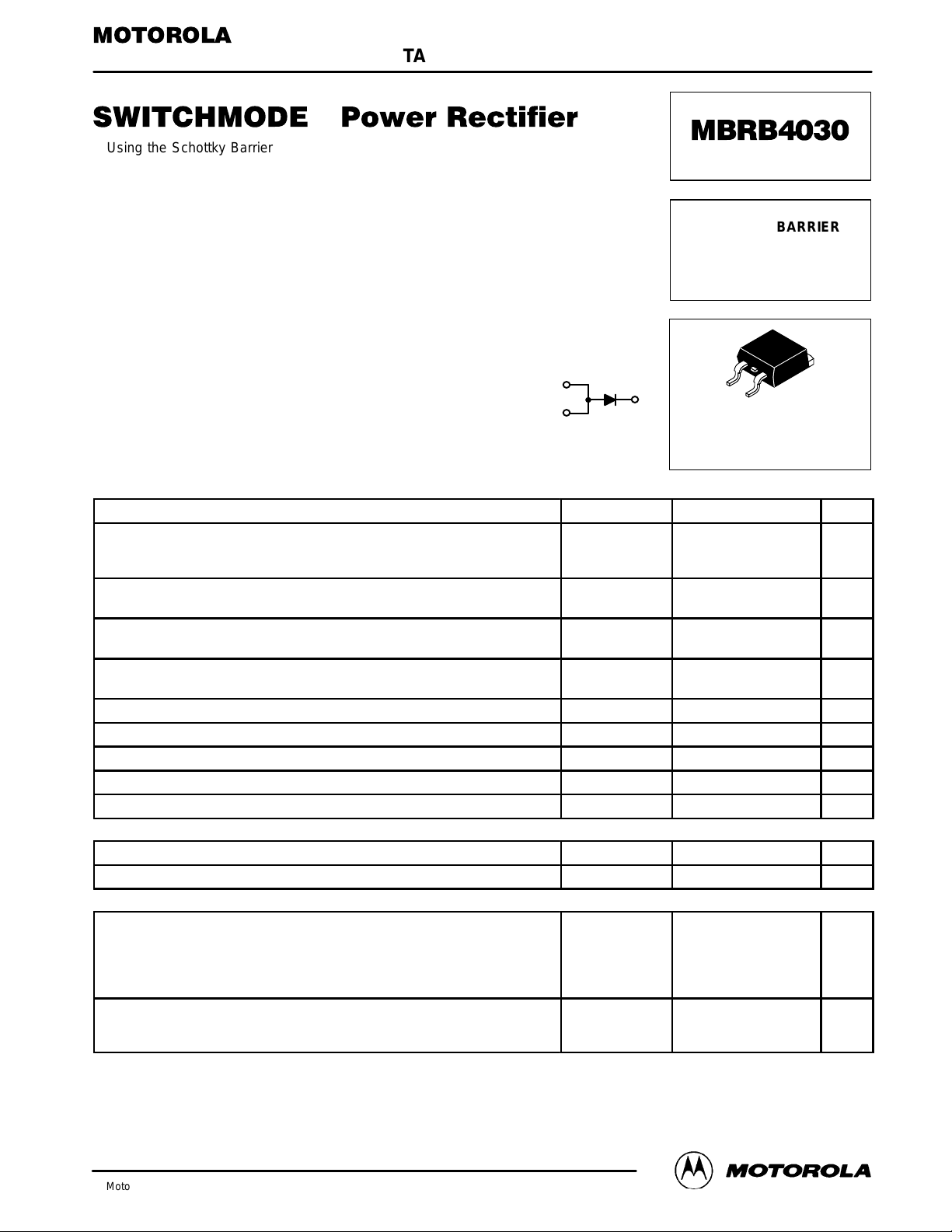
Motorola Preferred Device
SCHOTTKY BARRIER
RECTIFIER
40 AMPERES
30 VOLTS
4
1
3
CASE 418B–02
D2PAK
30
40 A
80 A
300 A
2.0 A
– 65 to +150 °C
– 65 to +150 °C
1.0 °C/W
50 °C/W
0.46
0.34
0.55
0.45
0.35
150
V
V
mA
Rectifier Device Data
Motorola, Inc. 1996
1
Page 2

MBRB4030
7
ELECTRICAL CHARACTERISTICS
100
(PIN 1 SHORTED TO PIN 3)
, INSTANTANEOUS FORWARD CURRENT (mA)
F
I
0.01
10
1.0
0.1
1.0
0.1
TJ = 150°C
100°C
VF, INSTANTANEOUS VOLTAGE (V)
25°C
Figure 1. Maximum Forward V oltage
TJ = 150°C
100°C
100
10
1.0
(PIN 1 SHORTED TO PIN 3)
, INSTANTANEOUS FORWARD CURRENT (mA)
F
I
0.80.60.40.20
0.70.50.30.1 0.50.30.2
0.1
VF, INSTANTANEOUS VOLTAGE (V)
Figure 2. T ypical Forward Voltage
1.0
0.1
0.01
100°C
TJ = 150°C
25°C
TJ = 150°C
100°C
0.60.40.10
0.
, REVERSE CURRENT (A)
R
I
10
10
10
–3
–4
–5
25°C
205 20155
VR, REVERSE VOLTAGE (V)
Figure 3. Maximum Reverse Current
4
10
C, CAPACITANCE (pF)
1000
1
–3
10
, REVERSE CURRENT (A)
R
I
–4
10
–5
10
302515100
TYPICAL
VR, REVERSE VOLTAGE (V)
MAXIMUM
25°C
3025100
VR, REVERSE VOLTAGE (V)
Figure 4. T ypical Reverse Current
TJ = 25°C
10
Figure 5. Maximum and T ypical Capacitance
2
Rectifier Device Data
Page 3

ELECTRICAL CHARACTERISTICS
MBRB4030
, AVERAGE FORW ARD CURRENT (A)
F(AV)
I
, AVERAGE FORW ARD CURRENT (A)
F(AV)
I
70
60
50
40
30
20
(PIN 1 SHORTED TO PIN 3)
10
0
12
10
8
6
4
(PIN 1 SHORTED TO PIN 3)
2
0
20
DC
SQUARE WAVE
π
(RESISTIVE LOAD)
10
20
50
TA, AMBIENT TEMPERATURE (°C)
SURFACE MOUNTED ON
MINIMUM RECOMMENDED
PAD SIZE
I
PK
I
AV
100
SQUARE WAVE
DC
π
(RESISTIVE LOAD)
I
PK
I
AV
10
20
130110 150
TC, CASE TEMPERATURE (°C)
= 5.0
(CAPACITIVE
LOAD)
140120100
, AVERAGE FORW ARD CURRENT (A)
F(AV)
I
15
10
(PIN 1 SHORTED TO PIN 3)
5
0
Figure 6. Current Derating, Infinite Heatsink Figure 7. Current Derating
(PIN 1 SHORTED TO PIN 3)
, AVERAGE FORWARD POWER DISSIPATION (WATTS)
F(AV)
P
50
40
30
20
10
π
(RESISTIVE LOAD)
I
PK
= 5.0
AV
(CAPACITIVE
LOAD)
I
10
20
DC
0
20010
I
, AVERAGE FORW ARD CURRENT (A)
F(AV )
DC
π
(RESISTIVE LOAD)
SQUARE WAVE
10
20
TA, AMBIENT TEMPERATURE (°C)
I
PK
I
AV
R
θ
JA
= 5.0
(CAPACITIVE
LOAD)
= 50°C/W
150100050
Figure 8. Current Derating, Free Air Figure 9. Forward Power Dissipation
R
= 25°C/W
θ
JA
= 5.0
(CAPACITIVE
LOAD)
150
TJ = 150°C
SQUARE WAVE
705030
6040 80
1.0
0.1
RESISTANCE (NORMALIZED)
R(t), EFFECTIVE TRANSIENT THERMAL
0.01
Rectifier Device Data
SINGLE PULSE
t
p
∆
TJL = Ppk • R
where
∆
TJL = the increase in junction temperature above the lead temperature
r(t) = normalized value of transient thermal resistance at time, t, for example,
r(t) = r(t1 + tp) = normalized value of transient thermal resistance at time, t
101.0 1000
t, TIME (ms)
Figure 10. Thermal Response
P
pk
t
1
[D + (1 – D)
θ
JL
P
pk
DUTY CYCLE, D = tp/t
PEAK POWER, Ppk, is peak of an
equivalent square power pulse.
TIME
•
r(t1 + tp) + r(tp) – r(t1)]
1000.1
1
+ tp.
1
3
Page 4

MBRB4030
–T–
SEATING
PLANE
G
B
4
231
S
D
3 PL
0.13 (0.005) T
M
P ACKAGE DIMENSIONS
C
E
V
A
K
J
H
CASE 418B–02
ISSUE B
NOTES:
1. DIMENSIONING AND TOLERANCING PER ANSI
Y14.5M, 1982.
2. CONTROLLING DIMENSION: INCH.
DIM MIN MAX MIN MAX
A 0.340 0.380 8.64 9.65
B 0.380 0.405 9.65 10.29
C 0.160 0.190 4.06 4.83
D 0.020 0.035 0.51 0.89
E 0.045 0.055 1.14 1.40
G 0.100 BSC 2.54 BSC
H 0.080 0.1 10 2.03 2.79
J 0.018 0.025 0.46 0.64
K 0.090 0.1 10 2.29 2.79
S 0.575 0.625 14.60 15.88
V 0.045 0.055 1.14 1.40
STYLE 3:
PIN 1. ANODE
2. CATHODE
3. ANODE
4. CATHODE
MILLIMETERSINCHES
Motorola reserves the right to make changes without further notice to any products herein. Motorola makes no warranty , representation or guarantee regarding
the suitability of its products for any particular purpose, nor does Motorola assume any liability arising out of the application or use of any product or circuit, and
specifically disclaims any and all liability, including without limitation consequential or incidental damages. “T ypical” parameters which may be provided in Motorola
data sheets and/or specifications can and do vary in different applications and actual performance may vary over time. All operating parameters, including “Typicals”
must be validated for each customer application by customer’s technical experts. Motorola does not convey any license under its patent rights nor the rights of
others. Motorola products are not designed, intended, or authorized for use as components in systems intended for surgical implant into the body, or other
applications intended to support or sustain life, or for any other application in which the failure of the Motorola product could create a situation where personal injury
or death may occur. Should Buyer purchase or use Motorola products for any such unintended or unauthorized application, Buyer shall indemnify and hold Motorola
and its officers, employees, subsidiaries, affiliates, and distributors harmless against all claims, costs, damages, and expenses, and reasonable attorney fees
arising out of, directly or indirectly, any claim of personal injury or death associated with such unintended or unauthorized use, even if such claim alleges that
Motorola was negligent regarding the design or manufacture of the part. Motorola and are registered trademarks of Motorola, Inc. Motorola, Inc. is an Equal
Opportunity/Affirmative Action Employer.
How to reach us:
USA/EUROPE/Locations Not Listed: Motorola Literature Distribution; JAPAN: Nippon Motorola Ltd.; Tatsumi–SPD–JLDC, 6F Seibu–Butsuryu–Center,
P.O. Box 5405, Denver, Colorado 80217. 303–675–2140 or 1–800–441–2447 3–14–2 T atsumi Koto–Ku, Tokyo 135, Japan. 81–3–3521–8315
Mfax: RMFAX0@email.sps.mot.com – TOUCHTONE 602–244–6609 ASIA /PACIFIC: Motorola Semiconductors H.K. Ltd.; 8B Tai Ping Industrial Park,
INTERNET: http://Design–NET.com 51 Ting Kok Road, Tai Po, N.T., Hong Kong. 852–26629298
4
CODELINE TO BE PLACED HERE
◊
Mfax is a trademark of Motorola, Inc.
Rectifier Device Data
MBRB4030/D
 Loading...