

Page 1
SEMICONDUCTOR TECHNICAL DATA
Order this document
by MBRB1545CT/D
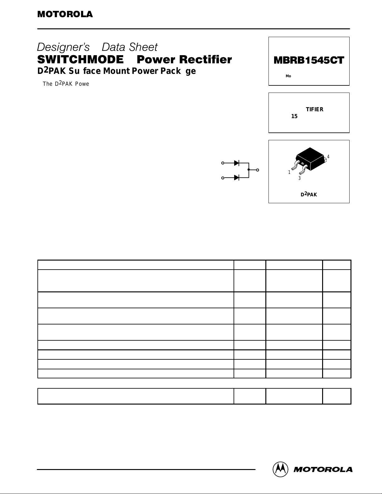
D2PAK Surface Mount Power Package
The D2PAK Power Rectifier employs the Schottky Barrier principle with a
platinum barrier metal. These state-of-the-art devices have the following
features:
• Center-Tap Configuration
• Guardring for Stress Protection
• Low Forward Voltage
• 150°C Operating Junction Temperature
• Epoxy Meets UL94, VO at 1/8″
• Guaranteed Reverse Avalanche
• Short Heat Sink Tab Manufactured — Not Sheared!
• Similar in Size to the Industry Standard TO-220 Package
Mechanical Characteristics
• Case: Epoxy, Molded
• Weight: 1.7 grams (approximately)
• Finish: All External Surfaces Corrosion Resistant and Terminal Leads are
Readily Solderable
• Lead and Mounting Surface Temperature for Soldering Purposes: 260°C
Max. for 10 Seconds
• Shipped 50 units per plastic tube
• Available in 24 mm Tape and Reel, 800 units per 13″ reel by adding a “T4”
suffix to the part number
• Marking: B1545T
1
3
Motorola Preferred Device
SCHOTTKY BARRIER
RECTIFIER
15 AMPERES
45 VOLTS
4
1
3
CASE 418B-02
D2PAK
4
MAXIMUM RATINGS, PER LEG
Rating Symbol Value Unit
Peak Repetitive Reverse Voltage
Working Peak Reverse Voltage
DC Blocking Voltage
Average Rectified Forward Current
(Rated VR) TC = 105°C Total Device
Peak Repetitive Forward Current
(Rated VR, Square Wave, 20 kHz), TC = 105°C
Non-repetitive Peak Surge Current
(Surge applied at rated load conditions halfwave, single phase, 60 Hz)
Peak Repetitive Reverse Surge Current (2.0 µs, 1.0 kHz) I
Storage Temperature T
Operating Junction Temperature T
Voltage Rate of Change (Rated VR) dv/dt 10000 V/µs
V
RRM
V
RWM
V
I
F(AV)
I
FRM
I
FSM
RRM
stg
45 Volts
R
7.5
15
15 Amps
150 Amps
1.0 Amp
–65 to +175 °C
J
–65 to +150 °C
Amps
THERMAL CHARACTERISTICS, PER LEG
Thermal Resistance — Junction to Case
— Junction to Ambient (1)
(1) When mounted using minimum recommended pad size on FR-4 board.
Designer’s Data for “Worst Case” Conditions — The Designer’s Data Sheet permits the design of most circuits entirely from the information presented. SOA Limit
curves —representing boundaries on device characteristics — are given to facilitate “worst case” design.
Designer’s and SWITCHMODE are trademarks of Motorola, Inc.
Thermal Clad is a trademark of the Bergquist Company
Preferred devices are Motorola recommended choices for future use and best overall value.
R
R
θJC
θJA
2.0
50
°C/W
Rev 2
Rectifier Device Data
Motorola, Inc. 1996
1
Page 2
MBRB1545CT
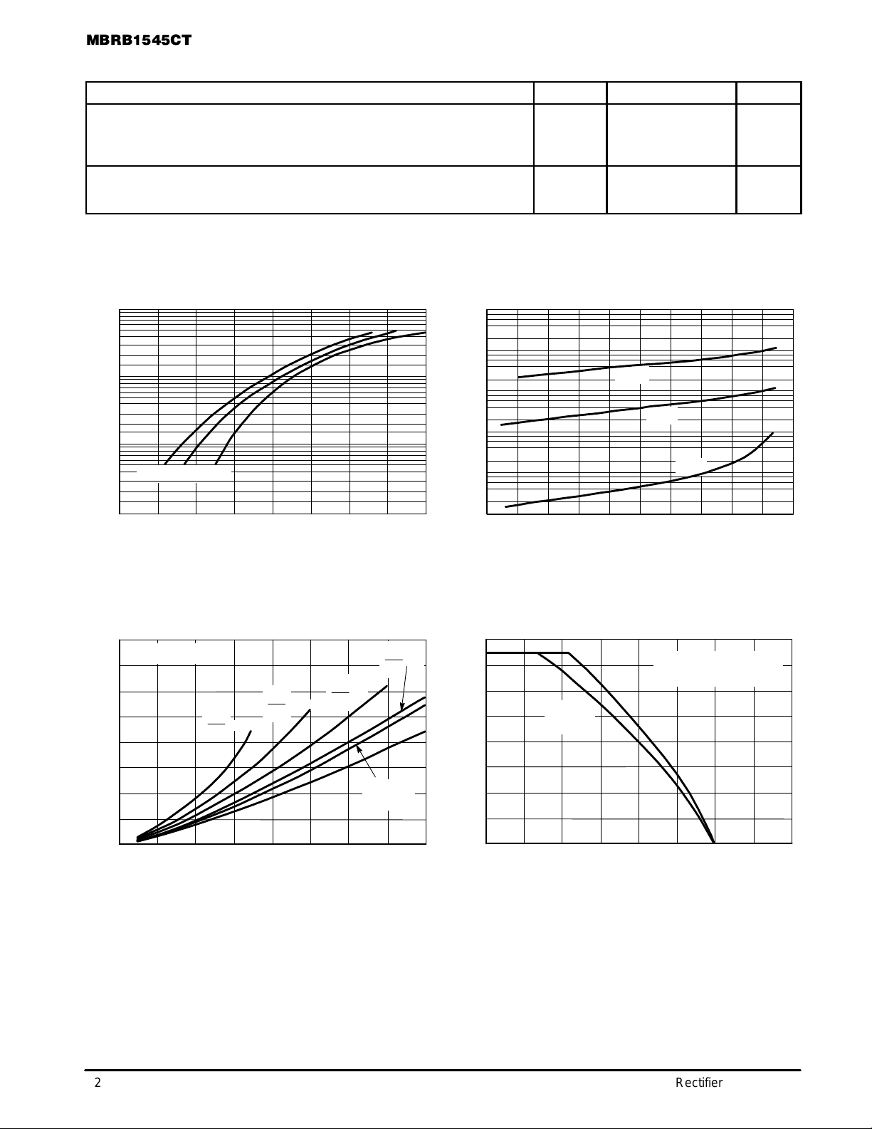
ELECTRICAL CHARACTERISTICS, PER LEG
Rating Symbol Value Unit
Maximum Instantaneous Forward Voltage (2)
(iF = 7.5 Amps, TJ = 125°C)
(iF = 15 Amps, TJ = 125°C)
(iF = 15 Amps, TJ = 25°C)
Maximum Instantaneous Reverse Current (2)
(Rated dc Voltage, TJ = 125°C)
(Rated dc Voltage, TJ = 25°C)
(2) Pulse Test: Pulse Width = 300 µs, Duty Cycle ≤2.0%.
50
30
20
10
3
2
1
0.5
, INSTANTANEOUS FORWARD CURRENT (AMPS)
F
i
Figure 1. T ypical Forward Voltage, Per Leg
25°C85°C125°C
0.50.40.30.20.1
0.6 0.7 0.8 0.9
vF, INSTANTANEOUS FORWARD VOLTAGE (VOLTS)
0.1
0.01
, REVERSE LEAKAGE CURRENT (mA)
R
I
0.001
v
10
F
i
R
1
0
10
20
VR, REVERSE VOLTAGE (VOLTS)
0.57
0.72
0.84
15
0.1
125°C
85°C
Figure 2. T ypical Reverse Current, Per Leg
Volts
mA
25°C
504030
16
14
12
10
, AVERAGE FORWARD POWER DISSIPATION (WATTS)
F(AV)
P
= 5
SQUARE
I
PK
I
AV
WAVE
DC
=
π
1614121086420
TJ = 125°C
I
I
PK
= 10
I
= 20
AV
I
PK
I
8
6
4
2
0
I
AV
, AVERAGE FORW ARD CURRENT (AMPS)
F(AV)
I
PK
AV
16
14
12
10
8
6
4
, AVERAGE FORW ARD CURRENT (AMPS)
2
F(AV)
I
DC
SQUARE
WAVE
TC, CASE TEMPERATURE (
Figure 3. T ypical Forward Power Dissipation Figure 4. Current Derating, Case
RATED VOLTAGE APPLIED
R
°
C/W
= 2
θ
JC
150145140135130125120
155 160
°
C)
2
Rectifier Device Data
Page 3

INFORMATION FOR USING THE D2PAK SURFACE MOUNT PACKAGE
MINIMUM RECOMMENDED FOOTPRINTS FOR SURFACE MOUNTED APPLICATIONS
Surface mount board layout is a critical portion of the total
design. The footprint for the semiconductor packages must be
the correct size to insure proper solder connection interface
0.450
11.43
MBRB1545CT
between the board and the package. With the correct pad
geometry, the packages will self align when subjected to a
solder reflow process.
0.70
17.78
0.0625
1.587
0.08
2.032
0.350
8.89
D2P AK POWER DISSIPATION
The power dissipation of the D2P AK is a function of the drain
pad size. This can vary from the minimum pad size for
soldering to a pad size given for maximum power dissipation.
Power dissipation for a surface mount device is determined by
T
R
, the maximum rated junction temperature of the die,
J(max)
, the thermal resistance from the device junction to
θJA
ambient; and the operating temperature, TA. Using the values
provided on the data sheet for the D2P AK package, PD can be
calculated as follows:
PD =
T
J(max)
R
θJA
– T
A
The values for the equation are found in the maximum
ratings table on the data sheet. Substituting these values into
GENERAL SOLDERING PRECAUTIONS
The melting temperature of solder is higher than the rated
temperature of the device. When the entire device is heated
to a high temperature, failure to complete soldering within a
short time could result in device failure. Therefore, the
following items should always be observed in order to
minimize the thermal stress to which the devices are
subjected.
• Always preheat the device.
• The delta temperature between the preheat and soldering
should be 100°C or less.*
• When preheating and soldering, the temperature of the
leads and the case must not exceed the maximum
temperature ratings as shown on the data sheet. When
using infrared heating with the reflow soldering method,
the difference shall be a maximum of 10°C.
• The soldering temperature and time shall not exceed
260°C for more than 5 seconds.
0.15
3.81
inches
mm
the equation for an ambient temperature TA of 25°C, one can
calculate the power dissipation of the device which in this case
is 2.5 watts.
150°C – 25°C
PD =
50°C/W
= 2.5 watts
The 50°C/W for the D2PAK package assumes the
recommended drain pad area of 158K mil2 on FR-4 glass
epoxy printed circuit board to achieve a power dissipation of
2.5 watts using the footprint shown. Another alternative is to
use a ceramic substrate or an aluminum core board such as
Thermal Clad. By using an aluminum core board material
such as Thermal Clad, the power dissipation can be doubled
using the same footprint.
• When shifting from preheating to soldering, the maximum
temperature gradient shall be 5°C or less.
• After soldering has been completed, the device should be
allowed to cool naturally for at least three minutes.
Gradual cooling should be used as the use of forced
cooling will increase the temperature gradient and result
in latent failure due to mechanical stress.
• Mechanical stress or shock should not be applied during
cooling
* Soldering a device without preheating can cause excessive
thermal shock and stress which can result in damage to the
device.
* Due to shadowing and the inability to set the wave height to
incorporate other surface mount components, the D2PAK is
not recommended for wave soldering.
Rectifier Device Data
3
Page 4

MBRB1545CT
RECOMMENDED PROFILE FOR REFLOW SOLDERING
For any given circuit board, there will be a group of control
settings that will give the desired heat pattern. The operator
must set temperatures for several heating zones, and a figure
for belt speed. T aken together , these control settings make up
a heating “profile” for that particular circuit board. On
machines controlled by a computer, the computer remembers
these profiles from one operating session to the next. Figure
5 shows a typical heating profile for use when soldering the
D2P AK to a printed circuit board. This profile will vary among
soldering systems but it is a good starting point. Factors that
can affect the profile include the type of soldering system in
use, density and types of components on the board, type of
solder used, and the type of board or substrate material being
used. This profile shows temperature versus time. The line on
the graph shows the actual temperature that might be
experienced on the surface of a test board at or near a central
solder joint. The two profiles are based on a high density and
a low density board. The Vitronics SMD310 convection/infrared reflow soldering system was used to generate this
profile. The type of solder used was 62/36/2 Tin Lead Silver
with a melting point between 177–189°C. When this type of
furnace is used for solder reflow work, the circuit boards and
solder joints tend to heat first. The components on the board
are then heated by conduction. The circuit board, because it
has a large surface area, absorbs the thermal energy more
efficiently, then distributes this energy to the components.
Because of this effect, the main body of a component may be
up to 30 degrees cooler than the adjacent solder joints.
200
°
150°C
100
°
°
50
C
C
C
STEP 1
PREHEA T
ZONE 1
“RAMP”
TIME (3 TO 7 MINUTES TOTAL)
STEP 2
VENT
“SOAK”
DESIRED CURVE FOR HIGH
MASS ASSEMBLIES
150°C
100
STEP 3
HEATING
ZONES 2 & 5
“RAMP”
°
C
DESIRED CURVE FOR LOW
STEP 4
HEATING
ZONES 3 & 6
“SOAK”
160°C
140
°
C
MASS ASSEMBLIES
STEP 5
HEATING
ZONES 4 & 7
“SPIKE”
°
C
170
SOLDER IS LIQUID FOR
40 TO 80 SECONDS
(DEPENDING ON
MASS OF ASSEMBLY)
T
MAX
STEP 6
VENT
205
SOLDER JOINT
STEP 7
COOLING
°
TO 219°C
PEAK AT
Figure 5. Typical Solder Heating Profile for D2PAK
4
Rectifier Device Data
Page 5

P ACKAGE DIMENSIONS
MBRB1545CT
–T–
SEATING
PLANE
G
B
4
231
S
D
3 PL
0.13 (0.005) T
M
C
E
A
K
J
H
CASE 418B–02
ISSUE B
NOTES:
V
1. DIMENSIONING AND TOLERANCING PER ANSI
Y14.5M, 1982.
2. CONTROLLING DIMENSION: INCH.
DIM MIN MAX MIN MAX
A 0.340 0.380 8.64 9.65
B 0.380 0.405 9.65 10.29
C 0.160 0.190 4.06 4.83
D 0.020 0.035 0.51 0.89
E 0.045 0.055 1.14 1.40
G 0.100 BSC 2.54 BSC
H 0.080 0.1 10 2.03 2.79
J 0.018 0.025 0.46 0.64
K 0.090 0.1 10 2.29 2.79
S 0.575 0.625 14.60 15.88
V 0.045 0.055 1.14 1.40
STYLE 3:
PIN 1. ANODE
2. CATHODE
3. ANODE
4. CATHODE
MILLIMETERSINCHES
Rectifier Device Data
5
Page 6

MBRB1545CT
Motorola reserves the right to make changes without further notice to any products herein. Motorola makes no warranty , representation or guarantee regarding
the suitability of its products for any particular purpose, nor does Motorola assume any liability arising out of the application or use of any product or circuit, and
specifically disclaims any and all liability, including without limitation consequential or incidental damages. “T ypical” parameters which may be provided in Motorola
data sheets and/or specifications can and do vary in different applications and actual performance may vary over time. All operating parameters, including “Typicals”
must be validated for each customer application by customer’s technical experts. Motorola does not convey any license under its patent rights nor the rights of
others. Motorola products are not designed, intended, or authorized for use as components in systems intended for surgical implant into the body, or other
applications intended to support or sustain life, or for any other application in which the failure of the Motorola product could create a situation where personal injury
or death may occur. Should Buyer purchase or use Motorola products for any such unintended or unauthorized application, Buyer shall indemnify and hold Motorola
and its officers, employees, subsidiaries, affiliates, and distributors harmless against all claims, costs, damages, and expenses, and reasonable attorney fees
arising out of, directly or indirectly, any claim of personal injury or death associated with such unintended or unauthorized use, even if such claim alleges that
Motorola was negligent regarding the design or manufacture of the part. Motorola and are registered trademarks of Motorola, Inc. Motorola, Inc. is an Equal
Opportunity/Affirmative Action Employer.
How to reach us:
USA/EUROPE/Locations Not Listed: Motorola Literature Distribution; JAPAN: Nippon Motorola Ltd.; Tatsumi–SPD–JLDC, 6F Seibu–Butsuryu–Center,
P.O. Box 5405, Denver, Colorado 80217. 303–675–2140 or 1–800–441–2447 3–14–2 Tatsumi Koto–Ku, Tokyo 135, Japan. 81–3–3521–8315
Mfax: RMFAX0@email.sps.mot.com – TOUCHTONE 602–244–6609 ASIA/PACIFIC: Motorola Semiconductors H.K. Ltd.; 8B Tai Ping Industrial Park,
INTERNET: http://Design–NET.com 51 Ting Kok Road, Tai Po, N.T., Hong Kong. 852–26629298
6
CODELINE TO BE PLACED HERE
◊
Mfax is a trademark of Motorola, Inc.
Rectifier Device Data
MBRB1545CT/D
 Loading...