

Page 1
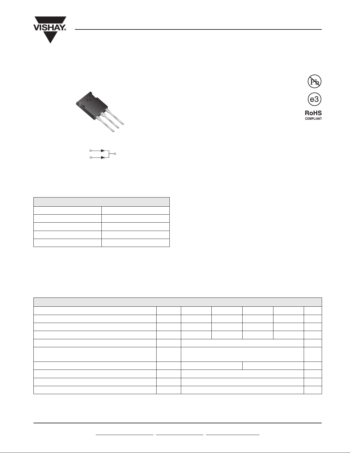
Dual Common-Cathode Schottky Rectifier
3
2
1
TO-247AD (TO-3P)
PIN 1
PIN 3
PRIMARY CHARACTERISTICS
I
F(AV)
V
RRM
I
FSM
V
F
T
max. 150 °C
J
PIN 2
CASE
35 V to 60 V
0.60 V, 0.62 V
40 A
400 A
MBR4035PT thru MBR4060PT
Vishay General Semiconductor
FEATURES
• Guardring for overvoltage protection
• Lower power losses, high efficiency
• Low forward voltage drop
• High forward surge capability
• High frequency operation
• Solder dip 260 °C, 40 s
• Component in accordance to RoHS 2002/95/EC
and WEEE 2002/96/EC
TYPICAL APPLICATIONS
For use in low voltage, high frequency rectifier of
switching mode power supplies, freewheeling diodes,
dc-to-dc converters or polarity protection application.
MECHANICAL DATA
Case: TO-247AD (TO-3P)
Epoxy meets UL 94V-0 flammability rating
Terminals: Matte tin plated leads, solderable per
J-STD-002 and JESD22-B102
E3 suffix for consumer grade, meets JESD 201 class
1A whisker test
Polarity: As marked
Mounting Torque: 10 in-lbs maximum
MAXIMUM RATINGS (TA = 25 °C unless otherwise noted)
PARAMETER SYMBOL MBR4035PT MBR4045PT MBR4050PT MBR4060PT UNIT
Maximum repetitive peak reverse voltage V
Maximum working peak reverse voltage V
Maximum DC blocking voltage V
Maximum average forward rectified current at T
Peak forward surge current, 8.3 ms single
half sine-wave superimposed on rated load per diode
Peak repetitive reverse surge current per diode
Voltage rate of change at (rated V
Operating junction temperature range T
Storage temperature range T
Note:
(1) 2.0 µs pulse width, f = 1.0 kHz
Document Number: 88679
Revision: 25-Mar-08
) dV/dt 10 000 V/µs
R
For technical questions within your region, please contact one of the following:
PDD-Americas@vishay.com
= 125 °C I
C
(1)
, PDD-Asia@vishay.com, PDD-Europe@vishay.com
35 45 50 60 V
RRM
35 45 50 60 V
RWM
35 45 50 60 V
DC
F(AV)
I
400 A
FSM
I
RRM
- 65 to + 150 °C
J
- 65 to + 175 °C
STG
2.0 1.0 A
40 A
www.vishay.com
1
Page 2
MBR4035PT thru MBR4060PT
Vishay General Semiconductor
ELECTRICAL CHARACTERISTICS (TA = 25 °C unless otherwise noted)
PARAMETER TEST CONDITIONS SYMBOL MBR4035PT MBR4045PT MBR4050PT MBR4060PT UNIT
Maximum instantaneous
forward voltage per diode
Maximum instantaneous
reverse current at rated DC
blocking voltage per diode
(1)
(1)
IF = 20 A,
I
= 20 A,
F
I
= 40 A,
F
I
= 40 A,
F
T
= 25 °C
C
T
= 125 °C
C
T
= 25 °C
C
T
= 125 °C
C
TC = 25 °C
T
= 125 °C
C
V
F
I
R
0.70
0.60
0.80
0.75
1.0
100
Note:
(1) Pulse test: 300 µs pulse width, 1 % duty cycle
THERMAL CHARACTERISTICS (TA = 25 °C unless otherwise noted)
PARAMETER SYMBOL MBR4035PT MBR4045PT MBR4050PT MBR4060PT UNIT
Maximum thermal resistance from junction to case per diode R
1.2 °C/W
θJC
0.72
0.62
-
-
mA
V
ORDERING INFORMATION (Example)
PACKAGE PREFERRED P/N UNIT WEIGHT (g) PACKAGE CODE BASE QUANTITY DELIVERY MODE
TO-247AD MBR4045PT-E3/45 6.13 45 30/tube Tube
RATINGS AND CHARACTERISTICS CURVES
(T
= 25 °C unless otherwise noted)
A
50
Resistive or Inductive Load
40
30
20
10
Average Forward Current (A)
0
0
50
Case Temperature (°C)
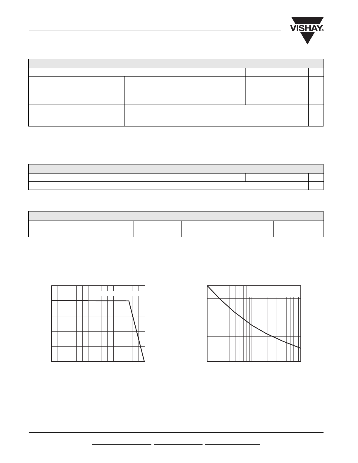
Figure 1. Forward Current Derating Curve
100
150
400
300
200
Peak Fo rward Surge Current (A)
100
1
Number of Cycles at 60 Hz
TJ = TJ Max.
8.3 ms Single Half Sine-Wave
10
100
Figure 2. Maximum Non-Repetitive Peak Forward Surge
Current Per Diode
www.vishay.com For technical questions within your region, please contact one of the following:
2
PDD-Americas@vishay.com
, PDD-Asia@vishay.com, PDD-Europe@vishay.com
Document Number: 88679
Revision: 25-Mar-08
Page 3

MBR4035PT thru MBR4060PT
Vishay General Semiconductor
100
10
1
TJ = 150 °C
Pulse Width = 300 µs
1 % Duty Cycle
TJ = 25 °C
0.1
Instantaneous Forward Current (A)
0.01
0.2
0
MBR4035PT - MBR4045PT
MBR4050PT & MBR4060PT
0.4
0.6
0.8
1.0
1.2
Instantaneous Forward Voltage (V)
Figure 3. Typical Instantaneous Forward Characteristics Per Diode
100
10
1
0.1
0.01
MBR4035PT - MBR4045PT
MBR4050PT & MBR4060PT
TJ = 75 °C
TJ = 25 °C
TJ = 125 °C
10 000
TJ = 25 °C
f = 1.0 MHz
= 50 mVp-p
V
sig
1000
Junction Capacitance (pF)
MBR4035PT - MBR4045PT
100
0.1
MBR4050PT & MBR4060PT
1
10
Reverse Voltage (V)
Figure 5. Typical Junction Capacitance Per Diode
100
10
1
100
Instantaneous Reverse Current (mA)
0.001
0
20
40
60
80
100
Percent of Rated Peak Reverse Voltage (%)
Figure 4. Typical Reverse Characteristics Per Diode
PACKAGE OUTLINE DIMENSIONS in inches (millimeters)
TO-247AD (TO-3P)
0.645 (16.4)
0.625 (15.9)
1
2
3
PIN 1
PIN 3
0.323 (8.2)
0.313 (7.9)
0.170
(4.3)
0.142 (3.6)
0.138 (3.5)
0.086(2.18)
0.076 (1.93)
0.127 (3.22)
0.117 (2.97)
0.048 (1.22)
0.044 (1.12)
PIN 2
CASE
, PDD-Asia@vishay.com, PDD-Europe@vishay.com
Document Number: 88679
Revision: 25-Mar-08
0.245 (6.2)
0.225 (5.7)
0.840 (21.3)
0.820 (20.8)
0.160 (4.1)
0.140 (3.5)
0.795 (20.2)
0.775 (19.6)
0.225 (5.7)
0.205 (5.2)
For technical questions within your region, please contact one of the following:
PDD-Americas@vishay.com
Transient Thermal Impedance (°C/W)
0.1
0.01
0.1
1
10
100
t - Pulse Duration (s)
Figure 6. Typical Transient Thermal Impedance Per Diode
0.203 (5.16)
0.193 (4.90)
30°
10° TYP.
Both Sides
0.118 (3.0)
0.108 (2.7)
0.030 (0.76)
0.020 (0.51)
0.078 (1.98) REF.
10
1° REF.
Both Sides
www.vishay.com
3
Page 4

Legal Disclaimer Notice
Vishay
Disclaimer
ALL PRODUCT, PRODUCT SPECIFICATIONS AND DATA ARE SUBJECT TO CHANGE WITHOUT NOTICE TO IMPROVE
RELIABILITY, FUNCTION OR DESIGN OR OTHERWISE.
Vishay Intertechnology, Inc., its affiliates, agents, and employees, and all persons acting on its or their behalf (collectively,
“Vishay”), disclaim any and all liability for any errors, inaccuracies or incompleteness contained in any datasheet or in any other
disclosure relating to any product.
Vishay makes no warranty, representation or guarantee regarding the suitability of the products for any particular purpose or
the continuing production of any product. To the maximum extent permitted by applicable law, Vishay disclaims (i) any and all
liability arising out of the application or use of any product, (ii) any and all liability, including without limitation special,
consequential or incidental damages, and (iii) any and all implied warranties, including warranties of fitness for particular
purpose, non-infringement and merchantability.
Statements regarding the suitability of products for certain types of applications are based on Vishay’s knowledge of typical
requirements that are often placed on Vishay products in generic applications. Such statements are not binding statements
about the suitability of products for a particular application. It is the customer’s responsibility to validate that a particular
product with the properties described in the product specification is suitable for use in a particular application. Parameters
provided in datasheets and/or specifications may vary in different applications and performance may vary over time. All
operating parameters, including typical parameters, must be validated for each customer application by the customer’s
technical experts. Product specifications do not expand or otherwise modify Vishay’s terms and conditions of purchase,
including but not limited to the warranty expressed therein.
Except as expressly indicated in writing, Vishay products are not designed for use in medical, life-saving, or life-sustaining
applications or for any other application in which the failure of the Vishay product could result in personal injury or death.
Customers using or selling Vishay products not expressly indicated for use in such applications do so at their own risk and agree
to fully indemnify and hold Vishay and its distributors harmless from and against any and all claims, liabilities, expenses and
damages arising or resulting in connection with such use or sale, including attorneys fees, even if such claim alleges that Vishay
or its distributor was negligent regarding the design or manufacture of the part. Please contact authorized Vishay personnel to
obtain written terms and conditions regarding products designed for such applications.
No license, express or implied, by estoppel or otherwise, to any intellectual property rights is granted by this document or by
any conduct of Vishay. Product names and markings noted herein may be trademarks of their respective owners.
Document Number: 91000 www.vishay.com
Revision: 11-Mar-11 1
 Loading...