

Page 1
-
1 -
Macroblock
16-bit Constant Current LED Sink Driver MBI5016
January 2003,V1.2
Features
· 16 constant current output channels
MBI5016CNS
· Adjustable output current through an external resistor
· Serial data in/parallel data out
· Output current: 5-90 mA
· 20MHz clock frequency
MBI5016CF
Product Description
The MBI5016, utilizing the most advanced silicon
technology, is targeted for LED panel display. The
MBI5016 contains CMOS shift registers and latch
functions, converting serial input data into parallel output
format. At output stage, sixteen regulated current sources,
implemented in Bipolar Junction Transistor, were
designed to provide 5-90 mA constant current for driving
the LEDs.
The MBI5016 provides users great flexibility and device performance while using the
MBI5016 in their LED panel system design. Users may adjust the output current of the MBI5016
through an external resistor R-EXT, which gives users flexibility in controlling the light intensity
of LEDs. The MBI5016 guarantees 17V output driving capability, allowing users to connect more
LEDs in series. The high clock frequency, 20 MHz, also satisfies the system requirement of high
volume data transmission.
MBI5016CP
ÓMacroblock, Inc. 2003
Floor 6-4, No. 18, Pu-Ting Rd., Hsinchu, Taiwan 30077, ROC.
TEL: +886-3-579-0068, FAX: +886-3-579-7534 E-mail: info@mblock.com.tw
All specifications are subject to change without notice.
Page 2
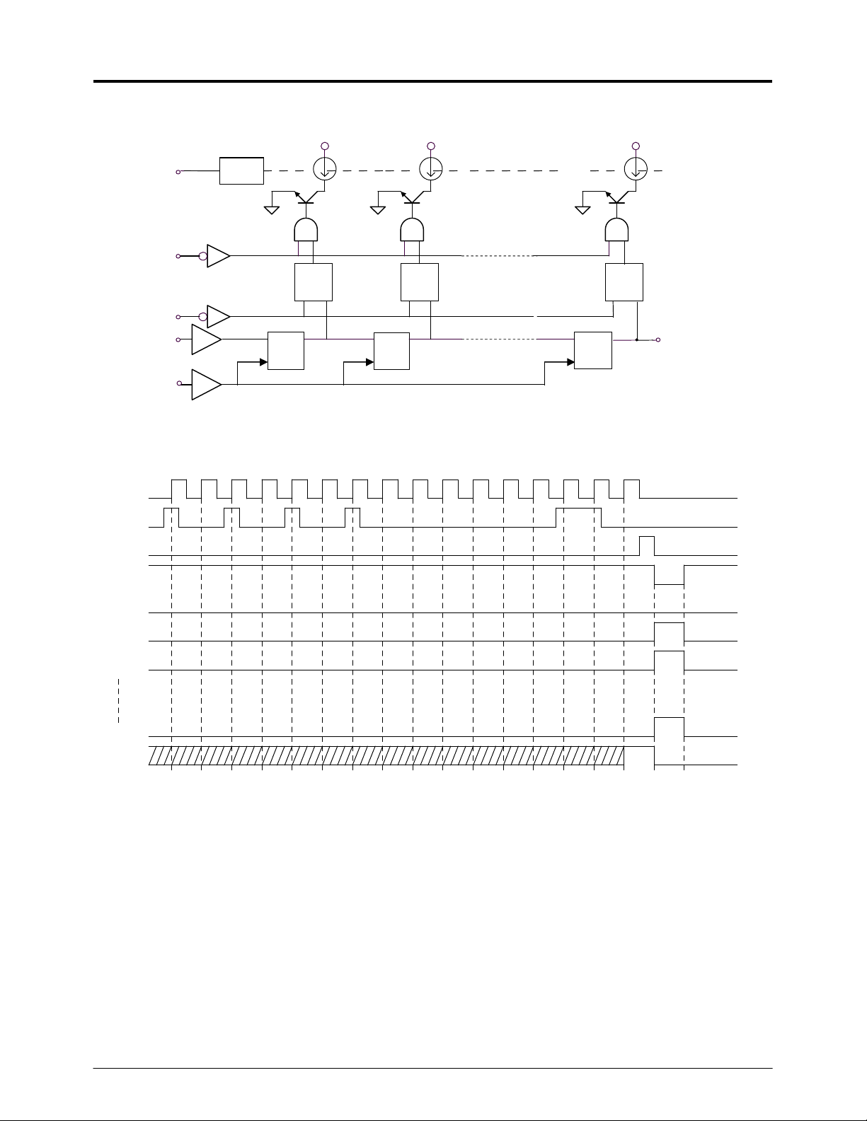
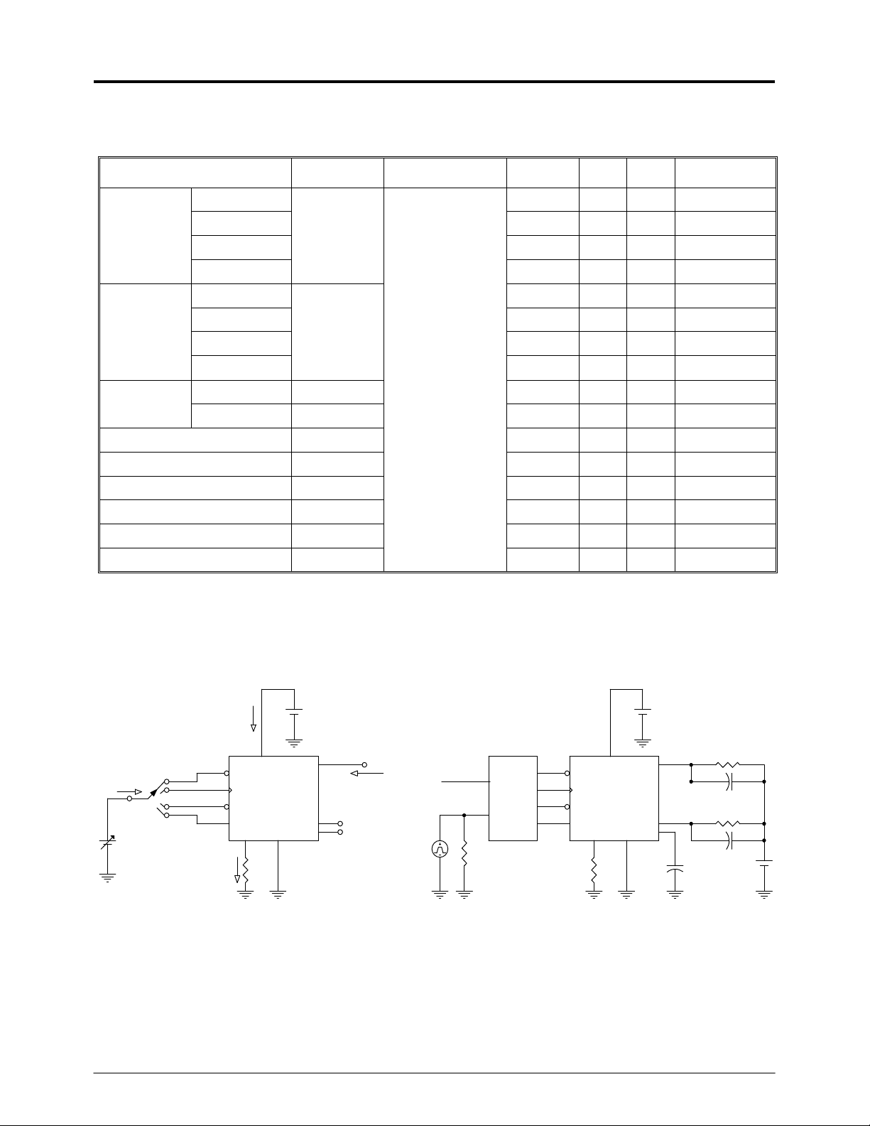
ST ST ST D D D
D CK Q D CK Q D CK Q Q Q Q
MBI5016-V1.2 16-bit Constant Current LED Sink Driver
Block Diagram
R-EXT
I-Ref
/OE
/LE
SDI
CLK
Timing Diagram
CLK
SDI
/LE
/OE
OUT0
OUT1
OUT2
OUT0
OUT1
OUT15
SDO
5V
0V
5V
0V
5V
0V
5V
0V
On
Off
On
Off
On
Off
On
OUT15
SDO
- 2 -
Off
5V
0V
Page 3
MBI5016-V1.2 16-bit Constant Current LED Sink Driver
Terminal Description and Pin Out
Pin No. Pin Name
Function
1 GND GND terminal for control logic.
2 SDI
3 CLK
Input terminal of a serial-data for shift
register
Input terminal of a clock for data shift to
up-edge.
Input terminal of a data strobe. Latches
4 /LE
passes data with "H" level input of
/LE-terminal, and hold data with "L" level
input.
5~20 OUT0~15 Output terminals
Input terminal of output enable. All outputs
21 /OE
(OUT~15) do off with "H" level input of
/OE-terminal, and do on with "L" level
input.
22 SDO
23 R-EXT
Output terminal of a serial-data for next
SDI terminal.
Input terminal of connects with a resister
for setting up all output current.
24 VDD 5V Supply voltage terminal
Truth Table
GND
SDI
CLK
/LE
OUT0
OUT1
OUT2
OUT3
OUT4
OUT5
OUT6
OUT7
24
2
23
3
22
4
21
5
20
6
19
7
18
8
17
9
10
11
1213
16
15
14
VDD1
R-EXT
SDO
/OE
OUT15
OUT14
OUT13
OUT12
OUT11
OUT10
OUT9
OUT8
CLK /LE /OE SDI OUT0…OUT7…OUT15
UP H L D
UP L L D
UP H L D
DOWN
DOWN
X L D
X H D
D
n
No Change D
n+1
D
n+2
D
n+3
Off D
n+3
D
n
n+2 Dn-5
n+2 Dn-5 Dn-13
n-7 Dn-15
D
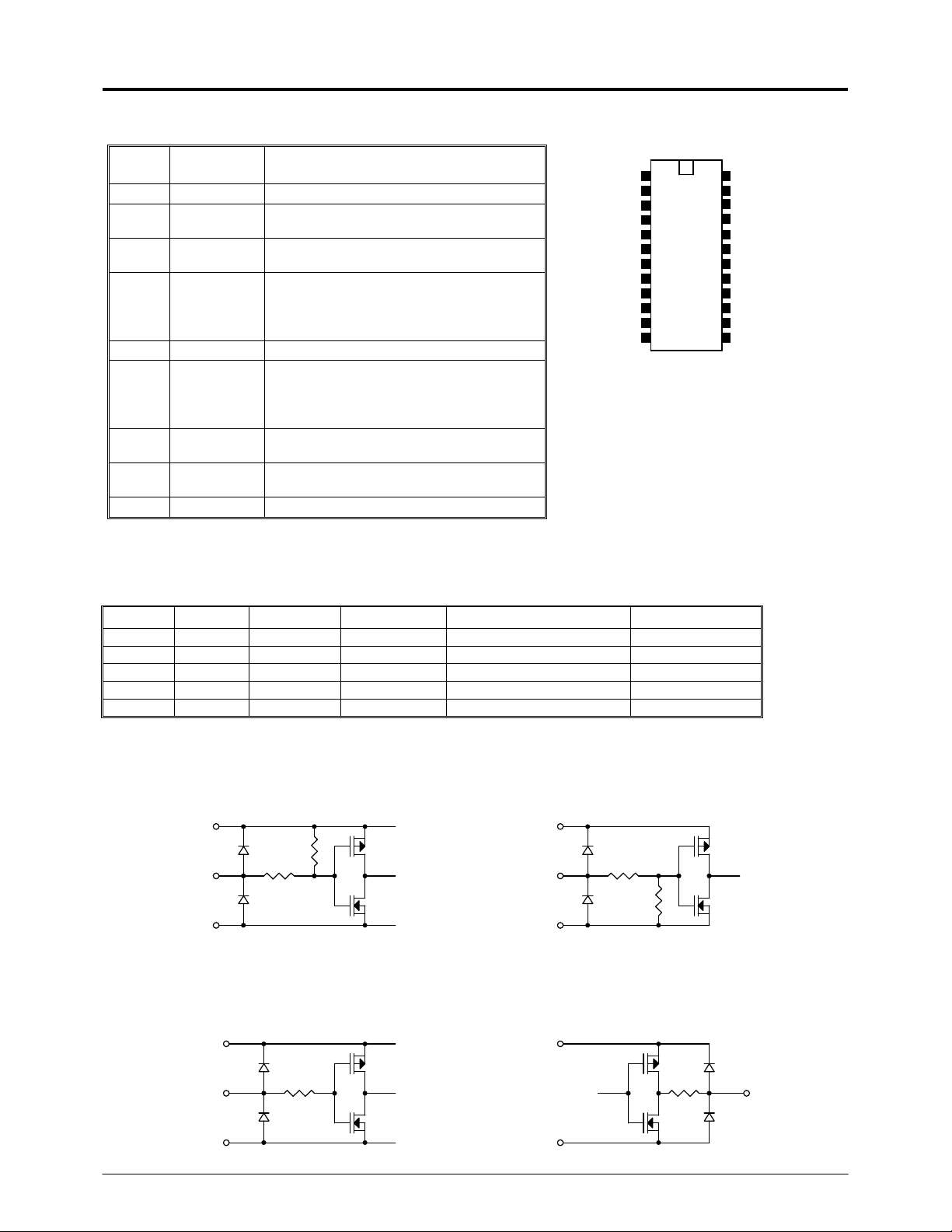
Equivalent Circuits of Inputs and Outputs
1. /OE terminal2. /LE terminal
VDD
/OE
GND
3. CLK, SDI terminal4. SDO terminal
VDD
VDD
/LE
GND
VDD
SDO
D
D
n-13
D
n-15
n-14
n-13
n-13
n-13
CLK, SDI SDO
GND
- 3 -
15th LATCH
DATA
GND
Page 4
MBI5016-V1.2 16-bit Constant Current LED Sink Driver
Maximum Ratings
Characteristic Symbol Rating Unit
Supply Voltage V
Input Voltage V
Output Current I
Output Voltage V
Clock Frequency F
GND Terminal Current I
0~7.0 V
DD
-0.4~VDD + 0.4 V
IN
+90 mA
OUT
-0.5~+17.0 V
OUT
20 MHz
CLK
1440 mA
GND
Power Dissipation 1.78 (CNS type: On PCB, Ta=25°C)
PD
1.00 (CF/CP type: On PCB, Ta=25°C)
Thermal Resistance 82 (CNS type: On PCB)
96, 112 (CF/CP type: On PCB)
Rth(j-a)
°C/W
Operating Temperature Topr -40~+85 °C
Storage Temperature Tstg -55~+150 °C
Recommended Operating Condition
Characteristic Symbol Condition Min. Typ. Max. Unit
W
Supply Voltage V
Output Voltage V
Output Current
- 4.5 5.0 5.5 V
DD
- - - 17.0 V
OUT
I
DC Test Circuit 5 - 90 mA
OUT
IOH SERIAL-OUT - - -1.0 mA
IOL SERIAL-OUT - - 1.0 mA
VIH - 0.7VDD - VDD+0.3
Input Voltage
VIL - -0.3 - 0.3VDD
/LE Pulse Width tw LAT 25 - - ns
CLK Pulse Width tw CLK 25 - - ns
/OE Pulse Width tw EN 400 - - ns
Setup Time for DATA tsetup(D) 20 - - ns
VDD=4.5~5.5V
Hold Time for DATA thold(D) 15 - - ns
Setup Time for LATCH tsetup(L) 20 - - ns
Hold Time for ENABLE thold(L)
Clock Frequency F
Cascade Operation - - 20.0 MHz
CLK
60 - - ns
Ta=85°C (CNS type) - - 0.92
Power Dissipation P
D
Ta=85°C (CF/CP type) - - 0.50
V
W
- 4 -
Page 5

MBI5016-V1.2 16-bit Constant Current LED Sink Driver
Electrical Characteristics
Characteristic Symbol
Input
Voltage
“H” level V
“L” level V
Output Leakage Current
Output
Voltage
SDO
Output Current 1
Current Skew
Output Current 2
Current Skew
Ta = -40~85ºC 0.7V
IH
Ta = -40~85ºC GND - 0.3V
IL
IOH V
VOL I
VOH I
I
VCE=0.8V
OL1
dI
OL1
I
OL2
dI
OL2
IOL=40mA
VCE=0.8V
VCE=1.2V
IOL=80mA
VCE=1.2V
Condition Min. Typ. Max.
DD
=17.0V - - 10 μA
OH
=+1.0mA - - 0.4 V
OL
=-1.0mA 4.6 - - V
OH
R-EXT=865 Ω
(Include Skew)
- 40.0 - mA
- VDD V
DD
R-EXT=865 Ω - ±1.5 ±6.0 %
R-EXT=330 Ω
(Include Skew)
- 80.0 - mA
R-EXT=330 Ω - ±1.5 ±6.0 %
Unit
Pull-up Resistor RIN(up) /OE 150 300 600 KΩ
Pull-down Resistor RIN(down)
I
(off) 1
DD
“OFF”
Supply
Current
IDD(off) 2
IDD(off) 3
IDD(on) 1
R-EXT=OPEN OUT0~15=Off - 8.5 12
R-EXT=865 Ω OUT0~15=Off - 10 12
R-EXT=330 Ω OUT0~15=Off - 11.5 15
R-EXT=865 Ω OUT0~15=On 10 16 22
/LE 85 200 400 KΩ
mA
“ON”
IDD(on) 2
R-EXT=330 Ω OUT0~15=On 18 24.3 38.5
- 5 -
Page 6
MBI5016-V1.2 16-bit Constant Current LED Sink Driver
Switching Characteristics
Characteristic Symbol Condition Min. Typ. Max.
CLK - OUTn - 200 300 ns
Propagation
Delay Time
(“L” to “H”)
/LE - OUTn - 200 300 ns
tpLH
/OE - OUTn - 200 300 ns
CLK - SDO
20 50 70 ns
Inn - OUTn - 200 300 ns
Propagation
Delay Time
(“H” to “L”)
Pulse Width
Set-up Time for LATCH tsetup LAT 10 - 20 ns
/LE - OUTn - 200 300 ns
/OE - OUTn - 200 300 ns
tpHL
VDD=5.0V
VCE=0.8V
VIH=VDD
CLK - SDO
CLK tw CLK-CLK
/LE tw LAT-LAT
VIL=GND
R-EXT=865 Ω
VL=3.4V
RL=65 Ω
20 50 70 ns
15 - 20 ns
20 - 30 ns
CL=10.5pF
Hold Time for LATCH thold LAT 10 - 25 ns
Maximum CLK Rise Time tr - - 5 us
Maximum CLK Fall Time tf - - 5 us
Output Rise Time tor - 150 200 ns
Output Fall Time tof
- 150 200 ns
Unit
Test Circuit for DC Characteristic Test Circuit for AC Characteristic
I
DD
I
IL
, I
IH
VIL, V
VDD
/OE
CLK
/LE
SDI
R-EXTGND
IH
I
REF
OUT0
o
o
o
o
o
OUT15
SDO
I
OL
V , V
IHIL
SW
MATRIX
/OE
CLK
/LE
SDI
R-EXTGND
VDD
OUT0
o
o
o
o
o
OUT15
SDO
R
L
C
L
C
V
LL
- 6 -
Page 7

f t
t t
or
of t
t
t t
t
t
t
t
MBI5016-V1.2 16-bit Constant Current LED Sink Driver
Timing Waveform
1. CLK, SDI, SDO, OUTn
r
2. CLK - /LE
CLK
SDI
SDO,
OUTn (Current)
CLK
setup
50%
10%
50%
90%
pLH
hold
10%
50%
90%
50%
90%
10%
50%
50%
50%
90%
50%
10%
pHL
SDI
/LE
3. /OE - OUTn
/OE
OUTn
50%
pLH
50%
"L" level = DATA HOLD
50%
setup
50%
pHL
50%
- 7 -
Page 8
MBI5016-V1.2 16-bit Constant Current LED Sink Driver
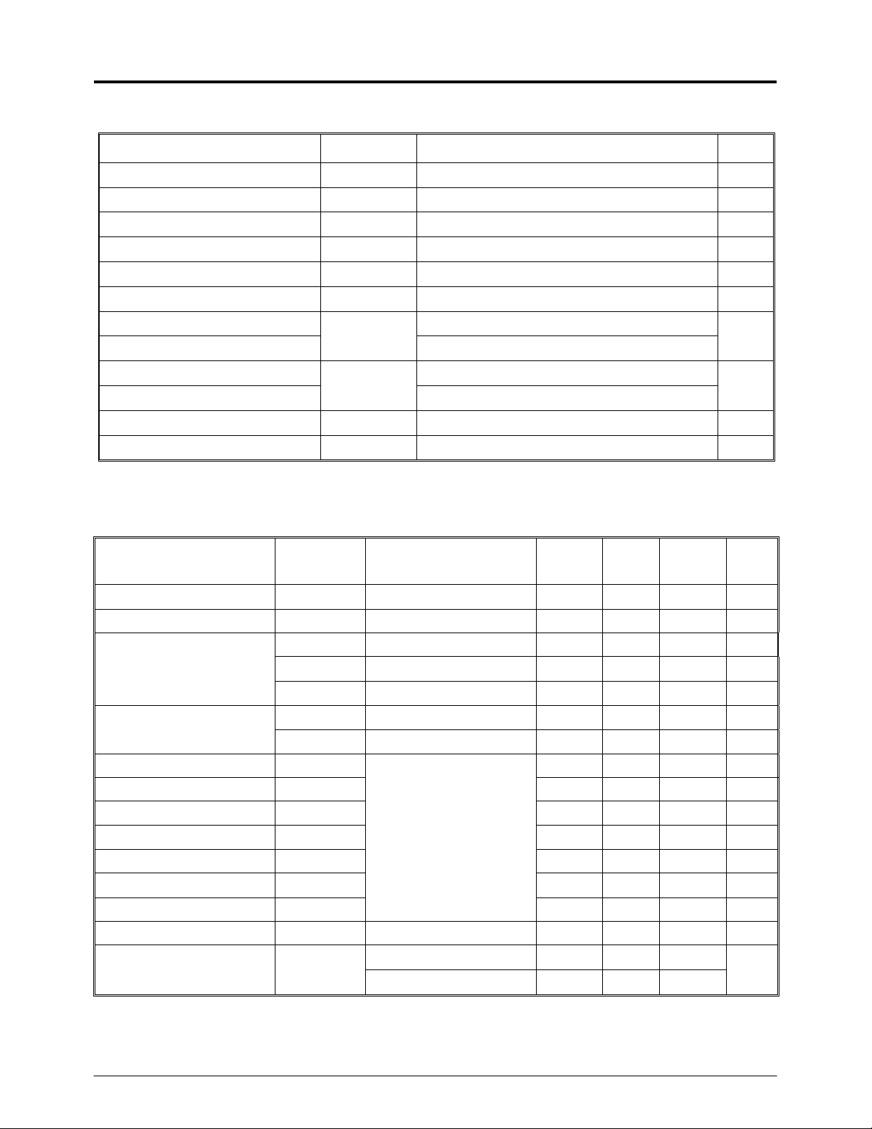
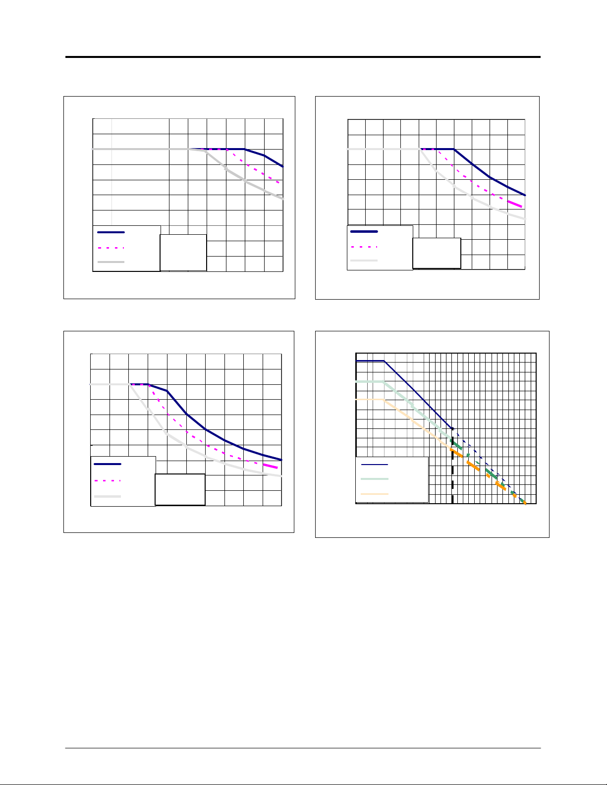
Graphs
100
I
- Duty on PCB
OUT
80
60
(mA)
OUT
I
40
20
0
020406080100
MBI5016CNS
MBI5016CF
MBI5016CP
Ta = 25°C
VDD = 5V
VCE = 1.2V
Tj(max) = 150°C
Duty - Turn on Rate (%)
100
I
- Duty on PCB
OUT
80
60
( mA)
OUT
I
40
MBI5016CNS
20
Graph
0
020406080100
MBI5016CF
MBI5016CP
Ta = 85°C
VDD = 5V
VCE = 1.2V
Tj(max) = 150°C
Duty - Turn on Rate (%)
I
- Duty on PCB
OUT
100
80
60
(mA)
OUT
I
40
20
0
020406080100
MBI5016CNS
MBI5016CF
MBI5016CP
Ta = 55°C
VDD = 5V
VCE = 1.2V
Tj(max) = 150°C
Duty - Turn on Rate (%)
MBI5016 Pd-Ta
1.600
1.400
1.200
1.000
0.800
Pd (W/IC)
0.600
0.400
0.200
0.000
020406080100120140160
MBI5016CNS
MBI5016CF
MBI5016CP
Ta
- 8 -
Page 9

MBI5016-V1.2 16-bit Constant Current LED Sink Driver
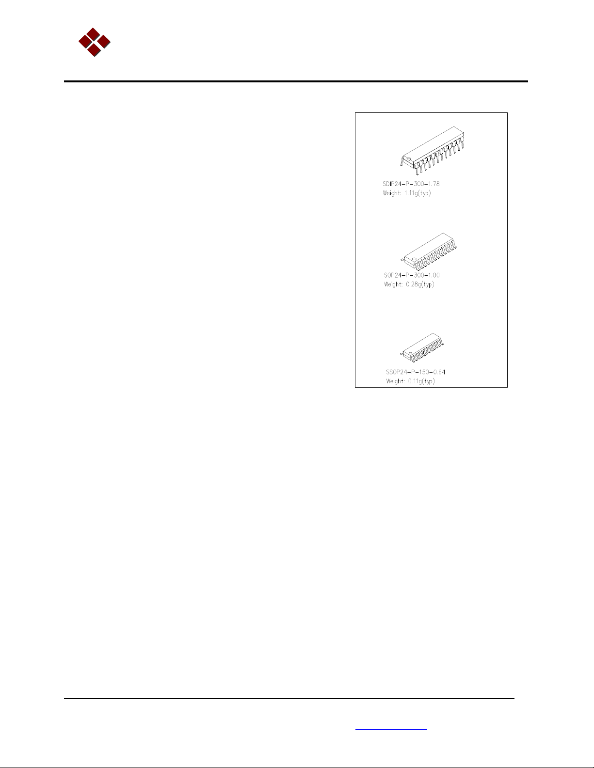
Outline Drawings
MBI5016CNS Outline Drawing
SDIP-24-P-300-1.78
Units: mm
Weight:1.11g(typ)
- 9 -
Page 10
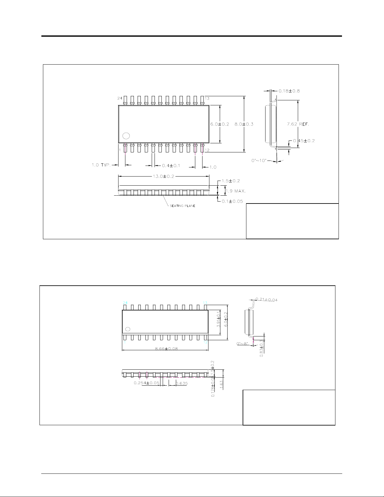
MBI5016-V1.2 16-bit Constant Current LED Sink Driver
MBI5016CF Outline Drawing
MBI5016CP Outline Drawing
SOP24-P-300-1.00
Units: mm
Weight:0.28g(typ)
SSOP24-P-150-0.64
- 10 -
Units: mm
Weight:0.11g(typ)
 Loading...