

Page 1
查询MB90574A供应商
To Top / Lineup / Index
FUJITSU SEMICONDUCTOR
DATA SHEET
DS07-13701-4E
16-bit Proprietary Microcontroller
CMOS
F2MC-16LX MB90570/A Series
MB90573/574/F574/V570/574A/F574A/V570A
DESCRIPTION
■
The MB90570/A series is a general-purpose 16-bit microcontroller developed and designed by Fujitsu for
process control applications in consumer products that require high-speed real time processing. It contains an
2C*2
I
bus interface that allows inter-equipment communication to be implemented readily. This product is well
adapted to car audio equipment, VTR systems, and other equipment and systems.
2
The instruction set of F
sets for high-level languages, extended addressing mode, enhanced multiplication/division instructions, and
enhanced bit manipulation instructions. The microcontroller has a 32-bit accumulator for processing long word
data.
MC-16LX CPU core inherits AT architecture of F2MC*1 family with additional instruction
The MB90570/A series has peripheral resources of an 8/10-bit A/D converter, an 8-bit D/A converter, UART
(SCI), an extended I/O serial interface, an 8/16-bit up/down counter/timer, an 8/16-bit PPG timer, I/O timer (a
16-bit free run timer, an input capture (ICU), an output compare (OCU)).
2
*1: F
MC stands for FUJITSU Flexible Microcontroller.
*2: Purchase of Fujitsu I
components in an I
defined by Philips.
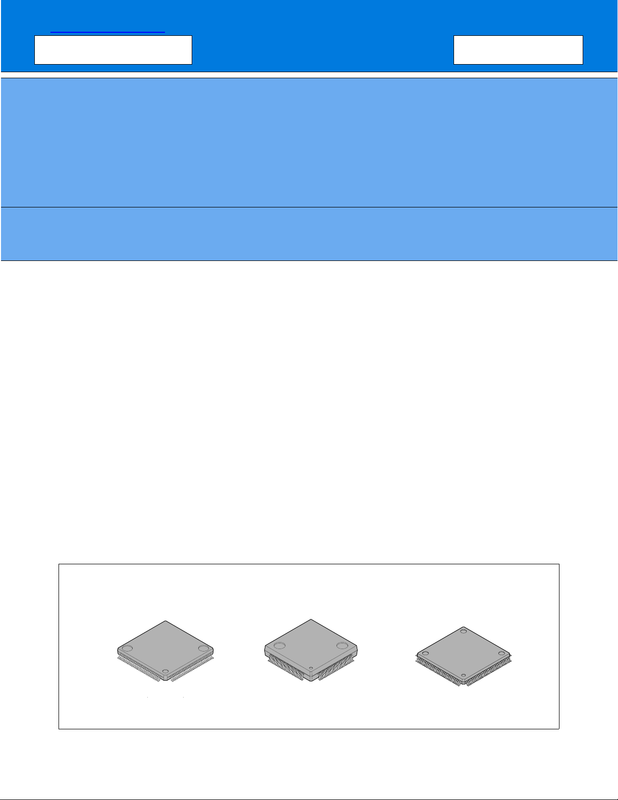
PACKAGE
■
120-pin plastic LQFP
2
C components conveys a license under the Philips I2C Patent Rights to use these
2
C system, provided that the system conforms to the I2C Standard Specification as
120-pin plastic QFP
120-pin plastic LQFP
(FPT-120P-M05)
(FPT-120P-M13)
(FPT-120P-M21)
Page 2

To Top / Lineup / Index
MB90570/A Series
FEATURES
■
•Clock
Embedded PLL clock multiplication circuit
Operating clock (PLL clock) can be selected from 1/2 to 4× oscillation (at oscillation of 4 MHz, 4 MHz to 16 MHz).
Minimum instruction ex ecution time : 62.5 ns (at oscillation of 4 MHz, 4× PLL clock, operation at V
• Maximum memory space
16 Mbytes
• Instruction set optimized for controller applications
Rich data types (bit, byte, word, long word)
Rich addressing mode (23 types)
Enhanced signed multiplication/division instruction and RETI instruction functions
Enhanced precision calculation realized by the 32-bit accumulator
• Instruction set designed for high level language (C) and multi-task operations
Adoption of system stack pointer
Enhanced pointer indirect instructions
Barrel shift instructions
• Program patch function (for two address pointers)
• Enhanced execution speed
4-byte instruction queue
• Enhanced interrupt function
8 levels, 34 factors
• Automatic data transmission function independent of CPU operation
Extended intelligent I/O service function (EI
• Embedded ROM size and types
Mask ROM: 128 Kbytes/256 Kbytes
Flash ROM: 256 Kbytes
Embedded RAM size: 6 Kbytes/10 Kbytes (mask ROM)
10 Kbytes (flash memory)
10 Kbytes (evaluation device)
• Low-power consumption (standby) mode
Sleep mode (mode in which CPU operating clock is stopped)
Stop mode (mode in which oscillation is stopped)
CPU intermittent operation mode
Hardware standby mode
•Process
CMOS technology
• I/O port
General-purpose I/O ports (CMOS): 63 ports
General-purpose I/O ports (with pull-up resistors): 24 ports
General-purpose I/O ports (open-drain): 10 ports
Total: 97 ports
2
OS): Up to 16 channels
of 5.0 V)
CC
(Continued)
2
Page 3

To Top / Lineup / Index
MB90570/A Series
(Continued)
•Timer
Timebase timer/watchdog timer: 1 channel
8/16-bit PPG timer: 8-bit × 2 channels or 16-bit × 1 channel
• 8/16-bit up/down counter/timer: 1 channel (8-bit × 2 channels)
• 16-bit I/O timer
16-bit free run timer: 1 channel
Input capture (ICU): Generates an interrupt request by latching a 16-bit free run timer counter value upon
detection of an edge input to the pin.
Output compare (OCU): Generates an interrupt request and re verse the output lev el upon detection of a match
between the 16-bit free run timer counter value and the compare setting value.
• Extended I/O serial interface: 3 channels
2
•I
C interface (1 channel)
Serial I/O port for supporting Inter IC BUS
• UART0 (SCI), UART1 (SCI)
With full-duplex double buffer
Clock asynchronized or clock synchronized transmission can be selectively used.
• DTP/external interrupt circuit (8 channels)
A module for starting extended intelligent I/O service (EI
by an external input.
• Delayed interrupt generation module
Generates an interrupt request for switching tasks.
• 8/10-bit A/D converter (8 channels)
8/10-bit resolution
Starting by an external trigger input.
Conversion time: 26.3 µs
• 8-bit D/A converter (based on the R-2R system)
8-bit resolution: 2 channels (independent)
Setup time: 12.5 µs
• Clock timer: 1 channel
• Chip select output (8 channels)
An active level can be set.
• Clock output function
2
OS) and generating an external interrupt triggered
3
Page 4
MB90570/A Series
PRODUCT LINEUP
■
To Top / Lineup / Index
Part number
Item
Classification Mask ROM products Flash ROM products Evaluation product
ROM size 128 Kbytes 256 Kbytes None
RAM size 6 Kbytes 10 Kbytes
CPU functions
Ports
UART0 (SCI), UART1 (SCI)
8/10-bit A/D converter
MB90573
Minimum execution time: 62.5 ns (at machine clock of 16 MHz)
Interrupt processing time: 1.5 µs (at machine clock of 16 MHz, minimum value)
General-purpose I/O ports (with pull-up resistor): 24
General-purpose I/O ports (N-ch open-drain output): 10
Clock synchronized transmission (62.5 kbps to 1 Mbps)
Clock asynchronized transmission (1202 bps to 9615 bps)
Transmission can be performed by bi-directional serial transmission or by
master/slave connection.
One-shot conversion mode (converts selected channel only once)
Scan conversion mode (converts two or more successive channels and can
Continuous conversion mode (converts selected channel continuously)
Stop conversion mode (converts selected channel and stop operation repeatedly)
MB90574/A MB90F574/A MB90V570/A
The number of instructions: 340
Instruction bit length: 8 bits, 16 bits
Instruction length: 1 byte to 7 bytes
Data bit length: 1 bit, 8 bits, 16 bits
General-purpose I/O ports (CMOS output): 63
Total: 97
Resolution: 8/10-bit
Number of inputs: 8
program up to 8 channels.)
8/16-bit PPG timer
8/16-bit up/down counter/
timer
16-bit
free run timer
16-bit
I/O timer
4
Output
compare
(OCU)
Input capture
(ICU)
Number of channels: 1 (or 8-bit × 2 channels)
PPG operation of 8-bit or 16-bit
A pulse wave of given intervals and given duty ratios can be output.
Pulse interval: 62.5 ns to 1 µs (at oscillation of 4 MHz, machine clock of 16 MHz)
Number of channels: 1 (or 8-bit × 2 channels)
Event input: 6 channels
8-bit up/down counter/timer used: 2 channels
8-bit re-load/compare function supported: 1 channel
Number of channel: 1
Overflow interrupts
Number of channels: 4
Pin input factor: A match signal of compare register
Number of channels: 2
Rewriting a register value upon a pin input (rising, falling, or both edges)
(Continued)
Page 5
(Continued)
To Top / Lineup / Index
MB90570/A Series
Part number
Item
DTP/external interrupt circuit
Delayed interrupt generation
module
Extended I/O serial interface
2
C interface
I
Timebase timer
8-bit D/A converter
Watchdog timer
Low-power consumption
(standby) mode
MB90573
Started by a rising edge, a falling edge, an “H” level input, or an “L” level input.
External interrupt circuit or extended intelligent I/O service (EI
An interrupt generation module for switching tasks used in real time operating
Clock synchronized transmission (3125 bps to 1 Mbps)
Interrupt interval: 1.024 ms, 4.096 ms, 16.384 ms, 131.072 ms
Reset generation interval: 3.58 ms, 14.33 ms, 57.23 ms, 458.75 ms
Sleep/stop/CPU intermittent operation/clock timer/hardware standby
MB90574/A MB90F574/A MB90V570/A
Number of inputs: 8
2
OS) can be used.
systems.
LSB first/MSB first
Serial I/O port for supporting Inter IC BUS
18-bit counter
(at oscillation of 4 MHz)
8-bit resolution
Number of channels: 2 channels
Based on the R-2R system
(at oscillation of 4 MHz, minimum value)
Process CMOS
Power supply voltage for
operation*
* :Varies with conditions such as the operating frequency. (See section “■ Electrical Characteristics.”)
Assurance for the MB90V570/A is given only for operation with a tool at a power voltage of 4.5 V to 5.5 V, an
operating temperature of 0 to +25°C, and an operating frequency of 1 MHz to 16 MHz.
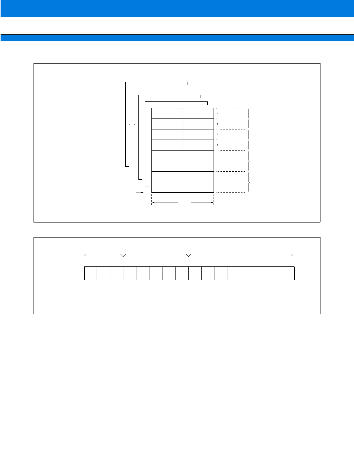
PACKAGE AND CORRESPONDING PRODUCTS
■
Package MB90573 MB90574 MB90F574/A MB90574A
FPT-120P-M05 ×
FPT-120P-M13
FPT-120P-M21 × ×
: Available × : Not available
Note: For more inf ormation about each package, see section “■ Pac kage Dimensions.”
4.5 V to 5.5 V
5
Page 6

To Top / Lineup / Index
MB90570/A Series
DIFFERENCES AMONG PRODUCTS
■
Memory Size
In evaluation with an evaluation product, note the difference between the evaluation product and the product
actually used. The following items must be taken into consideration.
• The MB90V570/A does not have an internal ROM, however, operations equivalent to chips with an internal
ROM can be ev aluated b y using a dedicated development tool, enabling selection of ROM size b y settings of
the development tool.
• In the MB90V570/A, images from FF4000
mapped to bank FE and FF only. (This setting can be changed by configuring the deveolpment tool.)
• In the MB90F574/574/573/F574A/574A, images from FF4000
FF0000
• The products designated with /A are different from those without /A in that they are DTP/externally-interrupted
types which return from standby mode at the ch.0 to ch.1 edge request.
to FF3FFFH to bank FF only.
H
to FFFFFFH are mapped to bank 00, and FE0000H to FF3FFFH to
H
to FFFFFFH are mapped to bank 00, and
H
6
Page 7
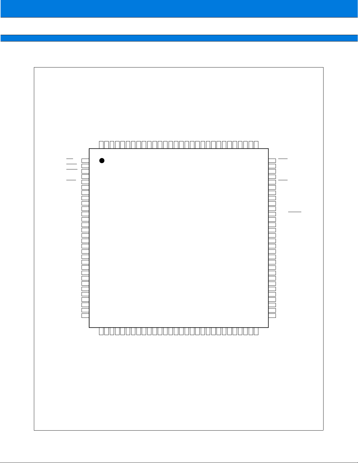
PIN ASSIGNMENT
■
To Top / Lineup / Index
MB90570/A Series
(Top view)
P31/RD
P32/WRL
P33/WRH
P34/HRQ
P35/HAK
P36/RDY
P37/CLK
V
CC
P40/SIN0
P41/SOT0
P42/SCK0
P43/SIN1
P44/SOT1
P45/SCK1
P46/PPG0
P47/PPG1
P50/SIN2
P51/SOT2
P52/SCK2
P53/SIN3
P54/SOT3
P55/SCK3
P56/IN0
P57/IN1
P60/SIN4
P61/SOT4
P62/SCK4
P63/CKOT
P64/OUT0
P65/OUT1
P30/ALE
VSSP27/A23
P26/A22
P25/A21
P24/A20
P23/A19
P22/A18
P21/A17
P20/A16
P17/AD15
P16/AD14
P15/AD13
P14/AD12
P13/AD11
P12/AD10
P11/AD09
P10/AD08
P07/AD07
P06/AD06
P05/AD05
P04/AD04
P03/AD03
P02/AD02
120
119
118
117
116
115
114
113
112
111
110
109
108
107
106
105
104
103
102
101
1
2
3
4
5
6
7
8
9
10
11
12
13
14
15
16
17
18
19
20
21
22
23
24
25
26
27
28
29
30
3132333435363738394041424344454647484950515253545556575859
1009998979695949392
P01/AD01
P00/AD00
VCCX1X0V
SS
91
60
90
89
88
87
86
85
84
83
82
81
80
79
78
77
76
75
74
73
72
71
70
69
68
67
66
65
64
63
62
61
RST
MD0
MD1
MD2
HST
PC3
PC2
PC1
PC0
PB7
PB6/ADTG
PB5/IRQ5
PB4/IRQ4
PB3/IRQ3
PB2/IRQ2
PB1/IRQ1
X0A
X1A
PB0/IRQ0
PA7/SCL
PA6/SDA
PA5/ZIN1
PA4/BIN1
PA3/AIN1/IRQ7
PA2/ZIN0
PA1/BIN0
PA0/AIN0/IRQ6
V
SS
P97/CS7
P96/CS6
P66/OUT2
P67/OUT3
VSSC
P70
P71
P72
DVCCDVSSP73/DA0
P74/DA1
AVCCAVRH
AVRL
(FPT-120P-M05)
(FPT-120P-M13)
(FPT-120P-M21)
AVSSP80/AN0
P81/AN1
P82/AN2
P83/AN3
P84/AN4
P85/AN5
P86/AN6
P87/AN7
VCCP90/CS0
P91/CS1
P92/CS2
P93/CS3
P94/CS4
P95/CS5
7
Page 8
MB90570/A Series
PIN DESCRIPTION
■
Pin no.
Pin name Circuit type Function
LQFP-120 *
QFP-120 *
92,93 X0,X1 A
74,73 X0A,X1A B
89 to 87 MD0 to MD2 C
90 RST C
86 HST C
95 to 102 P00 to P07 D
103 to 110 P10 to P17 D
111 to 118 P20 to P27 E
120 P30 E
1
2
AD00 to AD07
AD08 to AD15
A16 to A23
ALE
1P31 E
RD
2P32 E
WRL
3P33 E
WRH
4P34 E
HRQ
5P35 E
HAK
6P36 E
RDY
To Top / Lineup / Index
High speed oscillator input pins
Low speed oscillator input pins
These are input pins used to designate the operating mode. They should
be connected directly to Vcc or Vss.
Reset input pin
Hardware standby input pin
In single chip mode, these are general purpose I/O pins. When set for
input, they can be set by the pull-up resistance setting register (RDR0).
When set for output, this setting will be invalid.
In external bus mode, these pins function as address low output/data low
I/O pins.
In single chip mode, these are general purpose I/O pins. When set for
input, they can be set by the pull-up resistance setting register (RDR1).
When set for output, the setting will be invalid.
In external bus mode, these pins function as address middle output/data
high I/O pins.
In single chip mode this is a general-purpose I/O port.
In external bus mode, these pins function as address high output pins.
In single chip mode this is a general-purpose I/O port.
In external bus mode, this pin functions as the address latch enable signal
output pin.
In single chip mode this is a general-purpose I/O port.
In external bus mode, this pin functions as the read strobe signal output
pin.
In single chip mode this is a general-purpose I/O port.
In external bus mode, this pin functions as the data bus lower 8-bit write
strobe signal output pin.
In single chip mode this is a general-purpose I/O port.
In external bus mode, this pin functions as the data bus upper 8-bit write
strobe signal output pin.
In single chip mode this is a general-purpose I/O port.
In external bus mode, this pin functions as the hold request signal input
pin.
In single chip mode this is a general-purpose I/O port.
In external bus mode, this pin functions as the hold acknowledge signal
output pin.
In single chip mode this is a general-purpose I/O port.
In external bus mode, this pin functions as the ready signal input pin.
.
*1: FPT-120P-M05
*2: FPT-120P-M13
8
FPT-120P-M21
,
(Continued)
Page 9
Pin no.
Pin name Circuit type Function
LQFP-120 *
QFP-120 *
1
2
7P37 E
CLK
9P40 F
SIN0
10 P41 F
SOT0
11 P42 F
SCK0
12 P43 F
SIN1
13 P44 F
SOT1
14 P45 F
SCK1
15,16 P46,P47 F
PPG0,PPG1
17 P50 E
SIN2
To Top / Lineup / Index
MB90570/A Series
In single chip mode this is a general-purpose I/O port.
In external bus mode, this pin functions as the clock (CLK) signal output
pin.
In single chip mode this is a general-purpose I/O port. It can be set to open
drain by the ODR4 register.
This is also the UART ch.0 serial data input pin. While UART ch.0 is in
input operation, this input signal is in continuous use, and therefore the
output function should only be used when needed. If shared by output
from other functions, this pin should be output disabled during SIN
operation.
In single chip mode this is a general-purpose I/O port. It can be set to open
drain by the ODR4 register.
This is also the UART ch.0 serial data output pin. This function is valid
when UART ch.0 is enabled for data output.
In single chip mode this is a general-purpose I/O port. It can be set to open
drain by the ODR4 register.
This is also the UART ch.0 serial clock I/O pin. This function is valid when
UART ch.0 is enabled for clock output.
In single chip mode this is a general-purpose I/O port. It can be set to
open-drain by the ODR4 register.
This is also the UART ch.1 serial data input pin. While UART ch.1 is in
input operation, this input signal is in continuous use, and therefore the
output function should only be used when needed. If shared by output
from other functions, this pin should be output disabled during SIN
operation.
In single chip mode this is a general-purpose I/O port. It can be set to
opendrain by the ODR4 register.
This is also the UART ch.1 serial data output pin. This function is valid
when UART ch.1 is enabled for data output.
In single chip mode this is a general-purpose I/O port. It can be set to open
drain by the ODR4 register.
This is also the UART ch.1 serial clock I/O pin. This function is valid when
UART ch.1 is enabled for clock output.
In single chip mode this is a general-purpose I/O port. It can be set to open
drain by the ODR4 register.
These are also the PPG0, 1 output pins. This function is valid when PPG0,
1 output is enabled.
In single chip mode this is a general-purpose I/O port.
This is also the I/O serial ch.0 data input pin. During serial data input, this
input signal is in continuous use, and therefore the output function should
only be used when needed.
*1: FPT-120P-M05
*2: FPT-120P-M13
FPT-120P-M21
,
(Continued)
9
Page 10
MB90570/A Series
Pin no.
Pin name Circuit type Function
LQFP-120 *
QFP-120 *
18 P51 E
19 P52 E
20 P53 E
21 P54 E
22 P55 E
23,24 P56,P57 E
25 P60 F
26 P61 F
27 P62 F
28 P63 F
*1: FPT-120P-M05
*2: FPT-120P-M13
1
2
SOT2
SCK2
SIN3
SOT3
SCK3
IN0,IN1
SIN4
SOT4
SCK4
CKOT
FPT-120P-M21
,
To Top / Lineup / Index
In single chip mode this is a general-purpose I/O port.
This is also the I/O serial ch.0 data output pin. This function is valid when
serial ch.0 is enabled for serial data output.
In single chip mode this is a general-purpose I/O port .
This is also the I/O serial ch.0 clock I/O pin. This function is valid when
serial ch.0 is enabled for serial data output.
In single chip mode this is a general-purpose I/O port.
This is also the I/O serial ch.1 data input pin. During serial data input, this
input signal is in continuous use, and therefore the output function should
only be used when needed.
In single chip mode this is a general-purpose I/O port.
This is also the I/O serial ch.1 data output pin. This function is valid when
serial ch.1 is enabled for serial data output.
In single chip mode this is a general-purpose I/O port.
This is also the I/O serial ch.1 clock I/O pin. This function is valid when
serial ch.1 is enabled for serial data output.
In single chip mode this is a general-purpose I/O port.
These are also the input capture ch.0/1 trigger input pins. During input
capture signal input on ch.0/1 this function is in continuous use, and
therefore the output function should only be used when needed.
In single chip mode this is a general-purpose I/O port. When set for input
it can be set by the pull-up resistance register (RDR6). When set for
output this setting will be invalid.
This is also the I/O serial ch.2 data input pin. During serial data input this
function is in continuous use, and therefore the output function should
only be used when needed.
In single chip mode this is a general-purpose I/O port. When set for input
it can be set by the pull-up resistance register (RDR6). When set for
output this setting will be invalid.
This is also the I/O serial ch.2 data output pin. This function is valid when
serial ch.2 is enabled for serial data output.
In single chip mode this is a general-purpose I/O port. When set for input
it can be set by the pull-up resistance register (RDR6). When set for
output this setting will be invalid.
This is also the I/O serial ch.2 serial clock I/O pin. This function is valid
when serial ch.2 is enabled for serial data output.
In single chip mode this is a general-purpose I/O port. When set for input
it can be set by the pull-up resistance register (RDR6). When set for
output this setting will be invalid.
This is also the clock monitor output pin. This function is valid when cloc k
monitor output is enabled.
(Continued)
10
Page 11
Pin no.
Pin name Circuit type Function
LQFP-120 *
QFP-120 *
1
2
29 to 32 P64 to P67 F
OUT0 to
OUT3
35 to 37 P70 to P72 E
40,41 P73,P74 I
DA0,DA1
46 to 53 P80 to P87 K
AN0 to AN7
55 to 62 P90 to P97 E
CS0 to CS7
34 C G
64 PA0 E
AIN0
IRQ6
65 PA1 E
BIN0
66 PA2 E
ZIN0
67 PA3 E
AIN1
IRQ7
68 PA4 E
BIN1
69 PA5 E
ZIN1
To Top / Lineup / Index
MB90570/A Series
In single chip mode these are general-purpose I/O ports. When set for
input they can be set by the pull-up resistance register (RDR6). When set
for output this setting will be invalid.
These are also the output compare ch.0 to ch.3 event output pins. This
function is valid when the respective channel(s) are enabled for output.
These are general purpose I/O ports.
These are general purpose I/O ports.
These are also the D/A converter ch.0,1 analog signal output pins.
These are general purpose I/O ports.
These are also A/D converter analog input pins. This function is valid
when analog input is enabled.
These are general purpose I/O ports.
These are also chip select signal output pins. This function is valid when
chip select signal output is enabled.
This is the power supply stabilization capacitor pin. It should be
connected externally to an 0.1 µF ceramic capacitor. Note that this is
not required on the FLASH model (MB90F574/A) and MB90574A.
This is a general purpose I/O port.
This pin is also used as count clock A input for 8/16-bit up-down counter
ch.0.
This pin can also be used as interrupt request input ch. 6.
This is a general purpose I/O port.
This pin is also used as count clock B input for 8/16-bit up-down counter
ch.0.
This is a general purpose I/O port.
This pin is also used as count clock Z input for 8/16-bit up-down counter
ch.0.
This is a general purpose I/O port.
This pin is also used as count clock A input for 8/16-bit up-down counter
ch.1.
This pin can also be used as interrupt request input ch.7.
This is a general purpose I/O port.
This pin is also used as count clock B input for 8/16-bit up-down counter
ch.1.
This is a general purpose I/O port.
This pin is also used as count clock Z input for 8/16-bit up-down counter
ch.1.
*1: FPT-120P-M05
*2: FPT-120P-M13
FPT-120P-M21
,
(Continued)
11
Page 12
MB90570/A Series
(Continued)
Pin no.
Pin name Circuit type Function
LQFP-120 *
QFP-120 *
70 PA6 L
71 PA7 L
72,
75 to 79
80 PB6 E
81 PB7 E
82 to 85 PC0 to PC3 E
8,54,94 V
33,63,
91,119
42 AV
43 AVRH J
44 AVRL H
45 AV
38 DV
39 DV
1
2
SDA
SCL
PB0,
PB1 to PB5
IRQ0,
IRQ1 to IRQ5
ADTG
CC
V
SS
CC
SS
CC
SS
Power
supply
Power
supply
To Top / Lineup / Index
This is a general purpose I/O port.
This pin is also used as the data I/O pin for the 12C interface. This
function is valid when the 1
2
the 1
C interface is operating this port's output level should be set to
Hi-Z level (high impedance setting: PDRA=1).
This is a general purpose I/O port.
This pin is also used as the clock I/O pin for the 12C interface. This
function is valid when the 1
2
the 1
C interface is operating this port's output level should be set to
Hi-Z level (high impedance setting: PDRA=1).
E
H
H
H
H
These are general-purpose I/O ports.
These pins are also the external interrupt input pins. IRQ0, 1 are
enabled for both rising and falling edge detection, and therefore cannot
be used for recovery from STOP status for MB90V570, MB90F574,
MB90573 and MB90574. However, IRQ0, 1 can be used for recovery
from STOP status for MB90V570A, MB90F574A and MB90574A.
This is a general purpose I/O port.
This is also the A/D converter external trigger input pin. While the A/D
converter is in input operation, this input signal is in continuous use, and
therefore the output function should only be used when needed.
This is a general purpose I/O port.
These are general purpose I/O ports.
These are power supply (5V) input pins.
These are power supply (0V) input pins.
This is the analog macro (D/A, A/D etc.) Vcc power supply input pin.
This is the A/D converter Vref+ input pin. The input voltage should not
exceed Vcc.
This is the A/D converter Vref-input pin. The input voltage should not
belower than Vss.
This is the analog macro (D/A, A/D etc.) Vss power supply input pin.
This is the D/A converter Vref input pin. The input voltage should not
exceed Vcc..
This is the D/A converter GND power supply pin. It should be set to Vss
equivalent potential.
2
C interface is enabled for operation. While
2
C interface is enabled for operation. While
*1: FPT-120P-M05
*2: FPT-120P-M13
12
FPT-120P-M21
,
Page 13
MB90570/A Series
I/O CIRCUIT TYPE
■
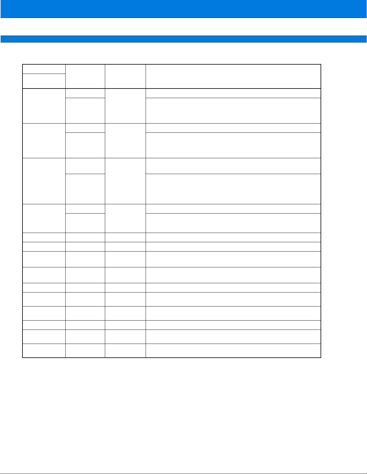
Type Circuit Remarks
A • Oscillator circuit
X1
X0
Standby control signal
B • Oscillator circuit
X1A
Oscillator recovery resistance for high
speed= approx. 1M
Oscillator recovery resistancer for low
speed =approx. 1MΩ
To Top / Lineup / Index
Ω
X0A
Standby control signal
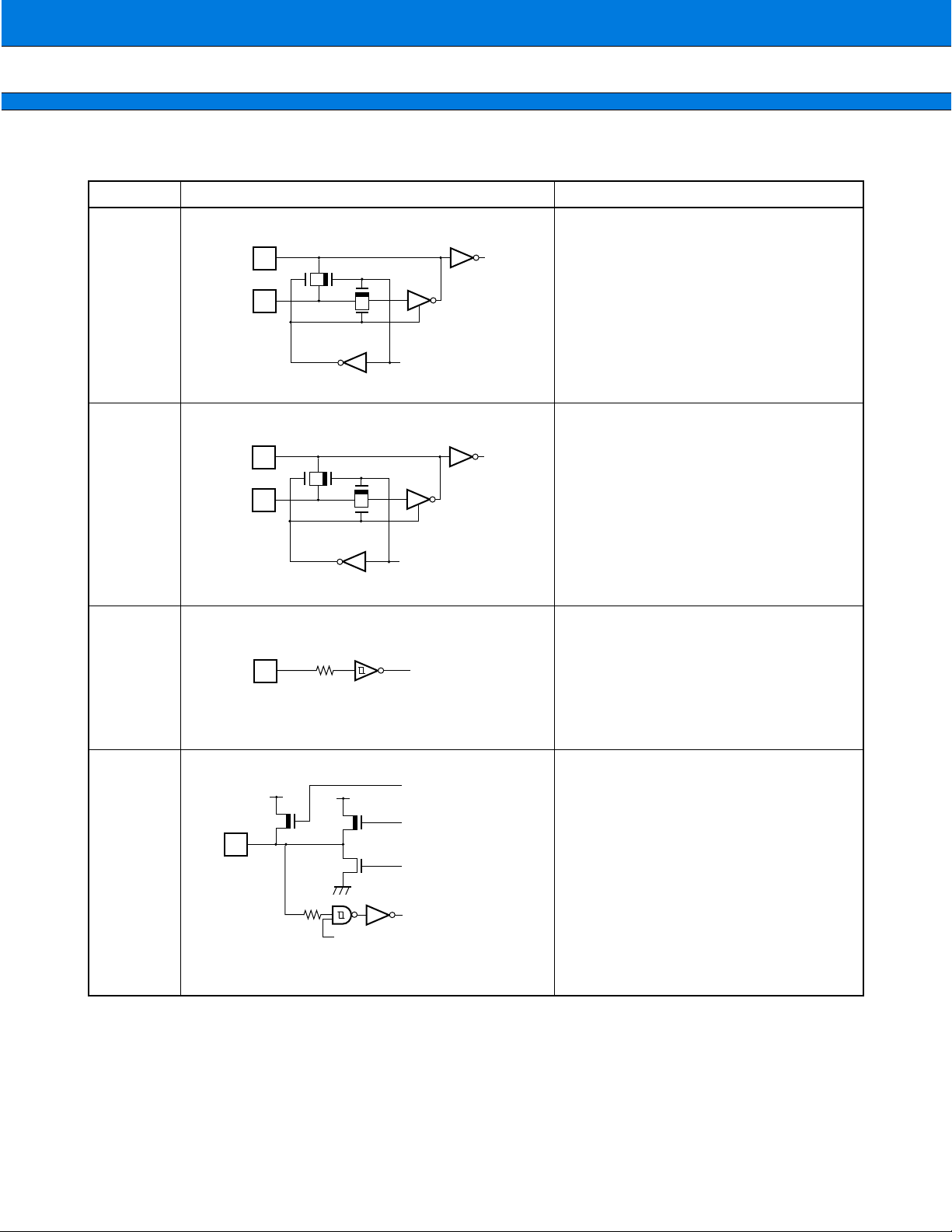
C • Hysteresis input pin
Resistance value=approx. 50kΩ(typ.)
R
Hysteresis input
D • CMOS hystersis input pin with input pull-
V
CC
V
P-ch
Selective signal either
with a pull-up resistor or
CC
without it.
P-ch
up control
• CMOS level output.
• CMOS hystersis input
(Includes input shutoff standby control
function)
= 4 mA
I
OL
N-ch
R
Standby control for input interruption
Hysteresis input
• Pull-up resistance value=
approx.50kΩ(typ.)
I
= 4mA
OL
(Continued)
13
Page 14
MB90570/A Series
Type Circuit Remarks
E • CMOS hysteresis input/output pin.
IOL = 4 mA
V
CC
P-ch
N-ch
R
Standby control for input interruption
Hysteresis input
• CMOS level output
• CMOS hysteresis input
(Includes input shutoff standby control
function)
I
= 4mA
OL
To Top / Lineup / Index
F • CMOS hysteresis input/output pin.
V
CC
P-ch
• CMOS level output
• CMOS hysteresis input
(Includes input shutoff standby control
function)
= 10mA (Large current port)
I
N-ch
R
= 10 mA
I
OL
G • C pin output
V
Standby control for input interruption
CC
Hysteresis input
OL
(capacitance connector pin).
P-ch
N-ch
H • Analog power supply protector
V
CC
On the MB90F574 this pin is not
connected (NC).
circuit.
P-ch
AVP
N-ch
14
I • CMOS hysteresis input/output
V
CC
P-ch
• Analog output/CMOS output
dual-function pin ( CMOS output is not
available during analog output.)
(Analog output priority : DAE = 1)
= 4 mA
I
OL
N-ch
R
Standby control for input interruption
Hysteresis input
DAO
• Includes input shutoff standby control
function.
I
= 4mA
OL
(Continued)
Page 15
To Top / Lineup / Index
MB90570/A Series
Type Circuit Remarks
J • A/D converter ref+ power supply input
V
CC
P-ch
N-ch
ANE
AVR
ANE
P-ch
N-ch
pin(AVRH), with power supply
protector circuit.
K • CMOS hysteresis input /analog input
V
CC
P-ch
dual-function pin.
• CMOS output
• Includes input shutoff function at input
N-ch
R
Standby control for input interruption
I
= 4 mA
OL
L • Hysteresis input
V
CC
Hysteresis input
Analog input
N-ch
shutoff standby.
• N-ch open-drain output
• Includes input shutoff standby control
function.
I
= 4mA
OL
= 4 mA
I
OL
N-ch
R
Hysteresis input
Standby control for input interruption
15
Page 16
To Top / Lineup / Index
MB90570/A Series
HANDLING DEVICES
■
1. Make Sure that the Voltage not Exceed the Maximum Rating (to Avoid a Latch-up).
In CMOS ICs, a latch-up phenomenon is caused when an voltage exceeding VCC or an voltage below VSS is
applied to input or output pins or a voltage exceeding the rating is applied across V
When a latch-up is caused, the power supply current may be dramatically increased causing resultant thermal
break-down of devices. To avoid the latch-up, make sure that the voltage not exceed the maximum rating.
and VSS.
CC
In turning on/turning off the analog power supply, make sure the analog power voltage (AV
analog input voltages not exceed the digital voltage (V
CC
).
, AVRH, DVCC) and
CC
2. Connection of Unused Pins
Leaving unused pins open may result in abnormal operations. Clamp the pin level by connecting it to a pull-up
or a pull-down resistor.
3. Notes on Using External Clock
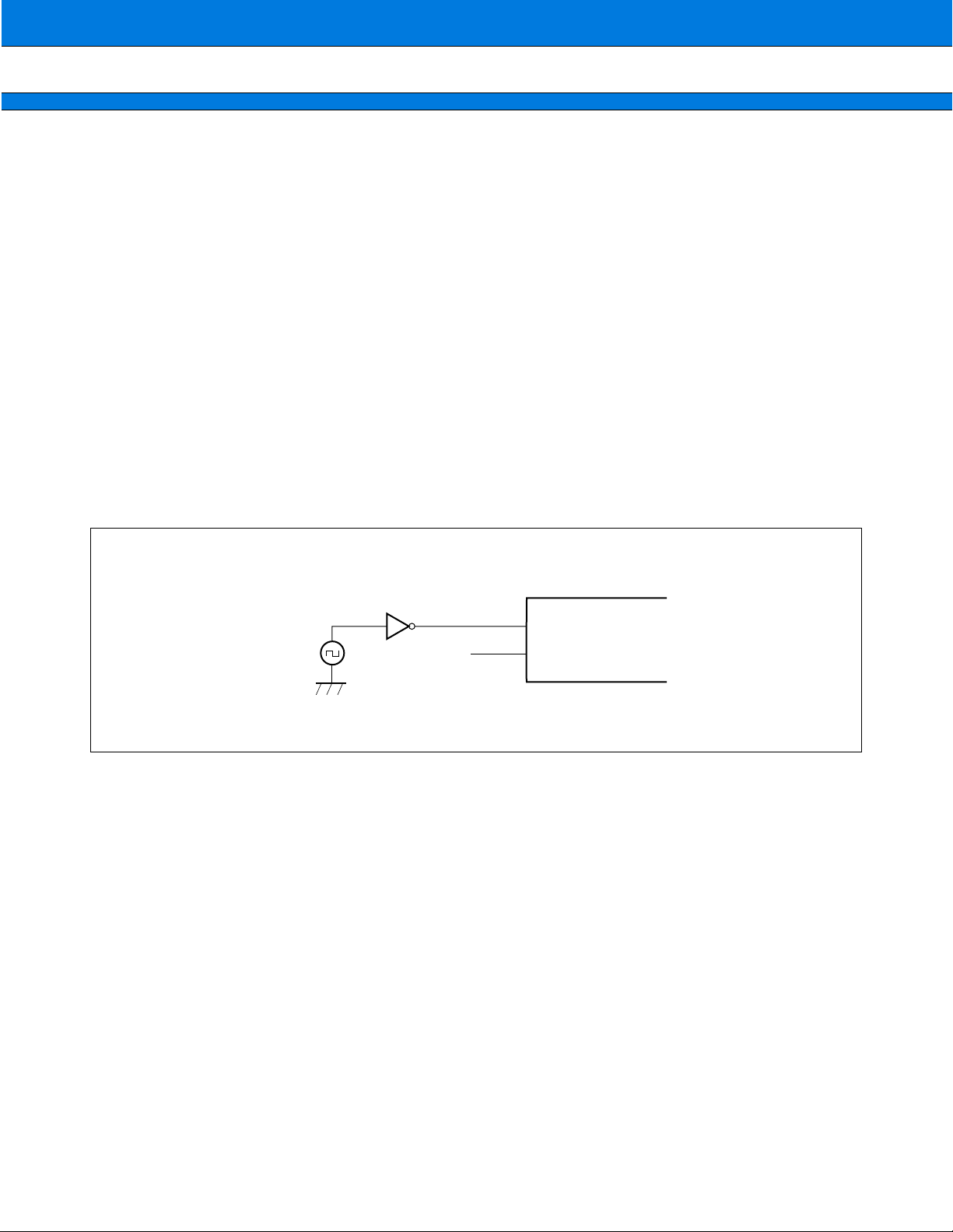
In using the external clock, drive X0 pin only and leave X1 pin unconnected.
Using external clock
•
X0
Open
X1
MB90570/A series
4. Power Supply Pins
In products with multiple VCC or VSS pins, the pins of a same potential are internally connected in the device to
avoid abnormal operations including latch-up. However, connect the pins external power and ground lines to
lower the electro-magnetic emission level and abnormal operation of strobe signals caused by the rise in the
ground level, and to conform to the total current rating.
Make sure to connect V
It is recommended to provide a bypass capacitor of around 0.1 µF between V
5. Crystal Oscillator Circuit
Noises around X0 or X1 pins may be possible causes of abnormal operations. Make sure to provide bypass
capacitors via shortest distance from X0, X1 pins, crystal oscillator (or ceramic resonator) and ground lines, and
make sure, to the utmost effort, that lines of oscillation circuit not cross the lines of other circuits.
It is highly recommended to provide a printed circuit board art work surrounding X0 and X1 pins with an grand
area for stabilizing the operation.
16
and VSS pins via lowest impedance to power lines.
CC
and VSS pin near the device.
CC
Page 17

To Top / Lineup / Index
MB90570/A Series
6. Turning-on Sequence of Power Supply to A/D Conv erter and Analog Inputs
Make sure to turn on the A/D converter power supply, D/A converter power supply (AVCC, AVRH, AVRL, DVCC,
DV
) and analog inputs (AN0 to AN7) after turning-on the digital power supply (VCC).
SS
Turn-off the digital power after turning off the A/D converter supply and analog inputs. In this case, make sure
that the voltage not exceed AVRH or AV
is acceptable).
7. Connection of Unused Pins of A/D Converter
Connect unused pins of A/D converter and those of D/A converter to AVCC = VCC, AVSS = AVRH = DVCC = VSS.
8. N.C. Pin
The N.C. (internally connected) pin must be opened for use.
9. Notes on Energization
(turning on/off the analog and digital power supplies simultaneously
CC
To prevent the internal regulator circuit from malfunctioning, set the voltage rise time during energization at 50
or more µs (0.2 V to 2.7 V).
10. Initialization
In the device, there are internal registers which is initialized only by a power-on reset. To initialize these registers
turning on the power again.
17
Page 18
MB90570/A Series
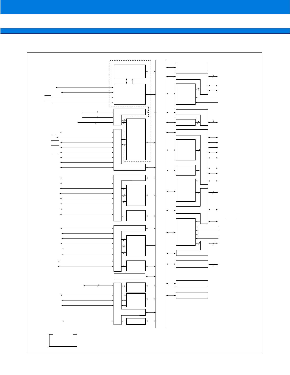
BLOCK DIAGRAM
■
To Top / Lineup / Index
X0, X1
X0A, X1A
RST
HST
P00/AD00 to P07/AD07
P10/AD08 to P17/AD15
P20/A16 to P27/A23
P30/ALE
P31/RD
P32/WRL
P33/WRH
P34/HRQ
P35/HAK
P36/RDY
P37/CLK
P40/SIN0
P41/SOT0
P42/SCK0
P43/SIN1
P44/SOT1
P45/SCK1
P46/PPG0
P47/PPG1
P50/SIN2
P51/SOT2
P52/SCK2
P53/SIN3
P54/SOT3
P55/SCK3
P56/IN0
P57/IN1
Main clock
Sub clock
2
F
MC–16LX
CPU
Clock control
block
(including timebase
timer)
8
8
8
Port 0, 1, 2
16
8
2
External bus
interface
6
Port 3
Port 4
2
UART0
2
UART1
2
8/16-bit
PPG timer
Port 5
2
2
SIO × 2 ch
2
2
Input capture
Internal data bus
(SCI),
(SCI)
ch.0
(ICU)
Interrupt controller
Port 7
8-bit
D/A
converter
×
2 ch.
Port 9
Chip select
output
Port A
8/16-bit up/down
counter/timer
I2C bus
DTP/
external
interrupt
circuit
8 ch.
×
Port B
8/10-bit
A/D converter
×
8 ch.
Port 8
Port C
3
P70 to P72
2
6
2
6
8
P73/DA0
P74/DA1
DV
CC
DV
SS
88
P90/CS0 to P97/CS7
PA1/BIN0
PA2/ZIN0
PA3/AIN1/IRQ7
PA4/BIN1
PA5/ZIN1
PA6/SDA
PA7/SCL
PA0/AIN0/IRQ6
6
PB0/IRQ0 to
PB5/IRQ5
PB7
PB6/ADTG
AVRL
AVRH
AV
CC
AV
SS
8
P80/AN0 to
P87/AN7
4
PC0 to PC3
18
P64/OUT0 to P67/OUT3
P60/SIN4
P61/SOT4
P62/SCK4
P63/SKOT
Other pins
MD0 to MD2,
, V
C, V
CC
SS
16-bit free run timer
4
4
Output
compare
(OCU)
SIO × 1 ch.
Port 6
Clock output
RAM
ROM
P00 to P07 (8 ports): Provided with a register optional input pull-up resistor
P10 to P17 (8 ports): Provided with a register optional input pull-up resistor
P40 to P47 (8 ports): Heavy-current (I
P60 to P67 (8 ports): Provided with a register optional input pull-up resistor
= 10 mA) por
OL
Page 19
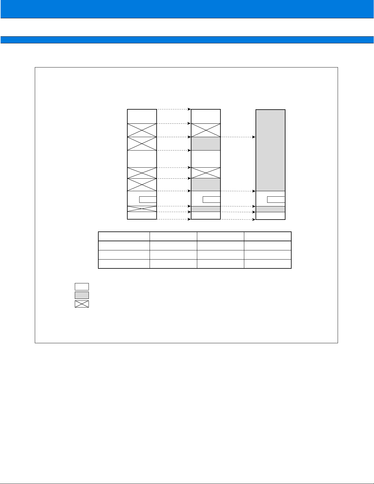
MEMORY MAP
■
FFFFFF
H
Address #1
FC0000
H
010000
H
Address #2
004000
H
Internal ROM
Single chip mode
A mirror function is
supported.
ROM area ROM area
ROM area
(image of
bank FF)
external bus mode
A mirror function
is supported.
ROM area
(image of
bank FF)
To Top / Lineup / Index
MB90570/A Series
External ROM
external bus mode
Address #3
000100
0000C0
000000
Register
RAM RAM RAM
H
H
H
Register
PeripheralPeripheral Peripheral
Register
Part number Address #1* Address #2 * Address #3 *
MB90573 FE0000
MB90574/A FC0000
MB90F574/A FC0000
: Internal access memory
: External access memory
: Inhibited area
*: Addresses #1, #2 and #3 are unique to the product type.
H
H
H
004000
004000
004000
H
H
H
001800
002900
002900
H
H
H
Note: The ROM data of bank FF is reflected in the upper address of bank 00, realizing effectiv e use of the C compiler
small model. The lower 16-bit of bank FF and the lower 16-bit of bank 00 is assigned to the same address ,
enabling reference of the table on the ROM without stating “far”.
For example, if an attempt has been made to access 00C000
, the contents of the ROM at FFC000H are
H
accessed actually . Since the ROM area of the FF bank exceeds 48 Kb ytes, the whole area cannot be reflected
in the image for the 00 bank. The ROM data at FF4000
for 00400
to FFFFFF
to 00FFFFH. Thus, it is recommended that the ROM data table be stored in the area of FF4000H
H
.
H
to FFFFFFH looks, therefore, as if it w ere the image
H
19
Page 20
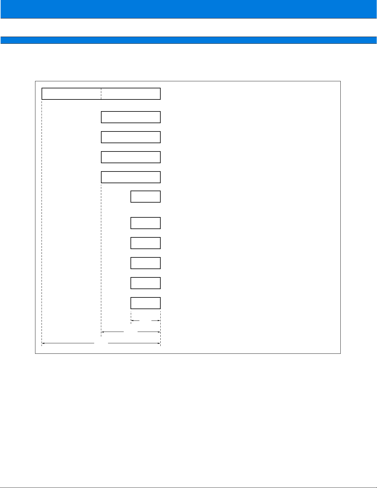
MB90570/A Series
2
F
MC-16LX CPU PROGRAMMING MODEL
■
• Dedicated registers
To Top / Lineup / Index
AH AL
USP
SSP
PS
PC
DPR
PCB
DTB
USB
: Accumlator (A)
Dual 16-bit register used for storing results of calculation etc. The two 16-bit
registers can be combined to be used as a 32-bit register.
: User stack pointer (USP)
The 16-bit pointer indicating a user stack address.
: System stack pointer (SSP)
The 16-bit pointer indicating the status of the system stack address.
: Processor status (PS)
The 16-bit register indicating the system status.
: Program counter (PC)
The 16-bit register indicating storing location of the current instruction code.
: Direct page register (DPR)
The 8-bit register indicating bit 8 through 15 of the operand address in the short
direct addressing mode.
: Program bank register (PCB)
The 8-bit register indicating the program space.
: Data bank register (DTB)
The 8-bit register indicating the data space.
: User stack bank register (USB)
The 8-bit register indicating the user stack space.
32-bit
16-bit
SSB
ADB
8-bit
: System stack bank register (SSB)
The 8-bit register indicating the system stack space.
: Additional data bank register (ADB)
The 8-bit register indicating the additional data space.
20
Page 21
• General-purpose registers
To Top / Lineup / Index
MB90570/A Series
Maximum of 32 banks
+ (RP × 10H )
000180
H
• Processor status (PS)
ILM RP CCR
bit 15 bit 14 bit 13 bit 12 bit 11 bit 10 bit 9 bit 8 bit 7 bit 6 bit 5 bit 4 bit 3 bit 2 bit 1 bit 0
PS
ILM2 B4ILM1 ILM0 B3 B2 B1 B0 — I S T N Z V C
R7
R5
R3
R1
RW3
RW2
RW1
RW0
16-bit
R6
R4
R2
R0
RW7
RL3
RW6
RW5
RL2
RW4
RL1
RL0
Initial value
— : Reserved
X : Undefined
00 000000 10XXXXX
—
21
Page 22
MB90570/A Series
I/O MAP
■
To Top / Lineup / Index
Address
000000
000001
000002
000003
000004
000005
000006
000007
000008
000009
00000A
00000B
00000C
00000D
to
00000F
000010
000011
000012
000013
000014
000015
000016
000017
000018
000019
00001A
00001B
00001C
00001D
00001E
00001F
000020
000021
Abbreviated
register
Register name
name
PDR0 Port 0 data register R/W Port 0 X X XXXXXX
H
PDR1 Port 1 data register R/W Port 1 X X XXXXXX
H
PDR2 Port 2 data register R/W Port 2 X X XXXXXX
H
PDR3 Port 3 data register R/W Port 3 X X XXXXXX
H
PDR4 Port 4 data register R/W Port 4 X X XXXXXX
H
PDR5 Port 5 data register R/W Port 5 X X XXXXXX
H
PDR6 Port 6 data register R/W Port 6 X X XXXXXX
H
PDR7 Port 7 data register R/W Port 7 – – –XXXXX
H
PDR8 Port 8 data register R/W Port 8 X X XXXXXX
H
PDR9 Port 9 data register R/W Port 9 X X XXXXXX
H
PDRA Port A data register R/W Port A XXXXX X X X
H
PDRB Port B data register R/W Port B XXXXX X X X
H
PDRC Port C data register R/W Port C XXXXXX X X
H
H
Read/
write
Resource name Initial value
(Disabled)
H
DDR0 Port 0 direction register R/W Port 0 0 0 0 0 0 0 0 0
H
DDR1 Port 1 direction register R/W Port 1 0 0 0 0 0 0 0 0
H
DDR2 Port 2 direction register R/W Port 2 0 0 0 0 0 0 0 0
H
DDR3 Port 3 direction register R/W Port 3 0 0 0 0 0 0 0 0
H
DDR4 Port 4 direction register R/W Port 4 0 0 0 0 0 0 0 0
H
DDR5 Port 5 direction register R/W Port 5 0 0 0 0 0 0 0 0
H
DDR6 Port 6 direction register R/W Port 6 0 0 0 0 0 0 0 0
H
DDR7 Port 7 direction register R/W Port 7 – – – 0 0 0 0 0
H
DDR8 Port 8 direction register R/W Port 8 0 0 0 0 0 0 0 0
H
DDR9 Port 9 direction register R/W Port 9 0 0 0 0 0 0 0 0
H
DDRA Port A direction register R/W Port A 0 0 0 0 0 0 0 0
H
DDRB Port B direction register R/W Port B 0 0 0 0 0 0 0 0
H
DDRC Port C direction register R/W Port C 0 0 0 0 0 0 0 0
H
ODR4 Port 4 output pin register R/W Port 4 0 0 0 0 0 0 0 0
H
Port 8,
ADER Analog input enable register R/W
H
8/10-bit
11111111
A/D converter
H
SMR0 Serial mode register 0 R/W
H
SCR0 Serial control register 0 R/W 0 0 0 0 0 1 0 0
H
(Disabled)
UART0
(SCI)
00000000
B
B
B
B
B
B
B
B
B
B
B
B
B
B
B
B
B
B
B
B
B
B
B
B
B
B
B
B
B
B
22
(Continued)
Page 23
To Top / Lineup / Index
MB90570/A Series
Address
000022
000023
000024
000025
000026
000027
000028
000029
00002A
00002B
to
00002F
000030
000031
000032
000033
000034
000035
000036
000037
000038
000039
00003A
00003B
00003C
00003D
00003E
00003F
000040
000041
Abbreviated
register
name
SIDR0/
H
SODR0
Register name
Serial input data register 0/
serial output data register 0
Read/
write
R/W
Resource name Initial value
UART0
XXXXXXXX
(SCI)
SSR0 Serial status register 0 R/W 00001–00
H
SMR1 Serial mode register 1 R/W
H
SCR1 Serial control register 1 R/W 00000100
H
00000000
UART1
SIDR1/
H
SODR1
SSR1 Serial status register 1 R/W 00001–00
H
CDCR0
H
H
CDCR1
H
H
Serial input data register 1/
serial output data register 1
Communications prescaler control
register 0
(Disabled)
Communications prescaler control
register 1
R/W XXXXXXXX
(SCI)
Communications
R/W
prescaler
0–––1111
register 0
Communications
R/W
prescaler
0–––1111
register 0
(Disabled)
H
H
H
H
ENIR DTP/interrupt enable register R/W
EIRR DTP/interrupt factor register R/W XXXXXXXX
DTP/external
interrupt circuit
00000000
00000000
ELVR Request level setting register R/W
H
H
00000000
(Disabled)
H
ADCS1
H
ADCS2
H
ADCR1 A/D data register lower digits R XXXXX X X X
H
ADCR2 A/D data register upper digits R 0 0 0 0 1 – XX
H
DADR0 D/A converter data register ch.0 R/W
H
DADR1 D/A converter data register ch.1 R/W XXXXX X X X
H
DACR0 D/A control register 0 R/W –––––––0
H
DACR1 D/A control register 1 R/W –––––––0
H
CLKR Clock output enable register R/W
H
H
PRLL0 PPG0 reload register L ch.0 R/W
H
PRLH0 PPG0 reload register H ch.0 R/W XXXXX X X X
H
A/D control status register lower
digits
A/D control status register upper
digits
(Disabled)
R/W
R/W 00000000
8/10-bit A/D
00000000
converter
XXXXXXXX
8-bit D/A
converter
Clock monitor
function
8/16-bit PPG
––––0000
XXXXXXXX
timer 0
B
B
B
B
B
B
B
B
B
B
B
B
B
B
B
B
B
B
B
B
B
B
B
(Continued)
23
Page 24
MB90570/A Series
To Top / Lineup / Index
Address
000042
000043
000044
000045
000046
000047
000048
000049
00004A
00004B
00004C
00004D
00004E
00004F
000050
000051
000052
000053
000054
000055
000056
000057
000058
000059
00005A
00005B
00005C
00005D
00005E
00005F
Abbreviated
register
Register name
name
PRLL1 PPG1 reload register L ch.1 R/W
H
PRLH1 PPG1 reload register H ch.1 R/W XXXXX X X X
H
PPGC0
H
PPGC1
H
PPGOE
H
H
SMCSL0
H
SMCSH0
H
SDR0 Serial data register 0 R/W XXXX X X X X
H
H
SMCSL1
H
SMCSH1
H
SDR1 Serial data register 1 R/W XXXX X X X X
H
H
H
PPG0 operating mode control
register ch.0
PPG1 operating mode control
register ch.1
PPG0 and 1 output control registers
ch.0 and ch.1
(Disabled)
Serial mode control lower status
register 0
Serial mode control upper status
register 0
(Disabled)
Serial mode control lower status
register 1
Serial mode control upper status
register 1
(Disabled)
Read/
write
Resource name Initial value
8/16-bit PPG
XXXXXXXX
timer 1
R/W
R/W
R/W
R/W
8/16-bit PPG
timer 0
8/16-bit PPG
timer 1
8/16-bit PPG
timer 0, 1
0X000XX1
0X000001
000000XX
––––0000
Extended I/O
R/W 00000010
R/W
serial interface 0
––––0000
Extended I/O
R/W 00000010
serial interface 1
XXXXXXXX
IPCP0 ICU data register ch.0 R
H
H
IPCP1 ICU data register ch.1 R
H
ICS01 ICU control status register R/W 0 0 0 0 0 0 0 0
H
H
H
(Disabled)
TCDT Free run timer data register R/W
H
TCCS Free run timer control status register R/W 0 0 0 0 0 0 0 0
H
H
H
(Disabled)
16-bit I/O timer
(input capture
(ICU) section)
16-bit I/O timer
(16-bit free run
timer section)
XXXXXXXX
XXXXXXXX
XXXXXXXX
00000000
00000000
XXXXXXXX
OCCP0 OCU compare register ch.0 R/W
H
H
OCCP1 OCU compare register ch.1 R/W
H
H
16-bit I/O timer
(output compare
(OCU) section)
XXXXXXXX
XXXXXXXX
XXXXXXXX
XXXXXXXX
OCCP2 OCU compare register ch.2 R/W
H
XXXXXXXX
B
B
B
B
B
B
B
B
B
B
B
B
B
B
B
B
B
B
B
B
B
B
B
B
B
24
(Continued)
Page 25
To Top / Lineup / Index
MB90570/A Series
Address
000060
000061
000062
000063
000064
000065
000066
000067
000068
000069
00006A
00006B
00006C
00006D
00006E
00006F
000070
000071
000072
000073
000074
000075
000076
000077
000078
000079
00007A
00007B
00007C
00007D
00007E
00007F
Abbreviated
register
name
H
Register name
Read/
write
Resource name Initial value
XXXXXXXX
OCCP3 OCU compare register ch.3 R/W
H
OCS0 OCU control status register ch.0 R/W 0 0 0 0 – – 0 0
H
16-bit I/O timer
XXXXXXXX
(output compare
OCS1 OCU control status register ch.1 R/W – – – 0 0 0 0 0
H
OCS2 OCU control status register ch.2 R/W 0 0 0 0 – – 0 0
H
OCS3 OCU control status register ch.3 R/W – – – 0 0 0 0 0
H
H
(OCU) section)
(Disabled)
H
H
H
H
H
IBSR
IBCR
ICCR
IADR
IDAR
H
H
2
I
C bus status register
2
I
C bus control register
2
I
C bus clock control register
2
I
C bus address register
2
I
C bus data register
R/W
R/W 00000000
R/W ––0XXXXX
2
C interface
I
R/W –XXXXXXX
R/W XXXXXXXX
00000000
(Disabled)
H
ROMM
H
UDCR0 Up/down count register 0 R
H
UDCR1 Up/down count register 1 R 0 0 0 0 0 0 0 0
H
RCR0 Reload compare register 0 W 0 0 0 0 0 0 0 0
H
RCR1 Reload compare register 1 W 0 0 0 0 0 0 0 0
H
CSR0 Counter status register 0 R/W 0 0 0 0 0 0 0 0
H
H
CCRL0
H
ROM mirroring function selection
register
(Reserved area)*
W
Counter control register 0 R/W
CCRH0 00000000
H
CSR1 Counter status register 1 R/W 0 0 0 0 0 0 0 0
H
H
CCRL1
H
(Reserved area)*
Counter control register 1 R/W
CCRH1 –0000000
H
SMCSL2
H
SMCSH2
H
SDR2 Serial data register 2 R/W XXXX X X X X
H
H
Serial mode control lower status
register 2
Serial mode control higher status
register 2
(Disabled)
R/W
R/W 00000010
ROM mirroring
function
selection module
8/16-bit up/down
counter/timer
3
8/16-bit up/down
counter/timer
3
8/16-bit up/down
counter/timer
Extended I/O
serial interface 2
–––––––1
00000000
–0000000
–0000000
––––0000
B
B
B
B
B
B
B
B
B
B
B
B
B
B
B
B
B
B
B
B
B
B
B
B
B
(Continued)
25
Page 26
MB90570/A Series
To Top / Lineup / Index
Address
000080
000081
000082
000083
000084
000085
000086
000087
to
00008B
00008C
00008D
00008E
00008F
to
00009D
00009E
00009F
0000A0
0000A1
0000A2
to
0000A4
0000A5
0000A6
0000A7
0000A8
0000A9
0000AA
Abbreviated
register
Register name
name
CSCR0 Chip selection control register 0 R/W
H
CSCR1 Chip selection control register 1 R/W – – – – 0 0 0 0
H
CSCR2 Chip selection control register 2 R/W – – – – 0 0 0 0
H
CSCR3 Chip selection control register 3 R/W – – – – 0 0 0 0
H
CSCR4 Chip selection control register 4 R/W – – – – 0 0 0 0
H
CSCR5 Chip selection control register 5 R/W – – – – 0 0 0 0
H
CSCR6 Chip selection control register 6 R/W – – – – 0 0 0 0
H
H
Read/
write
Resource name Initial value
––––0000
Chip select
output
(Disabled)
H
RDR0
H
RDR1
H
RDR6
H
H
Port 0 input pull-up resistor setup
register
Port 1 input pull-up resistor setup
register
Port 6 input pull-up resistor setup
register
R/W Port 0 00000000
R/W Port 1 00000000
R/W Port 6 00000000
(Disabled)
H
Address match
detection
function
00000000
H
PACSR
Program address detection control
status register
R/W
Delayed
H
DIRR
Delayed interrupt factor generation/
cancellation register
R/W
interrupt
generation
–––––––0
module
LPMCR
H
CKSCR Clock select register R/W 11111100
H
H
Low-power consumption mode
control register
R/W
Low-power
consumption
(standby) mode
00011000
(Disabled)
H
ARSR
H
HACR Upper address control register W 0 0 0 0 0 0 0 0
H
ECSR Bus control signal select register W 0 0 0 0 0 0 0 0
H
WDTC Watchdog timer control register R/W Watchdog timer X XXXXXXX
H
TBTC Timebase timer control register R/W Timebase timer 1 – – 0 0 1 0 0
H
WTC Clock timer control register R/W Clock timer 1 X 0 0 0 0 0 0
H
Automatic ready function select
register
W
0011––00
External bus pin
B
B
B
B
B
B
B
B
B
B
B
B
B
B
B
B
B
B
B
B
26
(Continued)
Page 27
(Continued)
To Top / Lineup / Index
MB90570/A Series
Address
0000AB
to
0000AD
0000AE
0000AF
0000B0
0000B1
0000B2
0000B3
0000B4
0000B5
0000B6
0000B7
0000B8
0000B9
0000BA
0000BB
0000BC
0000BD
0000BE
0000BF
0000C0
to
0000FF
000100
to
00####
00####
to
001FEF
001FF0
001FF1
001FF2
001FF3
001FF4
001FF5
001FF6
to
001FFF
Abbreviated
register
name
H
Register name
Read/
write
Resource name Initial value
(Disabled)
H
FMCS Flash control register R/W Flash interface 0 0 0 X 0 XX 0
H
H
ICR00 Interrupt control register 00 R/W
H
ICR01 Interrupt control register 01 R/W 0 0 0 0 0 1 1 1
H
ICR02 Interrupt control register 02 R/W 0 0 0 0 0 1 1 1
H
ICR03 Interrupt control register 03 R/W 0 0 0 0 0 1 1 1
H
ICR04 Interrupt control register 04 R/W 0 0 0 0 0 1 1 1
H
ICR05 Interrupt control register 05 R/W 0 0 0 0 0 1 1 1
H
ICR06 Interrupt control register 06 R/W 0 0 0 0 0 1 1 1
H
ICR07 Interrupt control register 07 R/W 0 0 0 0 0 1 1 1
H
ICR08 Interrupt control register 08 R/W 0 0 0 0 0 1 1 1
H
ICR09 Interrupt control register 09 R/W 0 0 0 0 0 1 1 1
H
ICR10 Interrupt control register 10 R/W 0 0 0 0 0 1 1 1
H
ICR11 Interrupt control register 11 R/W 0 0 0 0 0 1 1 1
H
ICR12 Interrupt control register 12 R/W 0 0 0 0 0 1 1 1
H
ICR13 Interrupt control register 13 R/W 0 0 0 0 0 1 1 1
H
ICR14 Interrupt control register 14 R/W 0 0 0 0 0 1 1 1
H
ICR15 Interrupt control register 15 R/W 0 0 0 0 0 1 1 1
H
H
H
H
H
H
H
H
H
H
H
H
H
H
PADR0
PADR1
Program address detection register 0 R/W
Program address detection register 1 R/W XXXXX X X X
Program address detection register 2 R/W XXXXX X X X
Program address detection register 3 R/W XXXXX X X X
Program address detection register 4 R/W XXXXX X X X
Program address detection register 5 R/W XXXXX X X X
(Disabled)
(External area)*
(RAM area)*
2
(Reserved area)*
00000111
Interrupt
controller
1
3
XXXXXXXX
Program patch
processing
(Reserved area)
H
B
B
B
B
B
B
B
B
B
B
B
B
B
B
B
B
B
B
B
B
B
B
B
27
Page 28

MB90570/A Series
Descriptions for read/write
R/W: Readable and writable
R: Read only
W: Write only
Descriptions for initial value
0 : The initial value of this bit is “0”.
1 : The initial value of this bit is “1”.
X : The initial value of this bit is undefined.
– : This bit is unused. The initial value is undefined.
To Top / Lineup / Index
*1: This area is the only external access area having an address of 0000FF
area is handled as that to external I/O area.
*2: For details of the RAM area, see “■ MEMORY MAP”.
*3: The reserved area is disabled because it is used in the system.
Notes: • For bits that is initialized by an reset operation, the initial value set by the reset operation is listed as an
initial value. Note that the values are different from reading results.
For LPMCR/CKSCR/WDTC , there are cases where initialization is performed or not performed, depending
on the types of the reset. However initial value for resets that initializes the value are listed.
• The addresses following 0000FF
• Boundary ####
between the RAM area and the reserved area varies with the product model.
H
are reserved. No external bus access signal is generated.
H
or lower . An access oper ation to this
H
28
Page 29
To Top / Lineup / Index
MB90570/A Series
INTERRUPT FA CTORS, INTERRUPT VECTORS, INTERRUPT CONTROL REGISTER
■
Interrupt source
2
OS
EI
support
Interrupt vector Interrupt control register
Number Address ICR Address
Reset × # 08 FFFFDC
INT9 instruction × # 09 FFFFD8
Exception × # 10 FFFFD4
8/10-bit A/D converter # 11 FFFFD0
Input capture 0 (ICU) include # 12 FFFFCC
DTP0 (external interrupt 0) # 13 FFFFC8
Input capture 1 (ICU) include # 14 FFFFC4
Output compare 0 (OCU) match # 15 FFFFC0
Output compare 1 (OCU) match # 16 FFFFBC
Output compare 2 (OCU) match # 17 FFFFB8
Output compare 3 (OCU) match # 18 FFFFB4
Extended I/O serial interface 0 # 19 FFFFB0
16-bit free run timer × # 20 FFFFAC
Extended I/O serial interface 1 # 21 FFFFA8
Clock timer × # 22 FFFFA4
Priority
H
H
H
H
H
H
H
H
H
H
H
H
H
H
H
——High
——
——
ICR00 0000B0
ICR01 0000B1
ICR02 0000B2
ICR03 0000B3
ICR04 0000B4
ICR05 0000B5
H
H
H
H
H
H
Extended I/O serial interface 2 # 23 FFFFA0
DTP1 (external interrupt 1) # 24 FFFF9C
DTP2/DTP3 (external interrupt 2/
external interrupt 3)
8/16-bit PPG timer 0 counter
borrow
DTP4/DTP5 (external interrupt 4/
external interrupt 5)
8/16-bit PPG timer 1 counter
borrow
8/16-bit up/down counter/timer 0
borrow/overflow/inversion
8/16-bit up/down counter/timer 0
compare match
8/16-bit up/down counter/timer 1
borrow/overflow/inversion
8/16-bit up/down counter/timer 1
compare match
× # 26 FFFF94
× # 28 FFFF8C
# 25 FFFF98
# 27 FFFF90
# 29 FFFF88
# 30 FFFF84
# 31 FFFF80
# 32 FFFF7C
DTP6 (external interrupt 6) # 33 FFFF78
Timebase timer × # 34 FFFF74
H
H
H
H
H
H
H
H
H
ICR06 0000B6
ICR07 0000B7
ICR08 0000B8
ICR09 0000B9
0000BA
H
H
H
H
H
ICR10
H
H
ICR11 0000BB
H
0000BA
H
H
Low
(Continued)
29
Page 30
MB90570/A Series
(Continued)
To Top / Lineup / Index
Interrupt source
2
OS
EI
support
Interrupt vector Interrupt control register
Number Address ICR Address
DTP7 (external interrupt 7) # 35 FFFF70
2
C interface
I
× # 36 FFFF6C
UART1 (SCI) reception complete # 37 FFFF68
UART1 (SCI) transmission
complete
# 38 FFFF64
UART0 (SCI) reception complete # 39 FFFF60
UART0 (SCI) transmission
complete
# 40 FFFF5C
Flash memory × # 41 FFFF58
Delayed interrupt generation
module
× # 42 FFFF54
: Can be used
×
: Can not be used
: Can be used. With EI
2
OS stop function.
Priority
H
H
H
H
H
H
H
H
ICR12 0000BC
ICR13 0000BD
ICR14 0000BE
ICR15 0000BF
H
High
H
H
H
Low
30
Page 31

To Top / Lineup / Index
MB90570/A Series
PERIPHERALS
■
1. I/O Port
(1) Input/output Port
Port 0 through 4, 6, 8, A and B are general-purpose I/O ports having a combined function as an external bus
pin and a resource input. Port 0 to Port 3 have a general-purpose I/O ports function only in the single-chip mode.
• Operation as output port
The pin is configured as an output port by setting the corresponding bit of the DDR register to “1”.
Writing data to PDR register when the port is configured as output, the data is retained in the output latch in
the PDR and directly output to the pin.
The value of the pin (the same value retained in the output latch of PDR) can be read out b y reading the PDR
register.
Note: When a read-modify-write instruction (e.g. bit set instruction) is performed to the port data register, the
destination bit of the operation is set to the specified value, not affecting the bits configured by the DDR
register for output, howe ver , v alues of bits configured by the DDR register as inputs are changed because
input values to the pins are written into the output latch. To avoid this situation, configure the pins by the
DDR register as output after writing output data to the PDR register when configuring the bit used as
input as outputs.
• Operation as input port
The pin is configured as an input by setting the corresponding bit of the DDR register to “0”.
When the pin is configured as an input, the output buffer is turned-off and the pin is put into a high-impedance
status.
When a data is written into the PDR register, the data is retained in the output latch of the PDR, but pin outputs
are unaffected.
Reading the PDR register reads out the pin level (“0” or “1”).
31
Page 32

MB90570/A Series
(2) Register Configuration
• Port 0 data register (PDR0)
Address
000000
• Port 1 data register (PDR1)
Address
000001
• Port 2 data register (PDR2)
Address
000002
............
bit 15 bit 8
H
H
(PDR1)
P17 P16 P15 P14 P13 P12 P11 P10
R/W R/W R/W R/W R/W R/W R/W R/W
............
bit 15 bit 8
H
To Top / Lineup / Index
bit 7 bit 6 bit 5 bit 4 bit 3 bit 2 bit 1 bit 0
P07 P06 P05 P04 P03 P02 P01 P00
R/W R/W R/W R/W R/W R/W R/W R/W
............
bit 7 bit 0bit 15 bit 14 bit 13 bit 12 bit 11 bit 10 bit 9 bit 8
(PDR0)
bit 7 bit 6 bit 5 bit 4 bit 3 bit 2 bit 1 bit 0
P27 P26 P25 P24 P23 P22 P21 P20(PDR3)
R/W R/W R/W R/W R/W R/W R/W R/W
Initial value
XXXXXXXX
Initial value
XXXXXXXX
Initial value
XXXXXXXX
B
B
B
• Port 3 data register (PDR3)
Address
000003
P37 P36 P35 P34 P33 P32 P31 P30
H
R/W R/W R/W R/W R/W R/W R/W R/W
• Port 4 data register (PDR4)
Address
000004
............
bit 15 bit 8
H
• Port 5 data register (PDR5)
Address
000005
H
P57 P56 P55 P54 P53 P52 P51 P50
R/W R/W R/W R/W R/W R/W R/W R/W
• Port 6 data register (PDR6)
Address
000006
............
bit 15 bit 8
H
• Port 7 data register (PDR7)
Address
000007
— — — P74 P73 P72 P71 P70
H
— — — R/W R/W R/W R/W R/W
• Port 8 data register (PDR8)
Address
000008
............
bit 15 bit 8
H
............
bit 7 bit 0bit 15 bit 14 bit 13 bit 12 bit 11 bit 10 bit 9 bit 8
(PDR2)
bit 7 bit 6 bit 5 bit 4 bit 3 bit 2 bit 1 bit 0
P47 P46 P45 P44 P43 P42 P41 P40(PDR5)
R/W R/W R/W R/W R/W R/W R/W R/W
............
bit 7 bit 0bit 15 bit 14 bit 13 bit 12 bit 11 bit 10 bit 9 bit 8
(PDR4)
bit 7 bit 6 bit 5 bit 4 bit 3 bit 2 bit 1 bit 0
P67 P66 P65 P64 P63 P62 P61 P60(PDR7)
R/W R/W R/W R/W R/W R/W R/W R/W
............
bit 7 bit 0bit 15 bit 14 bit 13 bit 12 bit 11 bit 10 bit 9 bit 8
(PDR6)
bit 7 bit 6 bit 5 bit 4 bit 3 bit 2 bit 1 bit 0
P87 P86 P85 P84 P83 P82 P81 P80(PDR9)
R/W R/W R/W R/W R/W R/W R/W R/W
Initial value
XXXXXXXX
Initial value
XXXXXXXX
Initial value
XXXXXXXX
Initial value
XXXXXXXX
Initial value
- - -XXXXX
Initial value
XXXXXXXX
B
B
B
B
B
B
32
(Continued)
Page 33

To Top / Lineup / Index
MB90570/A Series
• Port 9 data register (PDR9)
Address
000009
H
P97 P96 P95 P94 P93 P92 P91 P90
R/W R/W R/W R/W R/W R/W R/W R/W
• Port A data register (PDRA)
Address
00000A
............
bit 15 bit 8
H
(PDRB)
• Port B data register (PDRB)
Address
00000B
............
bit 15 bit 8
H
(PDRA)
• Port C data register (PDRC)
Address
00000C
............
bit 15 bit 8
H
(Disabled)
• Port 0 direction register (DDR0)
Address
000010
............
bit 15 bit 8
H
(DDR1)
• Port 1 direction register (DDR1)
Address
000011
H
D17 D16 D15 D14 D13 D12 D11 D10
R/W R/W R/W R/W R/W R/W R/W R/W
• Port 2 direction register (DDR2)
Address
000012
............
bit 15 bit 8
H
(DDR3)
............
bit 7 bit 0bit 15 bit 14 bit 13 bit 12 bit 11 bit 10 bit 9 bit 8
(PDR8)
bit 7 bit 6 bit 5 bit 4 bit 3 bit 2 bit 1 bit 0
PA7 PA6 PA5 PA4 PA3 PA2 PA1 PA0
R/W R/W R/W R/W R/W R/W R/W R/W
bit 7 bit 6 bit 5 bit 4 bit 3 bit 2 bit 1 bit 0
PB7 PB6 PB5 PB4 PB3 PB2 PB1 PB0
R/W R/W R/W R/W R/W R/W R/W R/W
bit 7 bit 6 bit 5 bit 4 bit 3 bit 2 bit 1 bit 0
— — — — PC3 PC2 PC1 PC0
————R/WR/WR/WR/W
bit 7 bit 6 bit 5 bit 4 bit 3 bit 2 bit 1 bit 0
D07 D06 D05 D04 D03 D02 D01 D00
R/W R/W R/W R/W R/W R/W R/W R/W
............
bit 7 bit 0bit 15 bit 14 bit 13 bit 12 bit 11 bit 10 bit 9 bit 8
(DDR0)
bit 7 bit 6 bit 5 bit 4 bit 3 bit 2 bit 1 bit 0
D27 D26 D25 D24 D23 D22 D21 D20
R/W R/W R/W R/W R/W R/W R/W R/W
Initial value
XXXXXXXX
Initial value
XXXXXXXX
Initial value
XXXXXXXX
Initial value
XXXXXXXX
Initial value
00000000
Initial value
00000000
Initial value
00000000
B
B
B
B
B
B
B
• Port 3 direction register (DDR3)
Address
000013
H
D37 D36 D35 D34 D33 D32 D31 D30
R/W R/W R/W R/W R/W R/W R/W R/W
• Port 4 direction register (DDR4)
Address
000014
............
bit 15 bit 8
H
(DDR5)
............
bit 7 bit 0bit 15 bit 14 bit 13 bit 12 bit 11 bit 10 bit 9 bit 8
(DDR2)
bit 7 bit 6 bit 5 bit 4 bit 3 bit 2 bit 1 bit 0
D47 D46 D45 D44 D43 D42 D41 D40
R/W R/W R/W R/W R/W R/W R/W R/W
Initial value
00000000
Initial value
00000000
(Continued)
B
B
33
Page 34

MB90570/A Series
To Top / Lineup / Index
• Port 5 direction register (DDR5)
Address
000015
D57 D56 D55 D54 D53 D52 D51 D50
H
R/W R/W R/W R/W R/W R/W R/W R/W
• Port 6 direction register (DDR6)
Address
000016
............
bit 15 bit 8
H
(DDR7)
• Port 7 direction register (DDR7)
Address
000017
— — — D74 D73 D72 D71 D70
H
— — — R/W R/W R/W R/W R/W
• Port 8 direction register (DDR8)
Address
000018
............
bit 15 bit 8
H
(DDR9)
• Port 9 direction register (DDR9)
Address
000019
H
D97 D96 D95 D94 D93 D92 D91 D90
R/W R/W R/W R/W R/W R/W R/W R/W
• Port A direction register (DDRA)
Address
00001A
............
bit 15 bit 8
H
(DDRB)
• Port B direction register (DDRB)
............
Address
00001B
bit 15 bit 8
H
............
bit 7 bit 0bit 15 bit 14 bit 13 bit 12 bit 11 bit 10 bit 9 bit 8
(DDR4)
bit 7 bit 6 bit 5 bit 4 bit 3 bit 2 bit 1 bit 0
D67 D66 D65 D64 D63 D62 D61 D60
R/W R/W R/W R/W R/W R/W R/W R/W
............
bit 7 bit 0bit 15 bit 14 bit 13 bit 12 bit 11 bit 10 bit 9 bit 8
(DDR6)
bit 7 bit 6 bit 5 bit 4 bit 3 bit 2 bit 1 bit 0
D87 D86 D85 D 84 D83 D82 D81 D80
R/W R/W R/W R/W R/W R/W R/W R/W
............
bit 7 bit 0bit 15 bit 14 bit 13 bit 12 bit 11 bit 10 bit 9 bit 8
(DDR8)
bit 7 bit 6 bit 5 bit 4 bit 3 bit 2 bit 1 bit 0
DA7 DA6 DA5 DA4 DA3 DA2 DA1 DA0
R/W R/W R/W R/W R/W R/W R/W R/W
bit 7 bit 6 bit 5 bit 4 bit 3 bit 2 bit 1 bit 0
DB7 DB6 DB5 DB4 DB3 DB2 DB1 DB0(DDRA)
R/W R/W R/W R/W R/W R/W R/W R/W
Initial value
00000000
Initial value
00000000
Initial value
- -- 00000
Initial value
00000000
Initial value
00000000
Initial value
00000000
Initial value
00000000
B
B
B
B
B
B
B
34
• Port C direction register (DDRC)
Address
00001C
............
bit 15 bit 8
H
(ODR4)
bit 7 bit 6 bit 5 bit 4 bit 3 bit 2 bit 1 bit 0
— — — — DC3 DC2 DC1 DC0
————R/WR/WR/WR/W
• Port 4 output pin register (ODR4)
Address
00001D
............
bit 15 bit 8
H
(DDRC)
bit 7 bit 6 bit 5 bit 4 bit 3 bit 2 bit 1 bit 0
OD47 OD46 OD45 OD44 OD43 OD42 OD41 OD40
R/W R/W R/W R/W R/W R/W R/W R/W
• Port 0 input pull-up resistor setup register (RDR0)
Address
00008C
............
bit 15 bit 8
H
(RDR1)
bit 7 bit 6 bit 5 bit 4 bit 3 bit 2 bit 1 bit 0
RD07 RD06 RD05 RD04 RD03 RD02 RD01 RD00
R/W R/W R/W R/W R/W R/W R/W R/W
Initial value
00000000
Initial value
00000000
Initial value
00000000
(Continued)
B
B
B
Page 35

(Continued)
To Top / Lineup / Index
MB90570/A Series
• Port 1 input pull-up resistor setup register (RDR1)
Address
00008D
RD17 RD16 RD15 RD14 RD13 RD12 RD11 RD10
H
R/W R/W R/W R/W R/W R/W R/W R/W
• Port 6 input pull-up resistor setup register (RDR6)
Address
00008E
............
bit 15 bit 8
H
(Disabled)
bit 7 bit 6 bit 5 bit 4 bit 3 bit 2 bit 1 bit 0
RD67 RD66 RD65 RD64 RD63 RD62 RD61 RD60
R/W R/W R/W R/W R/W R/W R/W R/W
• Analog input enable register (ADER)
............
Address
00001E
R/W: Readable and writable
bit 15 bit 8 bit 7 bit 6 bit 5 bit 4 bit 3 bit 2 bit 1 bit 0
H
—:Reserved
X :Undefined
(Disabled)
ADE6
ADE7
R/W R/W R/W R/W R/W R/W R/W R/W
ADE5
ADE4 ADE3
bit 7 bit 0bit 15 bit 14 bit 13 bit 12 bit 11 bit 10 bit 9 bit 8
ADE2
............
(RDR0)
ADE0
ADE1
Initial value
00000000
Initial value
00000000
Initial value
11111111
B
B
B
35
Page 36

MB90570/A Series
(3) Block Diagram
• Input/output port
PDR (port data register)
PDR read
To Top / Lineup / Index
PDR write
DDR (port direction register)
Internal data bus
DDR write
DDR read
Standby control: Stop, timebase timer mode and SPL=1, or hardware standby mode
• Output pin register (ODR)
PDR (port data register)
PDR read
Output latch
PDR write
DDR (port direction register)
Direction latch
DDR write
Output latch
Direction latch
To resource input
P-ch
Pin
N-ch
Standby control (SPL=1)
From resource output
Resource output enable
P-ch
Pin
N-ch
36
Internal data bus
DDR read
ODR (output pin register)
ODR latch
ODR write
ODR read
Standby control: Stop, timebase timer mode and SPL=1, or hardware standby mode
Standby control
(SPL=1)
Page 37

To Top / Lineup / Index
MB90570/A Series
• Input pull-up resistor setup register (RDR)
PDR (port data register)
PDR read
Output latch
PDR write
DDR (port direction register)
Direction latch
DDR write
Internal data bus
Standby control: Stop, timebase timer mode and SPL=1
DDR read
RDR latch
RDR write
RDR read
To resource input
P-ch
N-ch
Standby control
(SPL=1)
RDR
(input pull-up resistor setup register)
Pull-up resistor
About 5.0 k
(5.0 V)
P-ch
Pin
Ω
• Analog input enable register (ADER)
ADER (analog input enable register)
ADER read
ADER latch
ADER write
PDR (port data register)
PDR read
Internal data bus
Output latch
PDR write
DDR (port direction register)
Direction latch
DDR write
DDR read
To analog input
RMW
(read-modify-write
type instruction)
P-ch
Pin
N-ch
Standby control
(SPL=1)
Standby control: Stop, timebase timer mode and SPL=1
37
Page 38

To Top / Lineup / Index
MB90570/A Series
2. Timebase Timer
The timebase timer is a 18-bit free run counter (timebase counter) for counting up in synchronization to the
internal count clock (divided-by-2 of oscillation) with an interval timer function for selecting an interval time from
four types of 2
The timebase timer also has a function for supplying operating clocks for the timer output for the oscillation
stabilization time or the watchdog timer etc.
(1) Register Configuration
• Timebase timer control register (TBTC)
12
/HCLK, 214/HCLK, 216/HCLK, and 219/HCLK.
Address
0000A9
bit 15 bit 14 bit 13 bit 12 bit 11 bit 10 bit 9 bit 8 bit 7 bit 0
H
RESV
— — — R/W R/W W R/W R/W
R/W: Readable and writable
W : Write only
— : Unused
RESV : Reserved bit
(2) Block Diagram
Timebase timer counter
Divided-by-2
of HCLK
1
×
×
2
. . . . . . . . . . . .
—
—
TBIE TBOF TBR TBC1 TBC0
To 8/16-bit PPG timer
2
3
. . . . . .
×
2
2
8
9
10
11
12
×
×
×
×
2
2
2
×
2
OF
13
×
2
×
2
2
OF
(WDTC)
To watchdog timer
14
15
16
×
×
2
17
×
2
2
OF
×
OF
Initial value
1--00100
18
2
B
To oscillation stabilization
time selector of clock control block
38
Power-on reset
Start stop mode
CKSCR : MCS = 1→0*
1
Timebase timer control register
(TBTC)
Counter
clear circuit
RESV
Timebase timer
interrupt signal
2
#34*
OF: Overflow
HCLK: Oscillation clock
*1: Switch machine clock from oscillation clock to PLL clock
*2: Interrupt signal
timer selector
Clear TBOF
——
Interval
Set TBOF
TBIE TBRTBOF TBC1 TBC0
Page 39

To Top / Lineup / Index
MB90570/A Series
3. Watchdog Timer
The watchdog timer is a 2-bit counter operating with an output of the timebase timer and resets the CPU when
the counter is not cleared for a preset period of time.
(1) Register Configuration
• Watchdog timer control register (WDTC)
Address
0000A8
bit 15 bit 8
H
R: Read only
W: Write only
X : Indeterminate
(2) Block Diagram
Watchdog timer
Start sleep mode
Start hold status
Start stop mode
............
bit 7 bit 6 bit 5 bit 4 bit 3 bit 2 bit 1 bit 0
PONR STBR WRST ERST SRST WTE WT1 WT0(TBTC)
RRRRRWWW
Watchdog timer control register (WDTC)
PONR STBR WRST ERST SRST WTE WT1 WT0
2
CLR and start
Counter clear
control circuit
Count clock
selector
counter
CLR
2-bit
Overflow
CLR
Watchdog timer
reset generation
circuit
Initial value
XXXXXXXX
B
To internal reset
generation circuit
Clear
(Timebase timer counter)
Divided-by-2
of HCLK
×
2
HCLK: Oscillation clock
4
9
10
11
12
13
14
15
16
17
1
2
×
2
...
8
×
×
×
×
×
×
×
×
2
2
2
2
2
2
×
2
2
×
2
18
×
2
2
39
Page 40

To Top / Lineup / Index
MB90570/A Series
4. 8/16-bit PPG Timer
The 8/16-bit PPG timer is a 2-CH reload timer module for outputting pulse having given frequencies/duty ratios.
The two modules performs the following operation by combining functions.
• 8-bit PPG output 2-CH independent operation mode
This is a mode for operating independent 2-CH 8-bit PPG timer, in which PPG0 and PPG1 pins correspond
to outputs from PPG0 and PPG1 respectively.
• 16-bit PPG timer output operation mode
In this mode, PPG0 and PPG1 are combined to be operated as a 1-CH 8/16-bit PPG timer operating as a 16-
bit timer. Because PPG0 and PPG1 outputs are reversed by an underflow from PPG1 outputting the same
output pulses from PPG0 and PPG1 pins.
• 8 + 8-bit PPG timer output operation mode
In this mode, PPG0 is operated as an 8-bit communications prescaler, in which an underflow output of PPG0
is used as a clock source for PPG1. A toggle output of PPG0 and PPG output of PPG1 are output from PPG0
and PPG1 respectively.
• PPG output operation
A pulse wave with any period/duty ratio is output. The module can also be used as a D/A converter with an
external add-on circuit.
40
Page 41

(1) Register Configuration
• PPG0 operating mode control register ch.0 (PPGC0)
............
Address
000044
bit 15 bit 8 bit 7 bit 6 bit 5 bit 4 bit 3 bit 2 bit 1 bit 0
H
PEN0 — PE00 PIE0 PUF0 — — RESV(PPGC1)
R/W — R/W R/W R/W — — —
• PPG1 operating mode control register ch.1 (PPGC1)
Address
000045
PEN1 — PEI0 PIE1 PUF1 MD1 MD0 RESV
H
R/W R/W R/W R/W R/W R /W R/W R/W
• PPG0, 1 output control register ch.0 (PPGOE)
Address
000046
............
bit 15 bit 8
H
bit 7 bit 6 bit 5 bit 4 bit 3 bit 2 bit 1 bit 0
PCS2 PCS1 PCS0 PCM2 PCM1 PCM0 — —(Disabled)
R/W R/W R/W R/W R/W R/W — —
• PPG0 reload register H ch.0 (PRLH0)
Address
000041
H
R/W R/W R/W R/W R/W R/W R/W R/W
• PPG1 reload register H ch.1 (PRLH1)
Address
000043
H
R/W R/W R/W R/W R/W R /W R/W R/W
• PPG0 reload register L ch.0 (PRLL0)
Address
000040
............
bit 15 bit 8 bit 7 bit 6 bit 5 bit 4 bit 3 bit 2 bit 1 bit 0
H
(PRLH0)
R/W R/W R/W R/W R/W R/W R/W R/W
• PPG1 reload register L ch.1 (PRLL1)
Address
000042
............
bit 15 bit 8 bit 7 bit 6 bit 5 bit 4 bit 3 bit 2 bit 1 bit 0
H
(PRLH1)
R/W R/W R/W R/W R/W R/W R/W R/W
To Top / Lineup / Index
MB90570/A Series
Initial value
B
B
B
B
B
B
B
............
bit 7 bit 0bit 15 bit 14 bit 13 bit 12 bit 11 bit 10 bit 9 bit 8
(PPGC0)
............
bit 7 bit 0bit 15 bit 14 bit 13 bit 12 bit 11 bit 10 bit 9 bit 8
(PRLL0)
............
bit 7 bit 0bit 15 bit 14 bit 13 bit 12 bit 11 bit 10 bit 9 bit 8
(PRLL1)
0X000XX1
Initial value
0X000001
Initial value
000000XX
Initial value
XXXXXXXX
Initial value
XXXXXXXX
Initial value
XXXXXXXX
Initial value
XXXXXXXX
R/W: Readable and writable
—:Reserved
X : Undefined
RESV : Reserved bit
41
Page 42

MB90570/A Series
(2) Block Diagram
• Block diagram of 8/16-bit PPG timer (ch.0)
PPG0 reload
register
Data bus for “H” digits
Data bus for “L” digits
PPG0 operating mode
control register ch.0 (PPGC0)
To Top / Lineup / Index
PPG0 output
control register
ch.0 (PPGOE0)
PRLH0
Temporary buffer
(PRLBH0)
Reload register
(L/H selector)
Count value
Down counter
(PCNT0)
Timebase timer output (512/HCLK)
PRLL0
Re-load
CLK
Peripheral clock (16/φ)
Peripheral clock (8/φ)
Peripheral clock (4/φ)
Peripheral clock (2/φ)
Peripheral clock (1/φ)
Select signal
Underflow
PEN0
Reverse
— PE00 PIE0 PUF0 — — RESV
R
SQ
Clear
output latch
PPG0
Count
clock
selector
2
Pulse selector
PPG output
control circuit
Mode control signal
PPG1 underflow
PPG0 underflow
(to PPG1)
Pin
P46/PPG0
3
PCM2 PCM1 PCM0
Interrupt request
#26*
42
* : Interrupt number
HCLK: Oscillation clock
φ
: Machine clock frequency
Select signal
Page 43

• Block diagram of 8/16-bit PPG timer (ch.1)
To Top / Lineup / Index
MB90570/A Series
Data bus for “H” digits
PPG1 reload
register
Operating mode
control signal
Count value
PPG1 underflow
(to PPG0)
PPG0 underflow
Timebase timer output (512/HCLK)
PRLH1
Temporary buffer
(PRLBH1)
Reload selector
(L/H selector)
Down counter
(PCNT1)
Peripheral clock (16/φ)
Peripheral clock (8/φ)
Peripheral clock (4/φ)
Peripheral clock (2/φ)
Peripheral clock (1/φ)
Re-load
CLK
PRLL1
Underflow
PEN1
Reverse
—
2
Select signal
Clear
output latch
MD0
Data bus for “L” digits
PPG1 operating mode
control register ch.1 (PPGC1)
PEI0 PIE1 PUF1 MD1 MD0 RESV PCS2 PCS1 PCS0
R
S
Q
PPG1
PPG output control circuit
PPG1 output control
register ch.1 (PPGOE1)
Pin
P47/PPG1
Interrupt request
#28*
* : Interrupt number
HCLK: Oscillation clock
φ
: Machine clock frequency
Count clock selector
Select signal
43
Page 44

To Top / Lineup / Index
MB90570/A Series
5. 16-bit I/O timer
The 16-bit I/O timer module consists of one 16-bit free run timer, two input capture circuits, and four output
comparators. This module allows two independent waveforms to be output on the basis of the 16-bit free run
timer. Input pulse width and external clock periods can, therefore, be measured.
•Block Diagram
Internal data bus
Input capture
Dedicated
bus
16-bit
free run timer
Dedicated
bus
Output compare
44
Page 45

To Top / Lineup / Index
MB90570/A Series
(1) 16-bit free run Timer
The 16-bit free run timer consists of a 16-bit up counter, a control register, and a communications prescaler
register. The value output from the timer counter is used as basic timer (base timer) for input capture (ICU) and
output compare (OCU).
• A counter operation clock can be selected from four internal clocks (φ/4, φ/16, φ/32 and φ/64).
• An interrupt can be generated by o verflow of counter value or compare match with OCU compare register 0.
(Compare match requires mode setup.)
• The counter value can be initialized to “0000
register 0.
• Register Configuration
• free run timer data register (TCDT)
” by a reset, software clear or compare match with OCU compare
H
Address
000056
000057
bit 15
bit 14bit 13bit 12bit 11bit 10 bit 9 bit 8 bit 7 bit 6 bit 5 bit 4 bit 3 bit 2 bit 1 bit 0
H
T15 T14 T13 T12 T11 T10 T9 T8 T7 T6 T5 T4 T3 T2 T1 T0
H
R/W R/W R/W R/W R/W R/W R/W R/W R/W R/W R/W R/W R/W R/W R/W R/W
• free run timer control status register (TCCS)
.............
Address
000058
R/W: Readable and writable
RESV : Reserved bit
bit 15 bit 8
H
(Disabled)
bit 7 bit 6 bit 5 bit 4 Initial value
R/W R/W R/W R/W R/W R/W R/W R /W
• Block Diagram
free run timer data register (TCDT)
Communications
φ
prescaler register
2
free run timer
control status register
(TCCS)
RESV IVF IVFE STOP MODE CLR CLK1 CLK0
OF
16-bit counter
STOCLK CLR
Initial value
00000000
bit 3 bit 2 bit 1 bit 0
IVFRESV
STOPIVFE CLRMODE CLK0CLK1
Count value output
to ICO and OCU
OCU compare register 0
match signal
00000000
Internal data bus
B
B
* : Interrupt number
Machine clock frequency
φ:
OF: Overflow
16-bit free run timer
interrupt request
#20*
45
Page 46

To Top / Lineup / Index
MB90570/A Series
(2) Input Capture (ICU)
The input capture (ICU) generates an interrupt request to the CPU simultaneously with a storing operation of
current counter value of the 16-bit free run timer to the ICU data register (IPCP) upon an input of a trigger edge
to the external pin.
There are four sets (four channels) of the input capture external pins and ICU data registers, enabling
measurements of maximum of four events.
• The input capture has two sets of external input pins (IN0, IN1) and ICU registers (IPCP), enabling
measurements of maximum of four events.
• A trigger edge direction can be selected from rising/falling/both edges.
• The input capture can be set to generate an interrupt request at the storage timing of the counter value of the
16-bit free run timer to the ICU data register (IPCP).
• The input compare conforms to the extended intelligent I/O service (EI
• The input capture ( ICU) function is suited for measurements of intervals (frequencies) and pulse widths.
• Register Configuration
2
OS).
• ICU data register ch.0, ch.1 (IPCP0, IPCP1)
IPCP0(high):
IPCP1(high):
IPCP0(low):
IPCP1(low):
Note: This register holds a 16-bit free run timer value when the valid edge of the corresponding external pin input waveform
Address Initial value
000051
000053
Address
000050
000052
is detected. (You can word-access this register, but you cannot program it.)
bit 15 bit 14 bit 13 bit 12 bit 11 bit 10 bit 9 bit 8 bit 7 bit 0
H
CP15 CP14 CP13 CP12 CP11 CP10 CP09 CP08
H
RR RRRR RR
............
H
(IPCP0 high, IPCP1 high)
H
bit 7 bit 6 bit 5 bit 4 bit 3 bit 2 bit 1 bit 0bit 15 bit 8
CP07 CP06 CP05 CP04 CP03 CP02 CP01 CP00
• ICU control status register (ICS01)
Address
000054
H
R/W: Readable and writable
R :Read only
X:Undefined
............
(Disabled)
bit 7 bit 6 bit 5 bit 4 bit 3 bit 2 bit 1 bit 0bit 15 bit 8
ICP1 ICP0 ICE1 ICE0 EG11 EG10 EG01 EG00
R/W R/W R/W R/W R/W R/W R/W R/W
.............
(IPCP0 low, IPCP1 low)
RR RRRR RR
XXXXXXXX
Initial value
XXXXXXXX
Initial value
00000000
B
B
B
46
Page 47

•Block Diagram
P56/IN0
Pin
P57/IN1
Pin
Edge detection circuit
Data latch signal
2
2
Internal data bus
Output latch
IPCP0H IPCP0L
IPCP1H IPCP1L
Latch
signal
To Top / Lineup / Index
MB90570/A Series
ICU data register (IPCP)
16
16-bit free run
16
timer
ICU control status register (ICS01)
ICP1
ICP0 ICE1 ICE0 EG11 EG10 EG01 EG00
* : Interrupt number
Interrupt request
#12*
Interrupt request
#14*
47
Page 48

To Top / Lineup / Index
MB90570/A Series
(3) Output Compare (OCU)
The output compare (OCU) is two sets of compare units consisting of four-channel OCU compare registers, a
comparator and a control register.
An interrupt request can be generated for each channel upon a match detection by performing time-division
comparison between the OCU compare data register setting value and the counter value of the 16-bit free run
timer.
The OUT pin can be used as a waveform output pin for reversing output upon a match detection or a generalpurpose output port for directly outputting the setting value of the CMOD bit.
• Register Configuration
• OCU control status register ch.1, ch.3 (OCS1, OCS3)
Address Initial value
000063
000065
bit 15 bit 14 bit 13 bit 12 bit 11 bit 10 bit 9 bit 8 bit 7 bit 0
H
— — — CMOD OTE1 OTE0 OTD1 OTD0 (OCS0, OCS2)
H
— — — R/W R/W R/W R/W R/W
• OCU control status register ch.0, ch.2 (OCS0, OCS2)
Address
000062
000064
............
H
H
bit 7 bit 6 bit 5 bit 4 bit 3 bit 2 bit 1 bit 0bit 15 bit 8
ICP1 ICP0 ICE1 ICE0 — — CST1 CST0(OCS1, OCS3)
R/W R/W R/W R/W — — R/W R/W
• OCU compare register ch.0 to ch.3 (OCCP0 to OCCP3)
OCCP0 (high order address) : 00005B
Address
OCCP1 (high order address) : 00005D
OCCP2 (high order address) : 00005F
OCCP3 (high order address) : 000061
bit 15 bit 14 bit 13 bit 12 bit 11 bit 10 bit 9 bit 8
H
C15 C14 C13 C12 C11 C10 C09 C08
H
H
R/W R/W R/W R/W R/W R/W R/W R/W
H
.............
- --00000
Initial value
0000 - -00
Initial value
XXXXXXXX
B
B
B
OCCP0 (low order address) : 00005A
OCCP1 (low order address) : 00005C
OCCP2 (low order address) : 00005E
OCCP3 (low order address) : 000060
Address
R/W: Readable and writable
—:Reserved
X :Undefined
H
H
H
H
C07 C06 C05 C04 C03 C02 C01 C00
R/W R/W R/W R/W R/W R/W R/W R/W
bit 7 bit 6 bit 5 bit 4 bit 3 bit 2 bit 1 bit 0
Initial value
XXXXXXXX
B
48
Page 49

• Block diagram
To Top / Lineup / Index
MB90570/A Series
OCU control status register (OCS0, OCS1)
—
OCCP3
OCCP2
Internal data bus
OCCP1
#16*
#15*
— — CMOD OTE1 OTE0 OTD1 OTD0 ICP1 ICP0 ICE1 ICE0 — — CST1 CST0
2
2
16-bit free run timer
Compare control circuit 3
OCU compare register 3
Compare control circuit 2
OCU compare register 2
Output
control circuit 3
Output
control circuit 2
P67/OUT3
P66/OUT2
Compare control circuit 1
P65/OUT1
Output
control circuit 1
OCU compare register 1
P64/OUT0
Output
Compare control circuit 0
control circuit 0
Output compare
interrupt request
Pin
Pin
Pin
Pin
OCCP0
OCU compare register 0
OCU control status register
(OCS2, OCS3)
— — — CMOD OTE1 OTE0 OTD1 OTD0 ICP1 ICP0 ICE1 ICE0 — — CST1 CST0
* : Interrupt number
2
2
#18*
#17*
Output compare
interrupt request
49
Page 50

To Top / Lineup / Index
MB90570/A Series
6. 8/16-bit up/down counter/timer
The 8/16-bit up/down counter/timer consists of six event input pins, two 8-bit up/down counters, two 8-bit
reload compare registers, and their controllers.
(1) Register configuration
• Up/down count register 0 (UDCR0)
Address
000070
H
............
bit 15 bit 8
(UDCR1)
bit 7 bit 6 bit 5 bit 4
D06D07
RRRRRRRR
• Up/down count register 1 (UDCR1)
Address
000071
• Reload compare register 0 (RCR0)
Address
000072
bit 15 bit 14 bit 13 bit 12 bit 11 bit 10 bit 9 bit 8
D17 D16 D15 D14 D13 D12 D11 D10
H
RRRRRRRR
............
bit 15 bit 8
H
(RCR1)
bit 7 bit 6 bit 5 bit 4
D06D07
WWWWWWWW
• Reload compare register 1 (RCR1)
Address
000073
• Counter status register 0, 1 (CSR0, CSR1)
Address
000074
000078
• Counter control register 0, 1 (CCRL0, CCRL1)
Address
000076
00007A
bit 15 bit 14 bit 13 bit 12 bit 11 bit 10 bit 9 bit 8
D17 D16 D15 D14 D13 D12 D11 D10
H
WWWWWWWW
............
bit 15 bit 8
H
(Reserved area)
H
bit 7 bit 6 bit 5 bit 4
CITECSTR
R/W R/W R/W R/W R/W R/W R R
............
bit 15 bit 8
H
(CCRH0, CCRH1)
H
bit 7 bit 6 bit 5 bit 4
CTUT
—
R/W R/W R/W R/W R/W R/W R/W
—
• Counter control register 0 (CCRH0)
Address
000077
bit 15 bit 14 bit 13 bit 12 bit 11 bit 10 bit 9 bit 8
H
M16E CDCF CFIE CLKS CMS1 CMS0 CES1 CES0
R/W R/W R/W R/W R/W R/W R/W R/W
• Counter control register 1 (CCRH1)
Address
00007B
bit 15 bit 14 bit 13 bit 12 bit 11 bit 10 bit 9 bit 8
CDCF CFIE CLKS CMS1 CMS0 CES1 CES0
—
H
R/W R/W R/W R/W R/W R/W R/W
—
bit 3 bit 2 bit 1 bit 0
D04D05 D02D03 D00D01
.............
bit 7 bit 0
(UDCR0)
bit 3 bit 2 bit 1 bit 0
D04D05 D02D03 D00D01
.............
bit 7 bit 0
(RCR0)
bit 3 bit 2 bit 1 bit 0
CMPFUDIE UDFFOVFF UDF0UDF1
bit 3 bit 2 bit 1 bit 0
RLDEUCRE CGSCUDCC CGE0CGE1
.............
bit 7 bit 0
(CCRL0)
.............
bit 7 bit 0
(CCRL1)
Initial value
00000000
Initial value
00000000
Initial value
00000000
Initial value
00000000
Initial value
00000000
Initial value
- 0000000
Initial value
00000000
Initial value
- 0000000
B
B
B
B
B
B
B
B
50
R/W: Readable and writable
R :Read only
W : Write only
— : Undefined
Page 51

(2) Block Diagram
• Block diagram of 8/16-bit up/down counter/timer 0
Internal data bus
RCR0
Reload compare register 0
UDCR0
Up/down count register 0
Counter control
register 0 (CCRL0)
To Top / Lineup / Index
MB90570/A Series
Re-load
control
circuit
CARRY/
BORRW
(to channel 1)
—
CTUT
PA2/ZIN0
Pin
PA0/AIN0/IRQ6
Pin
Pin
PA1/BIN0
M16E
* : Interrupt number
: Machine clock frequency
φ
Edge/level
detection circuit
φ
Prescaler
CDCF CES1 CES0CFIE CMS1CLKS CMS0
Counter control register 0 (CCRH0)
CGE1 CGE0UCRE UDCCRLDE CGSC
Counter clear
UP/down count
clock selector
circuit
Count clock
Counter status
register 0 (CSR0)
CSTR CITE UDIE CMPF OVFF UDFF UDF1 UDF0
Overflow
contorol circuit
Underflow
Compare
Interrupt request
#29*
Interrupt request
#30*
M16E
(to channel 1)
51
Page 52

MB90570/A Series
To Top / Lineup / Index
• Block diagram of 8/16-bit up/down counter/timer 1
Internal data bus
RCR1
Reload compare register 1
UDCR1
Up/down count register 1
Counter control
register 1 (CCRH1)
CTUT CGE1 CGE0UCRE UDCCRLDE CGSC
—
PA5/ZIN1
Pin
CARRY/BORRW
(from channel 0)
PA3/AIN1/IRQ7
Pin
Edge/level
detection circuit
φ
Prescaler
UP/down count
clock selector
Counter clear
circuit
Count clock
Counter status
register 1 (CSR1)
CSTR CITE UDIE CMPF OVFF UDFF UDF1 UDF0
Re-load
control
circuit
Compare
Overflow
control circuit
Underflow
Pin
PA4/BIN1
M16E
(from channel 1)
—
Counter control register 1 (CCRH1)
* : Interrupt number
: Machine clock frequency
φ
CDCF CES1 CES0CFIE CMS1CLKS CMS0
Interrupt request
#31*
Interrupt request
#32*
52
Page 53

To Top / Lineup / Index
MB90570/A Series
7. Extended I/O serial interface
The extended I/O serial interface transfers data using a clock synchronization system having an 8-bit x 1 channel
configuration.
For data transfer, you can select LSB first/MSB first.
(1) Register Configuration
• Serial mode control upper status register 0 to 2 (SMCSH0 to SMCSH2)
SMCSH0 : 000049
SMCSH1 : 00004D
SMCSH2 : 00007D
Address
• Serial mode control lower status register 0 to 2 (SMCSL0 to SMCSL2)
SMCSL0 : 000048
SMCSL1 : 00004C
SMCSL2 : 00007C
Address
• Serial data register 0 to 2 (SDR0 to SDR2)
Address
SDR0 : 00004A
SDR1 : 00004E
SDR2 : 00007E
R/W: Readable and writable
R :Read only
—:Reserved
X : Undefined
bit 15 bit 14 bit 13 bit 12 bit 11 bit 10 bit 9 bit 8
H
SMD2 SMD1 SMD0 SIE SIR BUSY STOP STRT
H
H
R/W R/W R/W R/W R/W R R/W R/W
............
bit 15 bit 8
H
H
H
H
H
H
(SMCSH)
............
bit 15 bit 8
(Disabled)
bit 7 bit 6 bit 5 bit 4
——
————
bit 7 bit 6 bit 5 bit 4
D6D7
R/W R/W R/W R/W R/W R/W R/W R/W
bit 3 bit 2 bit 1 bit 0
——
R/W R/W R/W R/W
bit 3 bit 2 bit 1 bit 0
D4D5 D2D3 D0D1
.............
bit 7 bit 0
(SMCSL)
BDSMODE SCOESOE
Initial value
00000010
Initial value
- -- - 0000
Initial value
XXXXXXXX
B
B
B
53
Page 54

MB90570/A Series
(2) Block Diagram
To Top / Lineup / Index
Internal data bus
Pin
P40/SIN0
Pin
P42/SCK0
(MSB first) D0 to D7 D7 to D0 (LSB first)
Pin
P43/SIN1
Pin
P50/SIN2
Pin
P45/SCK1
Pin
P52/SCK2
Internal clock
210
SMD2 SMD1 SMD0
Serial mode control
status register (SMCS)
*: Interrupt number
Serial data register
SIE SIR
(SDR)
Control circuit
BUSY STOP STRT
Transfer direction selection
Read
Write
Shift clock counter
————
MODE
Pin
P41/
Pin
P44/
Pin
P51/
BDS SOE
Interrupt request
#19 (SMCS0)*
#21 (SMCS1)*
#23 (SMCS2)*
SCOE
54
Page 55

To Top / Lineup / Index
MB90570/A Series
8. I2C Interface
The I2C interface is a serial I/O port supporting Inter IC BUS operating as master/slave devices on I2C bus.
2
The MB90570/A series contains one channel of an I
• Master/slave transmission/reception
• Arbitration function
• Clock synchronization function
• Slave address/general call address detection function
• Transmission direction detection function
• Repeated generation function start condition and detection function
• Bus error detection function
(1) Register Configuration
•I2C bus status register (IBSR)
. . . . . . . . . . . .
H
bit 15
(IBCR)
bit 8 bit 7 bit 6 bit 5 bit 4 bit 3 bit 2 bit 1 bit 0
BB RSC AL LRB TRX AAS GCA FBT
RRRRRRRR
Address
000068
C interface, having the following features.
Initial value
00000000
B
•I2C bus control register (IBCR)
Address
000069
2
C bus clock control register (ICCR)
•I
Address
00006A
bit 15 bit 14 bit 13 bit 12 bit 11 bit 10 bit 9 bit 8 bit 7 bit 0
BER BEIE SCC MSS ACK GCAA INTE INT
H
R/W R/W R/W R/W R/W R/W R/W R/W
. . . . . . . . . . . .
bit 15
H
(IADR)
•I2C bus address register (IADR)
Address
00006B
2
C bus data register (IDAR)
•I
Address
00006C
bit 15 bit 14 bit 13 bit 12 bit 11 bit 10 bit 9 bit 8 bit 7 bit 0
H
—A6A5A4 A3A2A1A0
— R/W R/W R/W R/W R/W R/W R/W
. . . . . . . . . . . .
bit 15
H
(Disabled) D7
. . . . . . . . . . . .
(IBSR)
bit 8 bit 7 bit 6 bit 5 bit 4 bit 3 bit 2 bit 1 bit 0
— — EN CS4 CS3 CS2 CS1 CS0
——R/W
bit 8 bit 7 bit 6 bit 5 bit 4 bit 3 bit 2 bit 1 bit 0
D6 D5 D4 D3 D2 D1 D0
R/W R/WR/W R/W R/W
R/W R/WR/W R/W R/W
R/WR/WR/W
. . . . . . . . . . . .
(ICCR)
Initial value
00000000
Initial value
--0XXXXX
Initial value
-XXXXXXX
Initial value
XXXXXXXX
B
B
B
B
R/W : Readable and writable
R : Read only
—: Reserved
X : Indeterminate
55
Page 56

MB90570/A Series
(2) Block Diagram
2
C bus control register
I
(IBCR)
To Top / Lineup / Index
Internal data bus
I2C bus status register
(IBSR)
BER BEIE SCC MSS ACK
Error
Number of
interrupt
request
generated
2
C enable
I
Start
Start stop condition
IDAR register
Slave address
comparison circuit
GCAA INTE
Master
ACK enable
GC-ACK enable
generation circuit
INT BB RSC AL LRB TRX AAS GCA FBT
Interrupt enable
Transmission
complete flag
Bus busy
Repeat start
Start stop condition
detection circuit
Arbitration lost
detection circuit
Last bit
SDA line
SCL line
Slave
Transmit/receive
General call
Detection of first byte
Interrupt request signal
#36*
Pin
PA6/SDA
Pin
PA7/SCL
56
Clock
divider 1
φ
(1/5 to
1/8)
2
C enable
I
— — EN CS4 CS3 CS2 CS1 CS0
2
C bus clock control register
I
(ICCR)
: Machine clock frequency
φ
* : Interrupt number
IADR register
Count
4
clock
selector 1
Clock
divider 2
Clock control block
Count
8
clock
selector 2
Sync
Shift clock
generation
circuit
Page 57

To Top / Lineup / Index
MB90570/A Series
9. UART0 (SCI), UART1 (SCI)
UART0 (SCI) and UART1 (SCI) are general-purpose serial data communication interfaces for performing
synchronous or asynchronous communication (start-stop synchronization system).
• Data buffer: Full-duplex double buffer
• Transfer mode: Clock synchronized (with start and stop bit)
Clock asynchronized (start-stop synchronization system)
• Baud rate: Embedded dedicated baud rate generator
External clock input possible
Internal clock (a clock supplied from 16-bit reload timer 0 can be used.)
Asynchronization 9615 bps/31250 bps/4808 bps/2404 bps/1202 bps
CLK synchronization 1 Mbps/500 kbps/250 kbps/125 kbps/62.5 kbps
• Data length: 7 bit to 9 bit selective (without a parity bit)
6 bit to 8 bit selective (with a parity bit)
• Signal format: NRZ (Non Return to Zero) system
• Reception error detection: Framing error
Overrun error
Parity error (multi-processor mode is supported, enabling setup of any baud rate
by an external clock.)
• Interrupt request: Receive interrupt (receive complete, receive error detection)
Transmit interrupt (transmition complete)
Transmit/receive conforms to extended intelligent I/O service (EI
Internal machine clock
For 6 MHz, 8 MHz, 10 MHz,
}
12 MHz and 16 MHz
2
OS)
57
Page 58

MB90570/A Series
(1) Register Configuration
• Serial control register 0,1 (SCR0, SCR1)
Address
000021
000025
• Serial mode register 0, 1 (SMR0, SMR1)
Address
000020
000024
• Serial status register 0,1 (SSR0, SSR1)
Address
000023
000027
• Serial input data register 0,1 (SIDR0, SIDR1)
Address
000022
000026
• Serial output data register 0,1 (SODR0, SODR1)
Address
000022
000026
• Communications prescaler control register 0,1 (CDCR0, CDCR1)
Address
000028
00002A
R/W: Readable and writable
R : Read only
W : Write only
—:Reserved
X : Undefined
RESV : Reserved bit
bit 15 bit 14 bit 13 bit 12 bit 11 bit 10 bit 9 bit 8
H
PEN P SBL CL A/D REC RXE TXE
H
R/W R/W R/W R/W R/W W R/W R/W
............
bit 15 bit 8
H
H
(SCR0, SCR1)
bit 7 bit 6 bit 5 bit 4 bit 3 bit 2 bit 1 bit 0
MD1 MD0 CS2 CS1 CS0 RESV SCKE SOE
R/W R/W R/W R/W R/W R/W R/W R/W
bit 15 bit 14 bit 13 bit 12 bit 11 bit 10 bit 9 bit 8
H
H
PE ORE FRE RDRF TRDE — RIE TIE
RR RRR—R/WR/W
............
bit 15 bit 8
H
H
bit 7 bit 6 bit 5 bit 4 bit 3 bit 2 bit 1 bit 0
D7 D6 D5 D4 D3 D2 D1 D0(SSR0, SSR1)
RRRRRRRR
............
bit 15 bit 8
H
H
bit 7 bit 6 bit 5 bit 4 bit 3 bit 2 bit 1 bit 0
D7 D6 D5 D4 D3 D2 D1 D0(SSR0, SSR1)
WWWWWWWW
............
bit 15 bit 8
H
H
bit 7 bit 6 bit 5 bit 4 bit 3 bit 2 bit 1 bit 0
MD — — — DIV3 DIV2 DIV1 DIV0(Disabled)
R/W — — — R/W R/W R/W R/W
To Top / Lineup / Index
.............
bit 7 bit 0
(SMR0, SMR1)
.............
bit 7 bit 0
(SIDR0, SIDR1/SODR0,SODR1)
Initial value
00000100
Initial value
00000000
Initial value
00001 - 00
Initial value
XXXXXXXX
Initial value
XXXXXXXX
Initial value
0 - -- 1111
B
B
B
B
B
B
58
Page 59

(2) Block Diagram
• UART0 (SCI)
Dedicated baud
rate generator
8/16-bit PPG
timer 1 (upper)
External clock
Pin
P42/SCK0
Clock
selector
Receive
clock
detection circuit
Receive
control circuit
Start bit
Control bus
Transmit
clock
To Top / Lineup / Index
MB90570/A Series
Receive
interrupt signal
#39*
Transmit
interrupt signal
#40*
Transmit
control circuit
Transmit start
circuit
Pin
P40/SIN0
Receive condition
decision circuit
SMR0
register
Receive bit
counter
Receive parity
counter
Shift register for
reception
MD1
MD0
CS2
CS1
CS0
SCKE
SOE
Transmit bit
counter
Transmit parity
counter
Shift register for
transmission
Reception
SIDR0 SODR0
Internal data bus
SCR0
register
complete
PEN
P
SBL
CL
A/D
REC
RXE
TXE
SSR0
register
Pin
P41/SOT0
Start transmission
2
To I
C reception
error generation
signal (to CPU)
PE
ORE
FRE
RDRF
TDRE
RIE
TIE
* : Interrupt number
59
Page 60

MB90570/A Series
•UART1 (SCI)
Dedicated baud
rate generator
8/16-bit PPG
timer 1 (upper)
Pin
P45/SCK1
Clock
selector
Receive
clock
detection circuit
Receive
control circuit
Start bit
Control bus
Transmit
clock
Transmit
control circuit
Transmit start
circuit
To Top / Lineup / Index
Receive
interrupt signal
#37*
Transmit
interrupt signal
#38*
Pin
P43/SIN1
Receive condition
decision circuit
SMR1
register
Receive bit
counter
Receive parity
counter
Shift register for
reception
MD1
MD0
CS2
CS1
CS0
SCKE
SOE
Transmit bit
counter
Transmit parity
counter
Shift register for
transmission
Reception
SIDR1 SODR1
Internal data bus
SCR1
register
complete
PEN
P
SBL
CL
A/D
REC
RXE
TXE
SSR1
register
Pin
P44/SOT1
Start transmission
2
OS reception
To EI
error generation
signal (to CPU)
PE
ORE
FRE
RDRF
TDRE
RIE
TIE
60
* : Interrupt number
Page 61

To Top / Lineup / Index
MB90570/A Series
10. DTP/External Interrupt Circuit
DTP (Data Transfer Peripheral), which is located between the peripheral circuit outside the device and the
2
F
MC-16LX CPU, receives an interrupt request or DMA request generated by the external peripheral circuit*
for transmission to the F
As request levels for IRQ2 to IRQ7, two types of “H” and “L” can be selected for the intelligent I/O service. Rising
and falling edges as well as “H” and “L” can be selected for an external interrupt request. For IRQ0 and IRQ1,
a request by a level cannot be entered, but both edges can be entered.
* :The external peripheral circuit is connected outside the MB90570/A series device.
Note: IRQ0 and IRQ1 cannot be used for the intelligent I/O service and return from an interrupt.
(1) Register Configuration
• DTP/interrupt factor register (EIRR)
Address
000031
2
MC-16LX CPU. DTP is used to activate the intelligent I/O service or interrupt processing.
............
bit 15 bit 14 bit 13 bit 12 bit 11 bit 10 bit 9 bit 8
ER7 ER6 ER5 ER4 ER3 ER2 ER1 ER0
H
R/W R/W R/W R/W R/W R/W R/W R/W
bit 7 bit 0
(ENIR)
Initial value
XXXXXXXX
B
• DTP/interrupt enable register (ENIR)
Address
000030
H
............
bit 15 bit 8
• Request level setting register (ELVR)
Address
Low order address 000032
Address
High order address 000033
R/W: Readable and writable
X : Undefined
............
bit 15 bit 8
H
LB7 LA7 LB6 LA6 LB5 LA5 LB4 LA4 (ELVR lower)
H
R/W R/W R/W R/W R/W R/W R/W R/W
bit 7 bit 6 bit 5 bit 4 bit 3 bit 2 bit 1 bit 0
EN7 EN6 EN5 EN4 EN3 EN2 EN1 EN0(EIRR)
R/W R/W R/W R/W R/W R/W R/W R/W
bit 7 bit 6 bit 5 bit 4 bit 3 bit 2 bit 1 bit 0
LB3 LA3 LB2 LA2 LB1 LA1 LB0 LA0(ELVR upper)
R/W R/W R/W R/W R/W R/W R/W R/W
............
bit 7 bit 0bit 15 bit 14 bit 13 bit 12 bit 11 bit 10 bit 9 bit 8
Initial value
00000000
Initial value
00000000
Initial value
00000000
B
B
B
61
Page 62

MB90570/A Series
(2) Block Diagram
To Top / Lineup / Index
selector 1
Level edge
22
selector 3
22
Level edge
selector 5
Level edge
selector 0
Level edge
selector 2
Level edge
selector 4
Level edge
DTP/external intrrupt input
detection circuit
Interrupt request signal
#35*
#33*
DTP/interrupt factor register (EIRR)
#27*
#25*
#24*
#13*
DTP/interrupt enable register (ENIR)
62
Request level setting register (ELVR)
222
LB7 LA7 LB6 LA6 LB5 LA5 LB4 LA4 LB3 LA3 LB2 LA2 LB1 LA1 LB0 LA0
2
Pin
selector 7
Level edge
PA3/AIN1/IRQ7
Pin
PA0/AIN0/IRQ6
selector 6
Level edge
Pin
Pin
PB5/IRQ5
PB4/IRQ4
Internal data bus
ER7 ER0ER6ER5ER4ER3ER2ER1
EN7 EN0EN6EN5EN4EN3EN2EN1
Pin
Pin
Pin
Pin
PB3/IRQ3
PB2/IRQ2
PB1/IRQ1
PB0/IRQ0
*: Interrupt number
Page 63

To Top / Lineup / Index
MB90570/A Series
11. Delayed Interrupt Generation Module
The delayed interrupt generation module generates interrupts for switching tasks for development on a realtime operating system (REALOS series). The module can be used to generate softwarewise generates hardware
interrupt requests to the CPU and cancel the interrupts.
2
This module does not conform to the extended intelligent I/O service (EI
(1) Register Configuration
• Delayed interrupt factor generation/cancellation register (DIRR)
Address
00009F
Note: Upon a reset, an interrupt is canceled.
R/W: Readable and writable
bit 15 bit 14 bit 13 bit 12 bit 11 bit 10 bit 9 bit 8
H
———————R0
———————R/W
—:Reserved
OS).
............
bit 7 bit 0
(PACSR)
Initial value
-------0
B
The DIRR is the register used to control delay interrupt request generation/cancellation. Programming this
register with “1” generates a delay interrupt request. Programming this register with “0” cancels a delay interrupt
request. Upon a reset, an interrupt is canceled. The reserved bit area can be programmed with either “0” or “1”.
For future extension, however, it is recommended that bit set and clear instructions be used to access this
register.
(2) Block Diagram
Internal data bus
—
——————R0
Delayed interrupt factor generation/
cancellation register (DIRR)
*: Interrupt number
S factor
R latch
Interrupt request signal
#42*
63
Page 64

To Top / Lineup / Index
MB90570/A Series
12. 8/10-bit A/D Converter
The 8/10-bit A/D converter has a function of converting analog voltage input to the analog input pins (input
voltage) to digital values (A/D conversion) and has the following features.
• Minimum conversion time: 26.3 µs (at machine clock of 16 MHz, including sampling time)
• Minimum sampling time: 4 µs/256 µs (at machine clock of 16 MHz)
• Compare time: 176/352 machine cycles per channel (176 machine cycles are used for a machine clock below
8 MHz.)
• Conversion method: RC successive approximation method with a sample and hold circuit.
• 8-bit or 10-bit resolution
• Analog input pins: Selectable from eight channels by software
Single conversion mode: Selects and converts one channel.
Scan conv ersion mode:Converts two or more successive channels. Up to eight channels can be programmed.
Continuous conversion mode: Repeatedly converts specified channels.
Stop conversion mode:Stops conversion after completing a conversion for one channel and wait for the next
activation (conversion can be started synchronously.)
• Interrupt requests can be generated and the e xtended intelligent I/O service (EI
end of A/D conversion. Furthermore, A/D conversion result data can be transferred to the memory, enabling
efficient continuous processing.
• When interrupts are enabled, there is no loss of data even in continuous operations because the conversion
data protection function is in effect.
• Starting factors for conversion: Selected from software activation, and external trigger (falling edge).
2
OS) can be started after the
64
Page 65

(1) Register Configuration
• A/D control status register upper digits (ADCS2)
Address
000037
bit 15 bit 14 bit 13 bit 12 bit 11 bit 10 bit 9 bit 8
H
BUSY INT INTE PAUS STS1 STS0 STRT RESV
R/W R/W R/W R/W R/W R/W R/W R/W
• A/D control status register lower digits (ADCS1)
Address
000036
H
............
bit 15 bit 8
bit 7 bit 6 bit 5 bit 4 bit 3 bit 2 bit 1 bit 0
MD1 MD0 ANS2 ANS1 ANS0 ANE2 ANE1 ANE0(ADCS2)
R/W R/W R/W R/W R/W R /W R/W R/W
• A/D data register upper digits (ADCR2)
Address
000039
bit 15 bit 14 bit 13 bit 12 bit 11 bit 10 bit 9 bit 8
H
DSEL ST1 ST0 CT1 XCT0 — D9 D8
WWWWW———
To Top / Lineup / Index
MB90570/A Series
............
bit 7 bit 0
(ADCS1)
............
bit 7 bit 0
(ADCR1)
Initial value
00000000
Initial value
00000000
Initial value
00001 -XX
B
B
B
• A/D data register lower digits (ADCR1)
............
Address
000038
RESV : Reserved bit
bit 15 bit 8
H
R/W: Readable and writable
R : Read only
W : Write only
—:Reserved
X : Undefined
bit 7 bit 6 bit 5 bit 4 bit 3 bit 2 bit 1 bit 0
D7 D6 D5 D4 D3 D2 D1 D0(ADCR2)
RRRRRRRR
Initial value
XXXXXXXX
B
65
Page 66

MB90570/A Series
(2) Block Diagram
To Top / Lineup / Index
A/D control status
register (ADCS)
BUSY
PB/ADTG
P87/AN7
P86/AN6
P85/AN5
P84/AN4
P83/AN3
P82/AN2
P81/AN1
P80/AN0
INT INTE
TO
Interrupt request #11*
PAUS STS1 STS0 STRT
Clock selector Decoder
φ
Analog
channel
selector
DA MD1 MD0
Sample hold
circuit
AVRH, AVRL
AV
AV
CC
SS
ANS2 ANS1 ANS0 ANE2 ANE1 ANE0
6
2
Comparator
Control circuit
8-bit D/A converter
Internal data bus
66
A/D data register
(ADCR)
RESV
ST1ST0CT1CT0—D9D8D7D6D5D4D3D2D1D0
φ
: Machine clock frequency
TO : 8/16-bit PPG timer channel 1 output
* : Interrupt number
Page 67

To Top / Lineup / Index
MB90570/A Series
13. 8-bit D/A Converter
The 8-bit D/A converter, which is based on the R-2R system, supports 8-bit resolution mode. It contains two
channels each of which can be controlled in terms of output by the D/A control register.
(1) Register Configuration
• D/A converter data register ch.0 (DADR0)
Address
00003A
H
• D/A converter data register ch.1 (DADR1)
Address
00003B
H
............
bit 15 bit 8 bit 7 bit 6 bit 5 bit 4 bit 3 bit 2 bit 1 bit 0
DA07 DA06 DA05 DA04 DA03 DA02 DA01 DA00(DADR1)
R/W R/W R/W R/W R/W R /W R/W R/W
............
bit 7 bit 0bit 15 bit 14 bit 13 bit 12 bit 11 bit 10 bit 9 bit 8
DA17 DA16 DA15 DA14 DA13 DA12 DA11 DA10 (DADR0)
R/W R/W R/W R/W R/W R/W R/W R/W
Initial value
XXXXXXXX
Initial value
XXXXXXXX
B
B
• D/A control register 0 (DACR0)
Address
00003C
H
............
bit 15 bit 8 bit 7 bit 6 bit 5 bit 4 bit 3 bit 2 bit 1 bit 0
• D/A control register 1 (DACR1)
Address
00003D
H
———————DAE1 (DACR0)
———————R/W
R/W: Readable and writable
—:Reserved
X : Undefined
— — — — — — — DAE0(DACR1)
———————R/W
............
bit 7 bit 0bit 15 bit 14 bit 13 bit 12 bit 11 bit 10 bit 9 bit 8
Initial value
-------0
Initial value
-------0
B
B
67
Page 68

MB90570/A Series
(2) Block Diagram
Internal data bus
D/A converter data register ch.1 (DADR1) D/A converter data register ch.0 (DADR0)
DA17
DA16 DA15 DA14 DA13 DA12 DA11 DA10 DA07 DA06 DA05 DA04 DA03 DA02 DA01 DA00
D/A converter 1 D/A converter 0
DVRH DVRL
DA17
DA16
2R
Pin
R
P74/DA1
DA07
DA06
2R
To Top / Lineup / Index
Pin
R
P73/DA0
2R
2R
2R
2R
2R
2R
2R
DV
R
R
R
R
R
R
2R
SS
DA15
DA14
DA13
DA12
DA11
DA10
Standby control
D/A control register 1 (DACR1)
———————
DAE1
2R
2R
2R
2R
2R
2R
2R
DV
R
R
R
R
R
R
2R
SS
DA05
DA04
DA03
DA02
DA01
DA00
Standby control
D/A control register 0 (DACR0)
———————
DAE0
68
Internal data bus
Page 69

To Top / Lineup / Index
MB90570/A Series
14. Clock Timer
The clock timer control register (WTC) controls operation of the clock timer, and time for an interval interrupt.
(1) Register Configuration
• Clock timer control register (WTC)
............
Address
0000AA
bit 15 bit 8
H
R/W: Readable and writable
R : Read only
X : Undefined
(2) Block Diagram
bit 7 bit 6 bit 5 bit 4 bit 3 bit 2 bit 1 bit 0
WDCS SCE WTIE WTOF WTR WTC2 WTC1 WTC0(Disabled)
R/W R R/W R/W R/W R R/W R/W
Initial value
1X000000
B
Clock counter
1
2
LCLK
×
×
2
3
×
2
2
Power-on reset
Shift to a hardware standby
Shift to stop mode
Clock timer interrupt request
#22*
* : Interrupt number
OF : Overflow
LCLK : Oscillation sub-clock frequency
To watchdog timer
4
5
6
7
8
9
10
11
12
13
14
×
×
×
×
×
×
×
×
×
×
OF
×
2
2
2
2
2
2
2
2
2
2
OF
OF
OF
OF
OF
Counter
clear circuit
To sub-clock oscillation stabilization
time controller
15
×
2
2
OF
Interval
timer selector
WDCS
SCE WTIE WTOF WTR WTC2 WTC1 WTC0
Clock timer control register (WTC)
69
Page 70

To Top / Lineup / Index
MB90570/A Series
15. Chip Select Output
This module generates a chip select signal for facilitating a memory and I/O unit, and is provided with eight chip
select output pins. When access to an address is detected with a hardware-set area set for each pin register,
a select signal is output from the pin.
(1) Register Configuration
• Chip selection control register 1, 3, 5, 7 (CSCR1, CSCR3, CSCR5, CSCR7)
CSCR1 : 000081
CSCR3 : 000083
CSCR5 : 000085
CSCR7 : 000087
Address
bit 15 bit 14 bit 13 bit 12 bit 11 bit 10 bit 9 bit 8
H
H
— — — — ACTL OPEL CSA1 CSA0
H
— — — — R/W R/W R/W R/W
H
• Chip selection control register 0, 2, 4, 6 (CSCR0, CSCR2, CSCR4, CSCR6)
............
CSCR0 : 000080
CSCR2 : 000082
CSCR4 : 000084
CSCR6 : 000086
Address
R/W: Readable and writable
bit 15 bit 8
H
(CSCR1, CSCR3, CSCR5, CSCR7)
H
H
H
—:Reserved
bit 7 bit 6 bit 5 bit 4 bit 3 bit 2 bit 1 bit 0
— — — — ACTL OPEL CSA1 CSA0
— — — — R/W R/W R/W R/W
............
bit 7 bit 0
(CSCR0, CSCR2, CSCR4, CSCR6)
Initial value
----0000
Initial value
----0000
B
B
70
Page 71

(2) Block Diagram
To Top / Lineup / Index
MB90570/A Series
From address (CPU)
A23 A22
Chip selection control register 0 (CSCR0)
Chip selection control register 1 (CSCR1)
Chip selection control register 2 (CSCR2)
Chip selection control register 3 (CSCR3)
Chip selection control register 4 (CSCR4)
Chip selection control register 5 (CSCR5)
Chip selection control register 6 (CSCR6)
Chip selection control register 7 (CSCR7)
⋅ ⋅ ⋅ ⋅ ⋅
Address decoder
A17 A16
Decode signal
Program area
Decode
2
A15 A14
Select and set
Select and set
Select and set
Select and set
Select and set
Select and set
Select and set
Select and set
⋅ ⋅ ⋅ ⋅ ⋅
Address decoder
Selector
Selector
Selector
Selector
Selector
Selector
Selector
Selector
A01 A00
P90/CS0
(Program ROM area application)
P91/CS1
P92/CS2
P93/CS3
P94/CS4
P95/CS5
P96/CS6
P97/CS7
71
Page 72

MB90570/A Series
(3) Decode Address Spaces
To Top / Lineup / Index
Pin
name
CS0
CS1
CS2
CS3
CSA
Decode space
10
0 0 F00000
0 1 F80000
1 0 FE0000
to FFFFFF
H
to FFFFFF
H
to FFFFFF
H
H
H
H
Number of
area bytes
1 Mbyte Becomes active when the program ROM
512 Kbyte
128 Kbyte
11 — Disabled
0 0 E00000
0 1 F00000
1 0 FC0000
1 1 68FF80
0 0 003000
0 1 FA0000
1 0 68FF80
1 1 68FF00
0 0 F80000
0 1 68FF00
1 0 68FE80
to EFFFFF
H
to F7FFFF
H
to FDFFFF
H
to 68FFFF
H
to 003FFF
H
to FBFFFF
H
to 68FFFF
H
to 68FF7F
H
to F9FFFF
H
to 68FF7F
H
to 68FEFF
H
H
H
H
H
H
H
H
H
H
H
H
1 Mbyte Adapted to the data ROM and RAM areas,
512 Kbyte
128 Kbyte
128 byte
4 Kbyte Adapted to the data ROM and RAM areas,
128 Kbyte
128 byte
128 byte
128 Kbyte Adapted to the data ROM and RAM areas,
128 byte
128 byte
11 — Disabled
Remarks
area or the program vector is fetched.
and external circuit connection
applications.
and external circuit connection
applications.
and external circuit connection
applications.
0 0 002800
0 1 68FE80
CS4
to 002FFF
H
to 68FEFF
H
H
H
2 Kbyte Adapted to the data ROM and RAM areas,
128 byte
and external circuit connection
applications.
10 — Disabled
11 — Disabled
CS5
0 0 68FF80
to 68FFFF
H
H
01 — Disabled
128 byte Adapted to the data ROM and RAM areas,
and external circuit connection
applications.
10 — Disabled
11 — Disabled
0 0 68FF00
01 — Disabled
CS6
to 68FF7F
H
H
128 byte Adapted to the data ROM and RAM areas,
and external circuit connection
applications.
10 — Disabled
11 — Disabled
CS7 — — — Disabled Disabled
72
Page 73

To Top / Lineup / Index
MB90570/A Series
16. Communications Prescaler Register
This register controls machine clock division.
Output from the communications prescaler register is used for UART0 (SCI), UART1 (SCI), and extended I/O
serial interface.
The communications prescaler register is so designed that a constant baud rate may be acquired for various
machine clocks.
(1) Register Configuration
• Communications prescaler control register 0,1 (CDCR0, CDCR1)
Address
000028
H
00002A
H
R/W: Readable and writable
—:Reserved
............
bit 15 bit 8
bit 7 bit 6 bit 5 bit 4 bit 3 bit 2 bit 1 bit 0
MD — — — DIV3 DIV2 DIV1 DIV0(Disabled)
R/W — — — R/W R/W R/W R/W
Initial value
0 - -- 1111
B
73
Page 74

To Top / Lineup / Index
MB90570/A Series
17. Address Match Detection Function
When the address is equal to a value set in the address detection register, the instruction code loaded into the
CPU is replaced forcibly with the INT9 instruction code (01H). As a result, when the CPU executes a set
instruction, the INT9 instruction is executed. Processing by the INT#9 interrupt routine allows the program
patching function to be implemented.
Two address detection registers are supported. An interrupt enable bit and flag are prepared for each register.
If the value set in the address detection register matches an address and if the interrupt enable bit is set at “1”,
the interrupt flag is set at “1” and the instruction code loaded into the CPU is replaced forcibly with the INT9
instruction code. The interrupt flag is cleared to “0” by writing “0” by an instruction.
(1) Register Configuration
• Program address detection register 0 to 2 (PADR0)
Address
PADR0 (Low order address) : 001FF0
Address
PADR0 (Middle order address) : 001FF1
Address
PADR0 (High order address) : 001FF2
bit 7 bit 6 bit 5 bit 4 bit 3 bit 2 bit 1 bit 0
H
R/W R/W R/W R/W R/W R/W R/W R/W
bit 7 bit 6 bit 5 bit 4 bit 3 bit 2 bit 1 bit 0
H
R/W R/W R/W R/W R/W R/W R/W R/W
bit 7 bit 6 bit 5 bit 4 bit 3 bit 2 bit 1 bit 0
H
R/W R/W R/W R/W R/W R/W R/W R/W
• Program address detection register 3 to 5 (PADR1)
Address
PADR1 (Low order address) : 001FF3
Address
PADR1 (Middle order address) : 001FF4
Address
PADR1 (High order address) : 001FF5
bit 7 bit 6 bit 5 bit 4 bit 3 bit 2 bit 1 bit 0
H
R/W R/W R/W R/W R/W R/W R/W R/W
bit 7 bit 6 bit 5 bit 4 bit 3 bit 2 bit 1 bit 0
H
R/W R/W R/W R/W R/W R/W R/W R/W
bit 7 bit 6 bit 5 bit 4 bit 3 bit 2 bit 1 bit 0
H
R/W R/W R/W R/W R/W R/W R/W R/W
• Program address detection control status register (PACSR)
Address
00009E
bit 7 bit 6 bit 5 bit 4 bit 3 bit 2 bit 1 bit 0
RESV RESV RESV RESV AD1E AD1D AD0E AD0D
H
— — — — R/W R/W R/W R/W
Initial value
XXXXXXXX
Initial value
XXXXXXXX
Initial value
XXXXXXXX
Initial value
XXXXXXXX
Initial value
XXXXXXXX
Initial value
XXXXXXXX
Initial value
00000000
B
B
B
B
B
B
B
74
R/W: Readable and writable
—:Reserved
X : Undefined
RESV : Reserved bit
Page 75

(2) Block Diagram
To Top / Lineup / Index
MB90570/A Series
Address latch
Address detection
Enable bit
Internal data bus
Detect bit
Reset
register
Set
Compare
INT9
instruction
2
F
MC-16LX
CPU core
75
Page 76

To Top / Lineup / Index
MB90570/A Series
18. ROM Mirroring Function Selection Module
The ROM mirroring function selection module can select what the FF bank allocated the ROM sees through the
00 bank according to register settings.
(1) Register Configuration
• ROM mirroring function selection register (ROMM)
Address
00006F
W : Write only
—:Reserved
bit 15 bit 14 bit 13 bit 12 bit 11 bit 10 bit 9 bit 8
H
———————MI
———————W
............
bit 7 bit 0
(Disabled)
Initial value
-------1
B
Note: Do not access this register during operation at addresses 004000
(2) Block Diagram
ROM mirroring function selection
register (ROMM)
Address area
Address
Internal data bus
Data
FF bank 00 bank
ROM
to 00FFFFH.
H
76
Page 77

To Top / Lineup / Index
MB90570/A Series
19. Low-power Consumption (Standb y) Mode
The F2MC-16LX has the following CPU operating mode configured by selection of an operating clock and clock
operation control.
•Clock mode
PLL clock mode: A mode in which the CPU and peripheral equipment are driven b y PLL-multiplied oscillation
clock (HCLK).
Main clock mode: A mode in which the CPU and peripheral equipment are driven by divided-by-2 of the
oscillation clock (HCLK).
The PLL multiplication circuits stops in the main clock mode.
• CPU intermittent operation mode
The CPU intermittent operation mode is a mode for reducing power consumption by operating the CPU
intermittently while external bus and peripheral functions are operated at a high-speed.
• Hardware standby mode
The hardware standby mode is a mode f or reducing pow er consumption by stopping cloc k supply to the CPU
by the low-power consumption control circuit, stopping clock supplies to the CPU and peripheral functions
(timebase timer mode), and stopping oscillation clock (stop mode, hardware standb y mode). Of these modes,
modes other than the PLL clock mode are power consumption modes.
(1) Register Configuration
• Clock select register (CKSCR)
Address
0000A1
bit 15 bit 14 bit 13 bit 12 bit 11 bit 10 bit 9 bit 8
H
SCM MCM WS1 WS0 SCS MCS CS1 CS0
R R R/W R/W R/W R/W R/W R/W
• Low-power consumption mode control register (LPMCR)
............
Address
0000A0
bit 15 bit 8
H
R/W: Readable and writable
R : Read only
W : Write only
bit 7 bit 6 bit 5 bit 4 bit 3 bit 2 bit 1 bit 0
STP SLP SPL RST TMD CG1 CG0 SSR(CKSCR)
W W R/W W R/W W R/W R/W
............
bit 7 bit 0
(LPMCR)
Initial value
11111100
Initial value
00011000
B
B
77
Page 78

MB90570/A Series
(2) Block Diagram
Standby control circuit
Low-power consumption mode control register
(LPMCR)
STP
SLP SPL RST TMD CG1 CG0 SSR
CPU intermittent
operation cycle
selector
2
Clock mode
Sleep signal
Stop signal
CPU clock
control circuit
To Top / Lineup / Index
CPU operation
clock
Hardware
standby
Reset
Interrupt
PinX0
X1
Pin
Clock selector
Clock oscillator
SQ
R
SQ
R
PLL multiplication
circuit
Oscillation
clock
SQ
R
SQ
R
SCM
MCM WS1 WS0 SCS MCS CS1 CS0
Clock select register (CKSCR)
1/2
Main
clock
1/2048
Timebase timer
Peripheral clock
control circuit
Machine clock
2
2
1/4
1/4
To watchdog timer
Peripheral function
operation clock
Oscillation
stabilization
time selector
1/8
78
PinX0A
X1A
Pin
S : Set
R : Reset
Q : Output
Sub-clock oscillator
Oscillation
sub-clock
1/1024
Clock timer
1/8 1/2
1/2
Page 79

ELECTRICAL CHARACTERISTICS
■
1. Absolute Maximum Ratings
Parameter
Symbol
V
CC
MB90570/A Series
Value
Min. Max.
V
– 0.3 V
SS
+ 6.0 V
SS
To Top / Lineup / Index
(AVSS = VSS = 0.0 V)
Unit Remarks
AV
Power supply voltage
AVRH,
AVRL
DVRH V
Input voltage V
Output voltage V
“L” level maximum output current I
“L” level average output current I
“L” level total maximum output current ΣI
“L” level total average output current ΣI
“H” level maximum output current I
“H” level average output current I
“H” level total maximum output current ΣI
“H” level total average output current ΣI
Power consumption P
Operating temperature T
I
O
OL
OLAV
OL
OLAV
OH
OHAV
OH
OHAV
D
A
CC
V
– 0.3 V
SS
– 0.3 V
V
SS
– 0.3 V
SS
V
– 0.3 V
SS
V
– 0.3 V
SS
+ 6.0 V *1
SS
+ 6.0 V *1
SS
+ 6.0 V *1
SS
+ 6.0 V *2
SS
+ 6.0 V *2
SS
15 mA *3
4mA*4
100 mA
50 mA *5
–15 mA *3
–4 mA *4
–100 mA
–50 mA *5
300 mW
MB90573/4
MB90V570/A
500 mW MB90574A
800 mW MB90F574/A
–40 +85 °C
Storage temperature Tstg –55 +150 °C
*1: AV
*2: V
, AVRH, AVRL, and DVRH shall never exceed VCC. AVRL shall never exceed AVRH.
CC
and VO shall never exceed VCC + 0.3 V.
I
*3: The maximum output current is a peak value for a corresponding pin.
*4: Average output current is an average current value observed for a 100 ms period for a corresponding pin.
*5: Total average current is an average current value observed for a 100 ms period for all corresponding pins.
Note: Average output current = operating × operating efficiency
WARNING: Semiconductor devices can be permanently damaged by application of stress (voltage, current,
temperature, etc.) in excess of absolute maximum ratings. Do not exceed these ratings.
79
Page 80

MB90570/A Series
2. Recommended Operating Conditions
Parameter
Symbol
Min. Max.
To Top / Lineup / Index
(AVSS = VSS = 0.0 V)
Value
Unit Remarks
Power supply voltage
Smoothing capacitor C
Operating temperature T
V
CC
V
CC
V
CC
S
A
3.0 5.5 V Normal operation (MB90574/A)
4.5 5.5 V Normal operation (MB90F574/A)
3.0 5.5 V
Retains status at the time of
operation stop
0.1 1.0 µF*
–40 +85 °C
* : Use a ceramic capacitor or a capacitor with equivalent frequency characteristics. The smoothing capacitor to be
connected to the V
pin must have a capacitance value higher than CS.
CC
WARNING: The recommended operating conditions are required in order to ensure the normal operation of the
semiconductor device. All of the device's electrical characteristics are warranted when the device is
operated within these ranges.
Always use semiconductor devices within their recommended operating condition ranges. Operation
outside these ranges may adversely affect reliability and could result in device failure.
No warranty is made with respect to uses, operating conditions, or combinations not represented on
the data sheet. Users considering application outside the listed conditions are advised to contact their
FUJITSU representatives beforehand.
• C pin connection circuit
80
C
C
S
Page 81

3. DC Characteristics
(AVCC = VCC = 5.0 V ± 10%, AVSS = VSS = 0.0 V, TA = –40°C to +85°C)
Parameter Symbol Pin name Condition
“H” level
input
voltage
“L” level
input
voltage
“H” level
output
voltage
“L” level
output
voltage
Open-drain
output
leakage
current
Input
leakage
current
Pull-up
resistance
Pull-down
resistance
Power
supply
current*
V
V
V
V
V
V
V
V
I
I
R
R
I
I
I
I
I
I
I
I
I
leak
IL
CC
CC
CC
CC
CC
CC
CC
CC
CC
IH
IHS
IHM
IL
ILS
ILM
OH
OL
UP
DOWN
CMOS input pin
CMOS
hysteresis input
pin
MD pin input VCC – 0.3 — VCC + 0.3 V
CMOS input pin VSS – 0.3 — 0.3 V
CMOS
V
= 3.0 V to 5.5 V
CC
(MB90573)
(MB90574)
V
= 4.5 V to 5.5 V
CC
(MB90F574)
hysteresis input
pin
MD pin input VSS – 0.3 — VSS + 0.3 V
Other than PA6
and PA7
All output pins
VCC = 4.5 V
I
= –2.0 mA
OH
= 4.5 V
V
CC
= 2.0 mA
I
OL
PA6, PA7 — — 0.1 5 µA
Other than PA6
and PA7
VCC = 5.5 V
V
< VI < V
SS
P00 to P07,
P10 to P17,
P60 to P67,
RST
, MD0,
— 15 30 100 kΩ
MD1
MD0 to MD2 — 15 30 100 kΩ
V
CC
V
CC
V
CC
V
CC
V
CC
V
CC
V
CC
V
CC
V
CC
Internal operation
at 16 MHz
V
at 5.0 V
CC
Normal operation
Internal operation
at 16 MHz
V
at 5.0 V
CC
A/D converter
operation
Internal operation
at 16 MHz
V
at 5.0 V
CC
D/A converter
operation
CC
To Top / Lineup / Index
MB90570/A Series
Value
Min. Typ. Max.
0.7 V
CC
0.8 V
CC
– 0.3 — 0.2 V
V
SS
V
– 0.5 — — V
CC
—VCC + 0.3 V
—VCC + 0.3 V
——0.4V
–5 — 5 µA
—3040mA
— 85 130 mA
—5080mA
—3545mA
— 90 140 mA
—5585mA
—4050mA
— 95 145 mA
—6090mA
Unit Remarks
V
CC
V
CC
MB90574
MB90F574/A
MB90574A
MB90574
MB90F574/A
MB90574A
MB90574
MB90F574/A
MB90574A
(Continued)
81
Page 82

MB90570/A Series
(Continued)
(AVCC = VCC = 5.0 V ± 10%, AVSS = VSS = 0.0 V, TA = –40°C to +85°C)
Parameter Symbol Pin name Condition
When data written
in flash mode
programming of
erasing
Internal operation
at 16 MHz
V
= 5.0 V
CC
In sleep mode
Internal operation
at 8 kHz
V
= 5.0 V
CC
= +25°C
T
A
Subsystem
operatin
Internal operation
at 8 kHz
V
= 5.0 V
CC
T
= +25°C
A
In subsleep mode
Internal operation
at 8 kHz
V
= 5.0 V
CC
T
= +25°C
A
In clock mode
TA = +25°C
In stop mode
SS
— — 10 80 pF
Power
supply
current*
Input
capacitance
I
CC
I
CCS
I
CCS
I
CCS
I
CCL
I
CCL
I
CCL
I
CCLS
I
CCLS
I
CCLS
I
CCT
I
CCT
I
CCT
I
CCH
I
CCH
C
V
CC
V
CC
V
CC
V
CC
V
CC
V
CC
V
CC
V
CC
V
CC
V
CC
V
CC
V
CC
V
CC
V
CC
V
CC
IN
Other than A VCC,
, VCC, V
AV
SS
To Top / Lineup / Index
Value
Min. Typ. Max.
— 95 140 mA MB90F574/A
— 7 12 mA MB90574
— 5 10 mA MB90F574/A
— 15 20 mA MB90574A
— 0.1 1.0 mA MB90574
— 4 7 mA MB90F574/A
— 0.03 1 mA MB90574A
— 30 50 mA MB90574
— 0.1 1 mA MB90F574/A
—1050µA MB90574A
—1530µA MB90574
—3050µA MB90F574/A
—1.030µA MB90574A
—520µA MB90574
—0.110µA
Unit Remarks
MB90F574/A
MB90574A
* :The current value is preliminary value and may be subject to change f or enhanced characteristics without previous
notice.
82
Page 83

4. AC Characteristics
(1) Reset, Hardware Standby Input Timing
Parameter
Reset input time t
Hardware standby input time t
Symbol Pin name Condition
RSTL
HSTL
To Top / Lineup / Index
MB90570/A Series
(AV
= VCC = 5.0 V ±10%, AVSS = VSS = 0.0 V, TA = –40°C to +85°C)
CC
Value
Min. Max.
RST
HST 4 tCP*—ns
—
4 t
*—ns
CP
Unit Remarks
* :For t
(internal operating clock cycle time), refer to “(3) Clock Timings.”
CP
RST
HST
• Measurement conditions for AC characteristics
Pin
C
L
CL is a load capacitance connected to a pin under test.
Capacitors of C
be connected to address data bus (AD15 to AD00), RD, and WR pins.
L
RSTL
HSTL
t
, t
0.2 V
CC
= 30 pF must be connected to CLK and ALE pins, while CL of 80 pF must
0.2 V
CC
83
Page 84

MB90570/A Series
(2) Specification for Power-on Reset
Parameter
Power supply rising time t
Power supply cut-off time t
* :V
must be kept lower than 0.2 V before power-on.
CC
Notes: • The above ratings are values for causing a power-on reset.
• There are internal registers which can be initialized only by a power-on reset.
Apply power according to this rating to ensure initialization of the registers.
Symbol Pin name Condition
R
OFF
V
CC
V
CC
R
t
—
To Top / Lineup / Index
(AV
= VSS = 0.0 V, TA = –40°C to +85°C)
SS
Value
Min. Max.
0.05 30 ms *
4—ms
Unit Remarks
Due to repeated
operations
0.2 V
2.7 V
0.2 V 0.2 V
OFF
t
It is recommended to keep the rising
speed of the supply voltage at 50 mV/ms
or slower.
V
CC
Sudden changes in the power supply voltage may cause a power-on reset.
To change the power supply voltage while the device is in operation, it is recommended to raise the voltage
smoothly to suppress fluctuations as shown below.
In this case, change the supply voltage with the PLL clock not used. If the voltage drop is 1 mV or fewer per
second, however, you can use the PLL clock.
V
CC
3.0 V
V
SS
84
Page 85

(3) Clock Timings
Parameter
Clock frequency
Clock cycle time
Input clock pulse width
Input clock rising/falling time
Internal operating clock
frequency
Internal operating clock cycle
time
Frequency fluctuation rate
locked
To Top / Lineup / Index
MB90570/A Series
(AV
= VCC = 5.0 V ±10%, AVSS = VSS = 0.0 V, TA = –40°C to +85°C)
CC
Symbol Pin name Condition
F
F
t
HCYL
t
LCYL
P
P
P
P
t
CR
t
CF
f
CP
f
LCP
t
CP
t
LCP
C
CL
WH
WL
WLH
WLL
,
,
X0, X1
X0A, X1A — 32.768 — kHz
X0, X1 62.5 — 333 ns
X0A, X1A — 30.5 — µs
X0 10 — — ns
,
X0A — 15.2 — µs
X0, X0A — — 5 ns
—
—1.5—16MHz
——8.192—kHz
— 62.5 — 333 ns
— — 122.1 — µs
Min. Typ. Max.
∆f— ——5%*
Value
Unit Remarks
3—16MHz
Recommened
duty ratio of
30% to 70%
External clock
operation
Main clock
operation
Subclock
operation
External clock
operation
Subclock
operation
* : The frequency fluctuation rate is the maximum deviation rate of the preset center frequency when the multiplied
PLL signal is locked.
+
α
+
| α |
∆
f = × 100 (%)
f
O
Center frequency
f
O
α
–
–
The PLL frequency deviation changes periodically from the preset frequency “(about CLK × (1CYC to 50 CYC)”,
thus minimizing the chance of worst values to be repeated (errors are minimal and negligible for pulses with
long intervals).
85
Page 86

MB90570/A Series
• X0, X1 clock timing
HCYL
t
To Top / Lineup / Index
0.8 V
X0
• X0A, X1A clock timing
0.8 V
X0A
• PLL operation guarantee range
Relationship between internal operating clock
(V)
frequency and power supply voltage
C
C
V
5.5
e
g
a
t
l
4.5
o
v
y
l
p
p
u
3.3
s
r
e
3.0
w
o
P
Operation guarantee range
(MB90F574)
183 16 (MHz)
Internal clock f
CC
WH
P
CC
WLH
P
PLL operation
guarantee range
CP
12
0.8 V
LCYL
t
0.8 V
CC
0.2 V
CC
0.2 V
0.8 V
CC
CC
CF
t
CC
CF
t
0.2 V
CC
WL
P
0.2 V
CC
WLL
P
0.8 V
CR
t
CC
CR
t
Operation guarantee range MB90V570/A
Operation guarantee range MB90574A
86
Relationship between oscillating frequency, internal
operating clock frequency, and power supply voltage
(MHz)
Multiplied-
16
14
P
C
f
k
c
o
l
c
9
l
a
8
n
r
e
t
n
I
by-4
Multipliedby-3
Multiplied-by-2
Multiplied-by-1
Not multiplied
4
34 8 16
Oscillation clock F
C
(MHz)
Page 87

MB90570/A Series
The AC ratings are measured for the following measurement reference voltages.
To Top / Lineup / Index
• Input signal waveform
Hystheresis input pin
0.8 V
CC
0.2 V
CC
Pins other than hystheresis input/MD input
0.7 V
CC
0.3 V
CC
(4) Recommended Resonator Manufacturers
• Sample application of ceramic resonator
X0 X1
R
*
• Output signal waveform
Hystheresis input pin
2.4 V
CC
0.8 V
CC
C
1
• Mask ROM product (MB90574)
Resonator
manufacturer*
Resonator Frequency (MHz) C
CSA2.00MG040 2.00 100 100 No required
CSA4.00MG040 4.00 100 100 No required
Murata Mfg. Co., Ltd.
CSA8.00MTZ 8.00 30 30 No required
CSA16.00MXZ040 16.00 15 15 No required
CSA32.00MXZ040 32.00 5 5 No required
CCR3.52MC3 to
CCR6.96MC3
TDK Coporation
CCR7.0MC5 to
CCR12.0MC5
CCR20.0MSC6 to
CCR32.0MSC6
C
2
(pF) C1 (pF) R
1
3.52 to 6.96 Built-in Built-in No required
7.00 to 12.00 Built-in Built-in No required
20.00 to 32.00 Built-in Built-in No required
(Continued)
87
Page 88

MB90570/A Series
(Continued)
• Flash product (MB90F574)
Resonator
manufacturer*
Murata Mfg. Co., Ltd.
TDK Coporation
Inquiry: Murata Mfg. Co., Ltd..
• Murata Electronics North America, lnc.: TEL 1-404-436-1300
• Murata Europe Management GmbH: TEL 49-911-66870
• Murata Electronics Singapore (Pte.): TEL 65-758-4233
TDK Corporation
• TDK Corporation of America
Chicago Regional Office: TEL 1-708-803-6100
• TDK Electronics Europe GmbH
Components Division: TEL 49-2102-9450
• TDK Singapore (PTE) Ltd.: TEL 65-273-5022
• TDK Hongkong Co., Ltd.: TEL: 852-736-2238
• Korea Branch, TDK Corporation: TEL 82-2-554-6636
Resonator Frequency (MHz) C
CSA2.00MG040 2.00 100 100 No required
CSA4.00MG040 4.00 100 100 No required
CSA8.00MTZ 8.00 30 30 No required
CSA16.00MXZ040 16.00 15 15 No required
CSA32.00MXZ040 32.00 5 5 No required
CCR3.52MC3 to
CCR6.96MC3
CCR7.0MC5 to
CCR12.0MC5
CCR20.0MSC6 to
CCR32.0MSC6
To Top / Lineup / Index
(pF) C2 (pF) R
1
3.52 to 6.96 Built-in Built-in No required
7.00 to 12.00 Built-in Built-in No required
20.00 to 32.00 Built-in Built-in No required
(5) Clock Output Timing
Parameter
Cycle time t
CLK ↑ → CLK ↓ t
88
CLK
(AV
= VCC = 5.0 V ±10%, AVSS = VSS = 0.0 V, TA = –40°C to +85°C)
CC
Symbol Pin name Condition
CYC
CHCL
CLK
CLK 20 — ns
CYC
t
CHCL
t
2.4 V
0.8 V
—
Value
Min. Max.
62.5 — ns
2.4 V
Unit Remarks
Page 89

(6) Bus Read Timing
Parameter
ALE pulse width t
Effective address →
ALE ↓ time
ALE ↓ → address
effective time
Effective address → RD
↓ time
Effective address →
valid data input
RD
pulse width t
RD
↓ → valid data input t
↑ → data hold time t
RD
↑ → ALE ↑ time t
RD
RD
↑ → address
effective time
Effective address →
CLK ↑ time
↓ → CLK ↑ time t
RD
ALE ↓ → RD
↓ time t
(AV
= VCC = 5.0 V ±10%, AVSS = VSS = 0.0 V, TA = –40°C to +85°C)
CC
Symbol Pin name Condition
LHLL
ALE
ALE,
t
AVLL
A23 to A16,
AD15 to AD00
t
LLAX
ALE,
AD15 to AD00
RD,
t
AVRL
A23 to A16,
AD15 to AD00
t
AVDV
RLRH
RLDV
RHDX
RHLH
t
RHAX
A23 to A16,
AD15 to AD00
RD 3 tCP*/2 – 20 — ns
RD,
—
AD15 to AD00
RD,
AD15 to AD00
ALE, RD 1 tCP*/2 – 15 — ns
ALE,
A23 to A16
CLK,
t
AVCH
A23 to A16,
AD15 to AD00
RLCH
ALRL
CLK, RD 1 tCP*/2 – 20 — ns
ALE, RD 1 tCP*/2 – 15 — ns
To Top / Lineup / Index
MB90570/A Series
Value
Min. Max.
1 tCP*/2 – 20 — ns
1 t
*/2 – 20 — ns
CP
*/2 – 15 — ns
1 t
CP
1 t
* – 15 — ns
CP
—5 t
—3 t
*/2 – 60 ns
CP
*/2 – 60 ns
CP
0—ns
*/2 – 10 — ns
1 t
CP
*/2 – 20 — ns
1 t
CP
Unit
Remarks
* :For t
(internal operating clock cycle time), refer to “(3) Clock Timings.”
CP
89
Page 90

MB90570/A Series
To Top / Lineup / Index
CLK
ALE
RD
AD19 to AD16
AD15 to AD00
2.4 V
0.8 V
AVCH
t
2.4 V
t
LHLL
t
AVLL
2.4 V
2.4 V
0.8 V
t
LLAX
RLCH
t
2.4 V
t
RLRH
0.8 V
AVRL
t
2.4 V
0.8 V
AVDV
t
Address Read data
2.4 V
0.8 V
RLDV
t
0.8 V
0.3 V
CC
CC
2.4 V
RHAX
t
t
RHLH
2.4 V
0.8 V
0.8 V
0.3 V
RHDX
t
2.4 V
CC
CC
90
Page 91

(7) Bus Write Timing
Parameter
Effective address → WR
↓ time
pulse width t
WR
Write data → WR
↑ → data hold time t
WR
WR
↑ → address
↑ time t
effective time
WR
↑ → ALE ↑ time t
WR
↓ → CLK ↑ time t
(AV
= VCC = 5.0 V ±10%, AVSS = VSS = 0.0 V, TA = –40°C to +85°C)
CC
Symbol Pin name Condition
t
AVWL
WR,
A23 to A16,
AD15 to AD00
WLWH
DVWH
WHDX
t
WHAX
WHLH
WLCH
WR 3 tCP*/2 – 20 — ns
WR,
AD15 to AD00
WR,
—
AD15 to AD00
WR,
A23 to A16
ALE, WRL 1 tCP*/2 – 15 — ns
CLK, WRH 1 tCP*/2 – 20 — ns
To Top / Lineup / Index
MB90570/A Series
Value
Min. Max.
– 15 — ns
1 t
CP
*/2 – 20 — ns
3 t
CP
20 — ns
*/2 – 10 — ns
1 t
CP
Unit
Remarks
* :For t
CP
CLK
ALE
WRL, WRH
A19 to A16
AD15 to AD00
(internal operating clock cycle time), refer to “(3) Clock Timings.”
WLCH
t
2.4 V
AVWL
2.4 V
0.8 V
2.4 V
0.8 V
t
0.8 V
Address Write data
2.4 V
0.8 V
t
WLWH
DVWH
t
2.4 V
t
WHAX
t
WHDX
t
WHLH
2.4 V
2.4 V
0.8 V
2.4 V
0.8 V
91
Page 92

To Top / Lineup / Index
MB90570/A Series
(8) Ready Input Timing
(AV
= VCC = 5.0 V ±10%, AVSS = VSS = 0.0 V, TA = –40°C to +85°C)
CC
Parameter
RDY setup time t
RDY hold time t
Symbol Pin name Condition
RYHS
RYHH
RDY
RDY 0 — ns
—
Note: Use the automatic ready function when the setup time for the rising edge of the RDY signal is not sufficient.
Value
Min. Max.
45 — ns
Unit Remarks
CLK
ALE
RD/WR
RDY
(wait inserted)
RDY
(wait not inserted)
(9) Hold Timing
Parameter
Pins in floating status →
↓ time
HAK
HAK
↑ → pin valid time t
2.4 V
RYHS
t
0.2 V
CC
0.8 V
(AV
CC
CC
0.8 V
CC
RYHH
t
= VCC = 5.0 V ±10%, AVSS = VSS = 0.0 V, TA = –40°C to +85°C)
Symbol Pin name Condition
t
XHAL
HAHV
HAK
—
HAK 1 tCP*2 t
2.4 V
RYHS
t
0.2 V
CC
Value
Min. Max.
30 1 t
Unit Remarks
*ns
CP
*ns
CP
* :For t
(internal operating clock cycle time), refer to “(3) Clock Timings.”
CP
Note: More than 1 machine cycle is needed before HAK
HAK
XHAL
t
Pins
2.4 V
0.8 V
92
changes after HRQ pin is fetched.
0.8 V
High impedance
2.4 V
HAHV
t
2.4 V
0.8 V
Page 93

(10) UART0 (SCI), UART1 (SCI) Timing
Parameter
Serial clock cycle time t
SCK ↓ → SOT delay
time
Valid SIN → SCK ↑ t
SCK ↑ → valid SIN
hold time
Serial clock “H” pulse
width
Serial clock “L” pulse
width
SCK ↓ → SOT delay
time
Valid SIN → SCK ↑ t
SCK ↑ → valid SIN
hold time
Symbol Pin name Condition
SCYC
t
SLOV
IVSH
t
SHIX
t
SHSL
t
SLSH
t
SLOV
IVSH
t
SHIX
SCK0 to SCK4
SCK0 to SCK4,
SOT0 to SOT4
SCK0 to SCK4,
SIN0 to SIN4
SCK0 to SCK4,
SIN0 to SIN4
SCK0 to SCK4
SCK0 to SCK4 4 tCP*—ns
SCK0 to SCK4,
SOT0 to SOT4
SCK0 to SCK4,
SIN0 to SIN4
SCK0 to SCK4,
SIN0 to SIN4
To Top / Lineup / Index
MB90570/A Series
(AV
= VCC = 5.0 V ±10%, AVSS = VSS = 0.0 V, TA = –40°C to +85°C)
CC
Internal shift clock
mode
C
= 80 pF
L
+ 1 TTL for an
output pin
External shift
clock mode
C
= 80 pF
L
+ 1 TTL for an
output pin
Value
Min. Max.
8 t
*—ns
CP
– 80 80 ns
100 — ns
60 — ns
*—ns
4 t
CP
— 150 ns
60 — ns
60 — ns
Unit Remarks
* :For t
(internal operating clock cycle time), refer to “(3) Clock Timings.”
CP
Notes: • These are AC ratings in the CLK synchronous mode.
•C
is the load capacitance value connected to pins while testing.
L
93
Page 94

MB90570/A Series
• Internal shift clock mode
SCK
SOT
0.8 V
SLOV
t
2.4 V
0.2 V
SCYC
t
To Top / Lineup / Index
2.4 V
0.8 V
SIN
• External shift clock mode
SCK
SOT
SIN
0.2 V
t
SLOV
IVSH
t
0.8 V
CC
0.2 V
CC
SLSH
t
0.8 V
CC
0.2 V
CC
SHIX
t
0.8 V
CC
0.2 V
CC
SHSL
t
CC
0.8 V
CC
2.4 V
0.8 V
IVSH
t
0.8 V
0.2 V
CC
CC
t
SHIX
0.8 V
0.2 V
CC
CC
94
Page 95

(11) Timer Input Timing
Parameter
Input pulse width
(AV
= VCC = 5.0 V ±10%, AVSS = VSS = 0.0 V, TA = –40°C to +85°C)
CC
Symbol Pin name Condition
,
t
TIWH
t
TIWL
IN0, IN1 — 4 tCP*—ns
To Top / Lineup / Index
MB90570/A Series
Value
Min. Max.
Unit Remarks
* :For t
(internal operating clock cycle time), refer to “(3) Clock Timings.”
CP
IN
(12) Timer Output Timing
Parameter
CLK ↑ → T
OUT
transition time
0.8 V
CC
TIWH
t
(AV
= VCC = 5.0 V ±10%, AVSS = VSS = 0.0 V, TA = –40°C to +85°C)
CC
0.8 V
0.2 V
CC
Symbol Pin name Condition
t
TO
OUT0 to OUT3,
PPG0, PPG1
CLK
T
OUT
2.4 V
2.4 V
0.8 V
—30—ns
TO
t
CC
TIWL
t
Value
Min. Max.
0.2 V
CC
Unit Remarks
95
Page 96

MB90570/A Series
(13) Trigger Input Timing
Parameter
Input pulse width t
Symbol Pin name Condition
TRGL
INT0 to INT7,
ADTG
(AV
CC
, IN0, IN1
To Top / Lineup / Index
= VCC = 5.0 V ±10%, AVSS = VSS = 0.0 V, TA = –40°C to +85°C)
Value
Min. Max.
—5 t
*—ns
CP
Unit Remarks
* :For t
INT0 to INT7
ADTG
(internal operating clock cycle time), refer to “(3) Clock Timings.”
CP
, IN0, IN1
0.8 V
CC
TRGH
t
0.8 V
0.2 V
CC
CC
TRGL
t
0.2 V
CC
96
Page 97

(14) Chip Select Output Timing
Parameter
Valid chip select output
→ Valid data input time
RD
↑ → chip select
output effective time
WR
↑ → chip select
output effective time
Valid chip select output
→ CLK ↑ time
Symbol Pin name Condition
t
SVDV
t
RHSV
t
WHSV
t
SVCH
(AV
CS0 to CS7,
D15 to D00
RD,
CS0 to CS7
CS0 to CS7,
WRL
, WRH
CLK,
CS0 to CS7
To Top / Lineup / Index
MB90570/A Series
= VCC = 5.0 V ±10%, AVSS = VSS = 0.0 V, TA = –40°C to +85°C)
CC
—
Value
Min. Max.
—5 t
*/2 – 10 — ns
1 t
CP
*/2 – 60 ns
CP
1 tCP*/2 – 10 — ns
*/2 – 20 — ns
1 t
CP
Unit
Remarks
* :For t
CLK
RD
A23 to A16
CS0 to CS7
D15 to D00
WRL, WRH
(internal operating clock cycle time), refer to “(3) Clock Timings.”
CP
SVCH
t
2.4 V
0.8 V
SVDV
t
2.4 V
0.8 V
2.4 V
Read data
2.4 V
t
WHSV
t
RHSV
2.4 V
D15 to D00
Write data
97
Page 98

MB90570/A Series
(15) I2C Timing
Parameter
Internal clock cycle time t
Start condition output t
Stop condition output t
Start condition detection t
Stop condition detection t
SCL output “L” width t
SCL output “H” width t
SDA output delay time t
Setup after SDA output
interrupt period
SCL input “L” width t
SCL input “H” width t
SDA input setup time t
SDA input hold time t
Symbol Pin name Condition
CP
STAO
STOO
STAI
STOI
LOWO
HIGHO
DOO
t
DOSUO
LOWI
HIGHI
SUI
HOI
SDA0,SDA1
SCL0,SCL1
SCL0,SCL1
SDA0,SDA1
SCL0,SCL1
SCL0,SCL1
SDA0,SDA1
SCL0,SCL1
—
To Top / Lineup / Index
(AV
= VCC = 2.7 V to 5.5 V, AVSS = VSS = 0.0 V, TA = –40°C to +85°C)
CC
—
Value
Min. Max.
62.5 666 ns All products
×m×
t
CP
tCP(m×n/
2+4)-20
n/2-20 t
×m×
CP
tCP(m×n/
2+4)+20
n/2+20 ns
3tCP+40 — ns
3tCP+40 — ns
×m×
n/2-20 t
t
CP
tCP(m×n/
2+4)-20
-20 2tCP+20 ns
2t
CP
×m×
CP
tCP(m×n/
2+4)+20
n/2+20 ns
4tCP-20 — ns
+40 — ns
3t
CP
tCP+40 — ns
40 — ns
0—ns
Unit Remarks
Only as master
ns
Only as slave
Only as master
ns
Notes: • “m” and“n” in the above table represent the values of shift clock frequency setting bits (CS4-CS0) in the
clock control register “ICCR”. For details, refer to the register description in the hardware manual.
•t
represents the minimum value when the interrupt period is equal to or greater than the SCL “L” width.
DOSUO
• The SDA and SCL output values indicate that that rise time is 0 ns.
98
Page 99

•I2C interface [data transmitter (master/sla ve)]
tLOWO tHIGHO
SCL
0.8 VCC
0.2 VCC
t
STAO tDOO tDOO tDOSUOtSUI
0.8 VCC 0.8 VCC 0.8 VCC 0.8 VCC
1
To Top / Lineup / Index
MB90570/A Series
0.2 VCC
89
tHOI
SDA
2
C interface [data receiver (master/slave)]
•I
tHIGHI tLOWI
SCL
67 8 9
SDA
0.8 VCC 0.8 VCC 0.8 VCC
tSUI tHOI tDOO tDOO tDOSUO
ACK
0.2 VCC0.2 VCC0.2 VCC0.2 VCC
tSTOI
ACK
99
Page 100

MB90570/A Series
5. A/D Converter Electrical Characteristics
To Top / Lineup / Index
≤
Value
Min. Typ. Max.
Unit
—8/10—bit
Parameter
(AVCC = V
Symbol Pin name Condition
= 2.7 V to 5.5 V, AVSS = V
CC
Resolution — —
= 0.0 V, 2.7 V AVRH – AVRL, TA = –40°C to +85°C)
SS
Total error — — — — ±5.0 LSB
Non-linear error — — — — ±2.5 LSB
Differential
linearity error
Zero transition
voltage
Full-scale
transition
voltage
Conversion time — —
Sampling period — —
Analog port
input current
Analog input
voltage
Reference
voltage
Power supply
current
Reference
voltage supply
current
Offset between
channels
—— ——±1.9 LSB
—
V
OT
V
FST
I
AIN
V
AIN
—AVRH
—AVRL 0 —
I
A
AN0 to
AN7
AN0 to
AN7
AN0 to
AN7
AN0 to
AN7
AV
CC
= 5.0 V ±10%
V
CC
at machine clock of 16 MHz
= 5.0 V ±10% at
V
CC
machine clock of 6 MHz
—
–3.5 LSB +0.5 LSB +4.5 LSB mV
AVRH
–6.5 LSB
352t
CP
64t
CP
AVRH
–1.5 LSB
AVRH
+1.5 LSB
——µs
——µs
——10µA
AVRL — AVRH V
AVRL
+2.7
—AV
CC
AVRH
–2.7
—5—mA
CPU stopped and 8/10-bit
I
AH
I
R
AV
CC
AVRH — — 400 — µA
A/D converter not in
operation
(V
= AVCC = AVRH = 5.0 V)
CC
—— 5µA
CPU stopped and 8/10-bit
I
RH
—
AVRH
AN0 to
AN7
A/D converter not in
operation
(V
= AVCC = AVRH = 5.0 V)
CC
———4LSB
—— 5µA
mV
V
V
100
 Loading...